AXI106546202 WAY PORTABLE RADIO
Vertex Standard USA, Inc.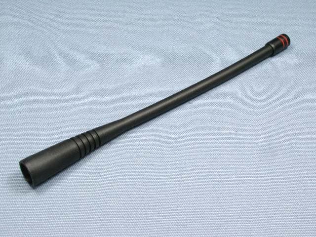
Click to zoom
Application Details
- Equipment Class
- TNF - Licensed Non-Broadcast Transmitter Held to Face
- Date of Grant
- Dec 01, 2014
- Application Purpose
- Original Equipment
- Date of Application
- Dec 01, 2014
- Equipment Note
- 2 WAY PORTABLE RADIO
- Frequency Range
- 403.00000000 - 406.00000000
- Company
- Vertex Standard USA, Inc.
- Country
- United States
Documents & Files
Document Text
Text extracted from the exhibit documents filed with the FCC. Open a document above to read the original.
Users Manual
To install the battery, hold the transceiver with your left hand, so your palm is over the speaker and your thumb is on the top of the belt clip. Insert the battery pack into the battery compartment on the back of the radio while tilt- ing the Belt Clip outward, then push the bottom side of the battery pack until the battery pack locks with the Battery Pack Latch. OperatiOnBefOre YOu Begin Battery Pack InstallatIon and removal PrelImInary stePs Install a charged battery pack onto the transceiver, as described previously. Screw the supplied antenna onto the Antenna jack. Never attempt to operate this transceiver without an antenna connected. If you have a Speaker/Microphone, we recommend that it not be connected until you are familiar with the basic operation of the VX-350 . oPeratIon QuIck start Turn the top panel’s VOL/PWR knob clockwise to turn on the radio on. Turn the top panel’s CH selector knob to choose the desired operating channel. Rotate the VOL/PWR knob to set the volume level. If no signal is present, press and hold in the Programmable key assigned to “SQL OFF” for more than one second; background noise will now be heard, and you may use this to set the VOL/ PWR knob for the desired audio level. Press and hold in the Programmable key as- signed to “SQL OFF” for more than one second (or press the key twice) to quiet the noise and resume normal (quiet) monitoring. To transmit, monitor the channel and make sure it is clear. To transmit, press and hold in the PTT switch. Speak into the microphone area of the front panel grille (lower right-hand corner) in a normal voice level. To return to the Receive mode, release the PTT switch. Do not transmit the radio without an antenna connected. Warning! fCC rf expOsure requirements This Radio has been tested and complies with the Federal Communications Commission (FCC) RF exposure limits for Occupational Use/Controlled ex- posure environment. In addition, it complies with the following Standards and Guidelines: FCC 96-326, Guidelines for Evaluating the Environmental Effects of Radio-Frequency Radiation. FCC OET Bulletin 65 Edition 97-01 (1997) Supplement C, Evaluating Compliance with FCC Guidelines for Human Exposure to Radio Frequen- cy Electromagnetic Fields. ANSI/IEEE C95.1-1992, IEEE Standard for Safety Levels with Respect to Human Exposure to Radio Frequency Electromagnetic Fields, 3kHz to 300 GHz. ANSI/IEEE C95.3-1992, IEEE Recommended Practice for the Measurement of Potentially Hazardous Electromagnetic Fields-RF and Microwave. WARNING: This radio generates RF electromagnetic energy during transmit mode. This radio is designed for and classified as Occupational Use Only, meaning it must be used only during the course of employment by individu- als aware of the hazards, and the ways to minimize such hazards. This radio is not intended for use by the General Population in an uncon- trolled environment. CAUTION: To ensure that your expose to RF electromagnetic energy is within the FCC allowable limits for occupational use, always adhere to the following guidelines: Please read this manual carefully to become familiar with the features of this transceiver. Do not transmit the radio without an antenna connected. This radio is NOT approved for use by the general population in an uncontrolled environment. This radio is restricted to occupational use, work related operations only where the radio operator must have the knowledge to control its RF exposure conditions. When transmitting, hold the radio in a vertical position with its mi- crophone 1 to 2 inches (2.5 to 5 cm) away from your mouth and keep the antenna at least 1 inch (2.5cm) away from your head and body. The radio must be used with a maximum operating duty cycle not ex- ceeding 50 %, in typical Push-to-Talk (PTT) configurations. DO NOT transmit for more than 50 % of total radio use time (50 % duty cycle). Transmitting more than 50 % of the time can cause FCC RF exposure compliance requirements to be exceeded. To keep the Body Worn configuration with the Vertex Standard CLIP- 18 belt-clip, reduce the maximum operating duty cycle still more. The radio is transmitting when the red LED on the top of the radio is illuminated. You can cause the radio to transmit by pressing the PTT button. When operate the radio with the Vertex Standard CLIP-18 belt-clip, make the transmission time as short as possible, to keep the Body Worn configuration. Always use the FNB-V96LIA or FNB-V130LI-UNI Lithium-Ion Bat- tery. Perform the battery charging where the ambient temperature range +10 °C to +40 °C. Charge out of this range could cause damage to the battery pack. Battery Pack shall not be exposed to excessive heat such as sunshine, fire or the like. Always use Vertex Standard authorized accessories. Vertex Standard shall not be liable for any damage or accidents such as fire, leakage or explosion of batteries, etc., caused by the malfunc- tion of non-Vertex Standard accessories. The information listed above provides the user with the information needed to make him or her aware of RF exposure, and what to do to assure that this radio operates with the FCC RF exposure limits of this radio. Electromagnetic Interference/Compatibility During transmissions, this radio generates RF energy that can possibly cause interference with other devices or systems. To avoid such interfer- ence, turn off the radio in areas where signs are posted to do so. Do not operate the transmitter in areas that are sensitive to electromag- netic radiation such as hospitals, health care facilities, aircraft, and blast- ing sites. FCC License Information This radio operates on communications frequencies which are subject to FCC (Federal Communications Commission) Rules and Regulations. FCC Rules require that all operators using Private Land Mobile radio frequencies obtain a radio license before operating their equipment. aCCessOries & OptiOns FNB-V96LIA 7.4 V , 2300 mAh Li-Ion Batt…
Text truncated - open the document above for the full version.
Attestation Statements
FCC ID: AXI10654620 VERTEX STANDARD USA, INC. Exhibit 13a 8000 West Sunrise Boulevard, Fort Lauderdale, Florida 33322 Date: November 20, 2014 Office of Engineering and Technology Laboratory Division Equipment Authorization Branch Federal Communications Commission Laboratory 7435 Oakland Mills Road Columbia, MD 21046 Subject: Application for Certification of Transmitter with FCC ID: AXI10654620 Dear Sir or Madam: Vertex Standard USA, Inc. (8000 West Sunrise Boulevard, Fort Lauderdale, Florida) herein submits application for certification of the subject transmitter. This transmitter is intended for use in a Mobile Radio environment and is capable of operating at the frequency range and power listed below: Model Frequency Rated Power FCC Rule Parts VX-351-G6-5 VX-354-G6-5 403-470 MHz 1-5 W 90 The subject transmitter complies with Section 90.203 of the Rules in that the operator cannot directly program transmit frequencies using the unit's normally accessible external controls. Enclosed is a complete Certification Application. Please contact me if you require any additional information. Sincerely, Kim Uong Regulatory Compliance Engineer Tel: (954) 723-5422 E-mail: [email protected]
Cover Letter(s)
FCC ID: AXI10654620 VERTEX STANDARD USA, INC. Exhibit 13b 8000 West Sunrise Boulevard, Fort Lauderdale, Florida 33322 CONFIDENTIALITY REQUESTED Date: November 20, 2014 Office of Engineering and Technology Laboratory Division Equipment Authorization Branch Federal Communications Commission Laboratory 7435 Oakland Mills Road Columbia, MD 21046 Subject: Confidentiality Request Regarding Application for Transmitter with FCC ID: AXI10654620 Dear Sir or Madam: Vertex Standard USA, Inc. (8000 West Sunrise Boulevard, Fort Lauderdale, Florida) is requesting for the following Exhibits be held as Permanently Confidential, and not be made routinely available for public inspection: Block diagram Schematics The information in these exhibits considers to be classified as trade secrets, pursuant to 47 CFR Sections 0.457(d), 0.459 and 552(b)(4) of the Freedom of Information Act. Please mark these Exhibits as “Confidential.” Please contact me if you require any additional information. Sincerely, Kim Uong Regulatory Compliance Engineer Tel: (954) 723-5422 E-mail: [email protected]
Cover Letter(s)
FCC ID: AXI10654620 VERTEX STANDARD USA, INC. Exhibit 13c 8000 West Sunrise Boulevard, Fort Lauderdale, Florida 33322 Date: November 20, 2014 Office of Engineering and Technology Laboratory Division Equipment Authorization Branch Federal Communications Commission Laboratory 7435 Oakland Mills Road Columbia, MD 21046 Subject: Extended Frequencies Justification for Certification of Transmitter with FCC ID: AXI10654620 Dear Sir or Madam: This transmitter was design to operate in the frequency range of 403-470 MHz. To aid equipment authorization in other countries that accept the United States FCC Grant for Certification, Vertex Standard USA Inc is requesting that the FCC list the above frequency/frequencies under FCC Rule Part 90 on the Grant. For the FCC’s Rule Part 90 applications, this radio is used in systems by Federal and Public Safety agencies including Police, Fire, and Emergency Medical Services, etc. as indicated in the table below. Equipment programming is the responsibility of Authorized Service Personnel. Also, the radio complies with 47 CFR Part 90.203(e), in that the operator cannot directly program the transmit frequencies using the normally accessible external controls. Per the FCC’s KDB634817 guidance, as an alternative to listing the exact frequencies, we acknowledge that it’s a violation of the FCC Rules if this device operates on unauthorized frequencies. Frequency Range (MHz) Part 90 Federal Emission Designator 403-406 x 11K0F3E 406.1-454 x 454-456* 456-470 x *Canada Please contact me if you require any additional information. Sincerely, Kim Uong Regulatory Compliance Engineer Tel: (954) 723-5422 E-mail: [email protected]
External Photos
FCC ID: AXI10654620 IC: 10239A-10654620 Vertex Standard LMR, Inc. Front view (VX-354) with antenna Front view (VX-351) with antenna FCC ID: AXI10654620 IC: 10239A-10654620 Vertex Standard LMR, Inc. Front view (VX-354) without antenna Front view (VX-351) without antenna FCC ID: AXI10654620 IC: 10239A-10654620 Vertex Standard LMR, Inc. Rear view with antenna Rear view without antenna FCC ID: AXI10654620 IC: 10239A-10654620 Vertex Standard LMR, Inc. Rear view without battery Left side FCC ID: AXI10654620 IC: 10239A-10654620 Vertex Standard LMR, Inc. Right side Top FCC ID: AXI10654620 IC: 10239A-10654620 Vertex Standard LMR, Inc. Bottom Battery Pack FNB-V130LI-UNI FCC ID: AXI10654620 IC: 10239A-10654620 Vertex Standard LMR, Inc. Battery Charger AC Adapter FCC ID: AXI10654620 IC: 10239A-10654620 Vertex Standard LMR, Inc. Speaker/Microphone MH-45B4B Speaker/Microphone MH-360S FCC ID: AXI10654620 IC: 10239A-10654620 Vertex Standard LMR, Inc. Speaker/Microphone MH-450S Earpiece Microphone MH-37A4B FCC ID: AXI10654620 IC: 10239A-10654620 Vertex Standard LMR, Inc. Antenna
ID Label/Location Info
VX-351-G6-5 / VX-354-G6-5VX-351-G6-5 / VX-354-G6-5 LABEL DRAWINGLABEL DRAWING Vertex Standard LMR, Inc.Vertex Standard LMR, Inc. ID / Part 15.19 and CAUTION drawings ID drawing Part 15.19 and CAUTION drawings Label location ! ! Device restricted to occupational use to satisfy FCC RF exposure compliance. See owner's manual for specific operating requirement CAUTION This device complies with part 15 of the FCC Rules. Operation is sublect to the condition that this device does not cause harmful interference. VX-354-G6-5 FCC ID: AXI10654620 788026126989 VERTEX STANDARD LMR,INC. ASSEMBLED IN CHINA 1D4I080531 SER. NO. 6.7-8.1V IC:10239A-10654620 CMIIT ID:2010FP4615 DESIGNED IN JAPAN VX-351-G6-5 FCC ID: AXI10654620 788026126989 VERTEX STANDARD LMR,INC. ASSEMBLED IN CHINA 1D4I080531 SER. NO. 6.7-8.1V IC:10239A-10654620 CMIIT ID:2010FP4614 DESIGNED IN JAPAN 2014. 11. 142014. 11. 14 FCC ID: AXI10654620 IC: 10239A-10654620
Internal Photos
FCC ID: AXI10654620 IC: 10239A-10654620 Vertex Standard LMR, Inc. Inside view Side-A of MAIN-5-UNIT with LCD FCC ID: AXI10654620 IC: 10239A-10654620 Vertex Standard LMR, Inc. Side-A of MAIN-5-UNIT without LCD Side-B of MAIN-5-UNIT with shield case FCC ID: AXI10654620 IC: 10239A-10654620 Vertex Standard LMR, Inc. Side-B of MAIN-5-UNIT without shield case Top of LCD FCC ID: AXI10654620 IC: 10239A-10654620 Vertex Standard LMR, Inc. Bottom of LCD Inside of front panel (for VX-354) FCC ID: AXI10654620 IC: 10239A-10654620 Vertex Standard LMR, Inc. Inside of front panel (for VX-351) Inside of chassis FCC ID: AXI10654620 IC: 10239A-10654620 Vertex Standard LMR, Inc. PWB of Battery Charger
Operational Description
FCC ID: AXI10654620 IC: 10239A-10654620 Circuit Description 1/3 VX-350 Series Circuit Description 1. Circuit Configuration by Frequency The receiver is a Double-conversion Super-heterodyne with a first intermediate frequency (IF) of 50.85 MHz and a second IF of 450 kHz. Incoming signal from the antenna is mixed with the local signal from the VCO/PLL to produce the first IF of 50.85 MHz. This is then mixed with the 50.4 MHz second local oscillator output to produce the 450kHz second IF. This is detected to give the demodulated signal. The transmit signal frequency is generated by the PLL VCO, and modulated by the signal from the microphone. It is then amplified and sent to the antenna. 2. Receiver System 2-1. Front-end RF amplifier Incoming RF signal from the antenna is delivered to the RF Unit and passes through Low-pass filer, antenna switching diode D5003 (JDP2S12CR), high pass filter and removed undesired frequencies by varactor diodes D5007 and 5009 (both 1SV331)(tuned band-pass filer). The passed signal is amplified in Q5021 (MSG33001) and moreover cuts an image frequency with the tuned band pass filter D5016 and 5018 (both 1SV331) and comes into the 1st mixer. 2-2. First Mixer The 1st mixer consists of the Q5036 (3SK293). Buffered output from the VCO is amplified by Q5031 (2SC5005) to provide a pure first local signal between 352.15 and 419.15 MHz for injection to the first mixer. The IF signal then passes through monolithic crystal filters XF5001 (±5.5 kHz BW) to strip away all but the desired signal. 2-3. IF Amplifier The first IF signal is amplified by Q5048 (2SC5226). The amplified first IF signal is applied to FM IF subsystem IC Q5053 (NJM2591) which contains the second mixer, second local oscillator, limiter amplifier, noise amplifier, and S-meter amplifier. The signal from reference oscillator X5002 becomes 3 times of frequencies in Q1053, it is mixed with the IF signal and becomes 450 kHz. The second IF then passes through the ceramic filter CF5001 (LTM450EW: wide channels), CF5002 (LTM450GW: narrow channels) to strip away unwanted mixer products, and is applied to the limiter amplifier in Q5053, which removes amplitude variations in the 450kHz IF, before detection of the speech by the ceramic discriminator CD5001 (JTBM450CX24). 2-4. Audio amplifier Detected signal from Q1053 is inputted to mute switch Q5001- 3 (SN74LV4066APWR) and option switch Q5001-2. The signal which appeared from Q5001-2 is in band pass filter Q5066 (NJM12902V). In the case an optional unit is installed, the Q5001-2 is made “OFF” and the AF signal from Q5001-3 goes the optional unit. In the case an optional unit is not installed, Q5001-2 is made “ON” and the signal goes through Q5001-2. The signal which passed Q5066 goes to AF volume (VR5001). And then the signal goes to audio amplifier Q5007(NJM2070M). The output signal from Q5007 is in audio speaker. 2-5. Squelch Circuit There are 16 levels of squelch setting from “0” to “15”. The level “0” means open the squelch. The level 1 means the threshold setting level and level “14” means tight squelch. From “2” to “13” is established in the middle of threshold and tight. The bigger figure is nearer the tight setting. The level “15” becomes setting of carrier squelch. Vertex Standard LMR, Inc. FCC ID: AXI10654620 IC: 10239A-10654620 Circuit Description 2/3 2-5-1. Noise Squelch Noise squelch circuit is composed of the band path filter of Q5053, noise amplifier Q5058 (2SC4617), and noise detector D5042 and D5043 (both DA221). When a carrier isn’t received, the noise ingredient which goes out of the demodulator Q5053 is amplified in Q5058 through the band path filter Q5053, is detected to DC voltage with D5042 and D5043 and is inputted to 48 pin (the A/D port) of the Q5044 (CPU: LC87F5864B). When a carrier is received, the DC voltage becomes low because the noise is compressed. When the detected voltage to CPU is high, the CPU stops AF output with Q5001-1 “OFF” by making the 39 pin (CPU) “L” level. When the detection voltage is low, the CPU makes Q5001-1 “ON” with making 39 pin “H” and the AF signal is output. 2-5-2. Carrier Squelch The CPU (47 pin: A/D port) detect RSSI voltage output from Q5053 12 pin, and controls AF output. The RSSI output voltage changes according to the signal strength of carrier. The stronger signal makes the RSSI voltage to be higher voltage. The process of the AF signal control is same as Noise Squelch. The shipping data is adjusted 3dB higher than squelch tight sensitivity. 3. Transmitter System 3-1. Mic Amplifier The AF signal from internal microphone MC5001 or external microphone J5002 is amplified with microphone amplifier Q5069-2 (NJM12904), after passes microphone gain volume Q5017-CH1 (M62364FP). AF signal is passes a pre-emphasis circuit. Q5001-1 (SN74LV4066APW) becomes “OFF” when an option unit is attached and the AF signal from Q5068 goes via the option unit. When an option unit isn't attached, Q5001-1 becomes “ON”, the signal passes Q5001-1 and is input to the limiter amplifier Q5068-2 (NJM12902V). The signal passed splatter filter of Q5068 and adder amplifier Q5065 is adjusted by maximum deviation adjustment volume Q5017- CH4 (M62364FP). The AF signal ingredient is amplified Q5065 (NJM12902V). After that, it is made FM modulation to transmit carrier by the modulator D5023 (HVC383) of VCO. 3-2. Drive and Final amplifier The modulated signal from the VCO Q5049 (2SC4227) is buffered by Q5042 (2SC5005) and amplified by Q5031 (2SC5005). Then the signal is buffered by Q5026 (2SC5998) for the final amplifier driver Q5020 (RD01MUS1). The lowlevel transmit signal is then applied to Q5013 (RD09MUP2) for final amplification up to 5watts output power. The transmit signal then passes through the antenna switch D5002 (HVU131) and is low pass filtered to suppress away harmonic spurious radiation before delivery to the antenna. 3-3. Automatic Transmit Power Control The current detector Q5064-1 (NJM12902V) detects the current of Q5013 and Q5…
Text truncated - open the document above for the full version.
Parts List/Tune Up Info
1 FCC ID: AXI10654620/IC: 10239A-10654620 VX-351/354-G6-5Semi-Conductor Parts List Address Parts Code Device NameDescription MAIN-5-UNIT D 5001 G2070634 Diode1SS400 TE61 D 5002 G2070462 DiodeHVU131 TRF-E D 5003 G2071446 DiodeHVU131 TRF-E D 5004 G2070118 DiodeHSU277TRF D 5005 G2070178 DiodeDA221 TL D 5006 G2070178 DiodeDA221 TL D 5007 G2071044 Diode1SV331(TPH3.F) D 5008 G2070634 Diode1SS400 TE61 D 5009 G2071044 Diode1SV331(TPH3.F) D 5010 G2070634 Diode1SS400 TE61 D 5012 G2070634 Diode1SS400 TE61 D 5013 G2071004 Zener DiodeEDZ TE-61 3.9B D 5014 G2070634 Diode1SS400 TE61 D 5015 G2070634 Diode1SS400 TE61 D 5016 G2071044 Diode1SV331(TPH3.F) D 5017 G2071172 LEDLTST-S326KGJRKT D 5018 G2071044 Diode1SV331(TPH3.F) D 5019 G2070174 DiodeDAN222 TL D 5020 G2070634 Diode1SS400 TE61 D 5022 G2070908 Zener DiodeUDZS TE-17 5.1B D 5023 G2070922 DiodeHVC383B TRF-E D 5024 G2070178 DiodeDA221 TL D 5025 G2070178 DiodeDA221 TL D 5026 G2071162 DiodeHVC374B TRF-E D 5027 G2071162 DiodeHVC374B TRF-E D 5028 G2070634 Diode1SS400 TE61 D 5029 G2070934 Diode1SS400G T2R D 5030 G2070934 Diode1SS400G T2R D 5031 G2071006 Diode1SV323(TPH3.F) D 5032 G2070934 Diode1SS400G T2R D 5033 G2071006 Diode1SV323(TPH3.F) D 5034 G2070934 Diode1SS400G T2R D 5035 G2070848 Diode1SV325(TPH3.F) D 5036 G2070848 Diode1SV325(TPH3.F) D 5037 G2071358 LEDHSML-C191 D 5038 G2070634 Diode1SS400 TE61 D 5039 G2070174 DiodeDAN222 TL D 5040 G2070174 DiodeDAN222 TL D 5041 G2070634 Diode1SS400 TE61 D 5042 G2070178 DiodeDA221 TL D 5043 G2070178 DiodeDA221 TL D 5044 G2070634 Diode1SS400 TE61 D 5046 G2070716 DiodeBAS316 D 5047 G2071044 Diode1SV331(TPH3.F) DS5001 G6090194A LCDDTE105793CWZ Q 5001 G1093871 ICSN74LV4066APWR Q 5002 G3117748R Transistor2SA1774 TL R Q 5003 G3070225 TransistorDTC114TE TL Q 5004 G3070143 TransistorXP1501-(TX) Q 5005 G3211327R Transistor2SB1132 T100 R Q 5006 G1094097 ICTAR5S50U(TE85L.F) Q 5007 G1094509 ICNJM2070M-TE1 Q 5008 G3070075 TransistorDTC144EE TL VX-354 Only VX-354 Only VX-354 Only Vertex Standard LMR, Inc. 2 FCC ID: AXI10654620/IC: 10239A-10654620 VX-351/354-G6-5Semi-Conductor Parts List Address Parts Code Device NameDescription Q 5009 G3070223 TransistorCPH6102-TL Q 5010 G3070343 TransistorUMD5N TR Q 5012 G3346178R Transistor2SC4617 TL R Q 5013 G3070367 MOSFETRD09MUP2(TAPE) Q 5014 G3070225 TransistorDTC114TE TL Q 5015 G3070075 TransistorDTC144EE TL Q 5016 G3070075 TransistorDTC144EE TL Q 5017 G1093033 ICM62364FP 600D Q 5018 G3070075 TransistorDTC144EE TL Q 5019 G3070075 TransistorDTC144EE TL Q 5020 G3070321 MOSFETRD01MUS1-T113 Q 5021 G3070348 TransistorMSG330010L Q 5022 G3070075 TransistorDTC144EE TL Q 5023 G3070225 TransistorDTC114TE TL Q 5024 G3346178R Transistor2SC4617 TL R Q 5025 G3070225 TransistorDTC114TE TL Q 5026 G3359988 Transistor2SC5998YC-TL-E Q 5027 G3070225 TransistorDTC114TE TL Q 5028 G3340818 Transistor2SC4081 T106 Q 5029 G1093606 ICS-80835CNMC-B8U-T2-G Q 5030 G1094096 ICTAR5S35U(TE85L.F) Q 5031 G3350058 Transistor2SC5005-T1 Q 5032 G3211327R Transistor2SB1132 T100 R Q 5033 G3070225 TransistorDTC114TE TL Q 5034 G3070143 TransistorXP1501-(TX) Q 5035 G3070225 TransistorDTC114TE TL Q 5036 G4802938 FET3SK293(TE85L,F) Q 5038 G3070074 TransistorDTA144EE TL Q 5039 G3070225 TransistorDTC114TE TL Q 5040 G1093874 ICBR93L66RFVM-WTR Q 5041 G3070225 TransistorDTC114TE TL Q 5042 G3350058 Transistor2SC5005-T1 Q 5043 G3070225 TransistorDTC114TE TL Q 5044 G1094436 ICLC87F5864C-F58F1-E Q 5045 G3070074 TransistorDTA144EE TL Q 5046 G3805088B FET2SK508-T1B-A K52 Q 5047 G3070225 TransistorDTC114TE TL Q 5048 G3352268Z Transistor2SC5226-4/5-TL Q 5049 G3342278B Transistor2SC4227-T1 R32 Q 5050 G3346178R Transistor2SC4617 TL R Q 5051 G3070075 TransistorDTC144EE TL Q 5052 G3350058 Transistor2SC5005-T1 Q 5053 G1094024 ICNJM2591V-TE1 Q 5054 G3340818 Transistor2SC4081 T106 Q 5055 G3070075 TransistorDTC144EE TL Q 5056 G3808807G FET2SK880GR(TE85R.F) Q 5057 G1093288 ICLC75834W Q 5058 G3346178R Transistor2SC4617 TL R Q 5059 G1094714 ICAK1542 Q 5061 G3070075 TransistorDTC144EE TL Q 5062 G3070075 TransistorDTC144EE TL Q 5064 G1093592 ICNJM12902V-TE1 Q 5065 G1093592 ICNJM12902V-TE1 Q 5066 G1093592 ICNJM12902V-TE1 VX-354 Only VX-354 Only VX-354 Only Vertex Standard LMR, Inc. 3 FCC ID: AXI10654620/IC: 10239A-10654620 VX-351/354-G6-5Semi-Conductor Parts List Address Parts Code Device NameDescription Q 5067 G1093592 ICNJM12902V-TE1 Q 5068 G1093592 ICNJM12902V-TE1 Q 5069 G1093337 ICNJM12904R-TE1 Q 5070 G3070074 TransistorDTA144EE TL Q 5071 G1093337 ICNJM12904R-TE1 Vertex Standard LMR, Inc.
Parts List/Tune Up Info
FCC ID: AXI10654620 IC: 10239A-10654620 Alignment 1/4 VX-350 Series Alignment Introduction The VX-350 series are carefully aligned at the factory for the specified performance across the frequency range specified for each version. Realignment should therefore not be necessary except in the event of a component failure, or altering version type. All component replacement and service should be performed only by an authorized Vertex Standard representative, or the warranty policy may be voided. The following procedures cover the sometimes critical and tedious adjustments that are not normally required once the transceiver has left the factory. However, if damage occurs and some parts subsequently are placed, realignment may be required. If a sudden problem occurs during normal operation, it is likely due to component failure; realignment should not be done until after the faulty component has been replaced. We recommend that servicing be performed only by authorized Vertex Standard service technicians who are experienced with the circuitry and fully equipped for repair and alignment. Therefore, if a fault is suspected, contact the dealer from whom the transceiver was purchased for instructions regarding repair. Authorized Vertex Standard service technicians realign all circuits and make complete performance checks to ensure compliance with factory specifications after replacing any faulty components. Those who do undertake any of the following alignments are cautioned to proceed at their own risk. Problems caused by unauthorized attempts at realignment are not covered by the warranty policy. Also, Vertex Standard reserves the right to change circuits and alignment procedures in the interest of improved performance, without notifying owners. Under no circumstances should any alignment be attempted unless the normal function and operation of the transceiver are clearly understood, the cause of the malfunction has been clearly pinpointed and any faulty components replaced, and realignment determined to be absolutely necessary. The following test equipment (and thorough familiarity with its correct use) is necessary for complete realignment. Correction of problems caused by misalignment resulting from use of improper test equipment is not covered under the warranty policy. While most steps do not require all of the equipment listed, the interactions of some adjustments may require that more complex adjustments be performed afterwards. Do not attempt to perform only a single step unless it is clearly isolated electrically from all other steps. Have all test equipment ready before beginning, and follow all of the steps in a section in the order presented. Vertex Standard LMR, Inc. FCC ID: AXI10654620 IC: 10239A-10654620 Alignment 2/4 Required Test Equipment RF Signal Generator with calibrated output level at 600MHz for UHF Deviation Meter (linear detector) In-line Wattmeter with 5% accuracy at 600MHz for UHF 50-Ω RF Dummy Load with power rating 10W at 600MHz for UHF 4Ω/1W AF Dummy Load Regulated DC Power Supply (standard 7.5V DC, 3A) Frequency Counter with 0.2ppm accuracy at 600MHz for UHF Audio Signal Generator (available to output 30Hz to 5kHz) AC Voltmeter DC Voltmeter Computer with Microsoft Windows98SE or later operating system Vertex Standard CE86 Alignment Programming software and CT-42 Connection Cable or FIF-12A USB Programming Interface and CT-106 PC Programming Cable. Alignment Preparation & Precautions A 50-Ω RF Dummy Load and in-line wattmeter must be connected to the main antenna jack in all procedures that call for transmission, except where specified otherwise. Correct alignment is not possible with an antenna. After completing one step, read the following step to determine whether the same test equipment will be required. If not, remove the test equipment (except dummy load and wattmeter, in connected) before proceeding. Correct alignment requires that the ambient temperature be the same as that of the transceiver and test equipment, and that this temperature be held constant between 20°C and 30°C (68°F ∼ 86 °F). When the transceiver is brought into the shop from hot or cold air, it should be allowed time to come to room temperature before alignment. Whenever possible, alignments should be made with oscillator shields and circuit boards firmly affixed in place. Also, the test equipment must be thoroughly warmed up before beginning. Note: Signal levels in dB referred to in the alignment procedure are based on 0dB μ EMF = 1μV. Vertex Standard LMR, Inc. FCC ID: AXI10654620 IC: 10239A-10654620 Alignment 3/4 Test Setup Setup the test equipment as shown for transceiver alignment, apply 7.5V DC power to the transceiver. Refer to the drawings above for Alignment Points. The transceiver must be programmed for use in the intended system before alignment is attempted. The RF parameters are loaded from the file during the alignment process. In order to facilitate alignment over the complete switching range of the equipment it is recommended that the channel data in the transceiver is preset as the chart below. Channels Frequency (Simplex) VHF UHF-A UHF-D Band-LOW 134.100MHz 400.100MHz 450.100MHz Band-MID 154.100MHz 435.100MHz 480.100MHz Band-HIGH 173.900MHz 469.900MHz 511.900MHz The alignment mode is accessed by “Alignment mode” command from the computer whilst switching on. And the alignment tool operates it automatically. During the alignment mode, normal operation is suspended. Use the alignment tool program running on PC. The alignment tool outline Installation the tool Install the CE86 Alignment Program to your PC. The re-alignment for VX-350 series may use the “Alignment” menu of CE86. Action of the switches When the transceiver is in alignment mode, the action of [PTT], [KEY] is ignored. All of the action is remote controlled by PC. Vertex Standard LMR, Inc. FCC ID: AXI10654620 IC: 10239A-10654620 Alignment 4/4 Basic sequence The data displayed in screen of thi…
Text truncated - open the document above for the full version.
RF Exposure Info
802 N. Twin Oaks Valley Road, Suite 105 • San Marcos, CA 92069 • U.S.A. TEL (760) 471-2100 • FAX (760) 471-2121 http://www.rfexposurelab.com CERTIFICATE OF COMPLIANCE SAR EVALUATION Vertex Standard USA Inc. Dates of Test: November 10-12, 2014 8000 West Sunrise Blvd. Test Report Number: SAR.20141103 Ft. Lauderdale, FL 33322 Revision B This wireless mobile and/or portable device has been shown to be compliant for localized specific absorption rate (SAR) for uncontrolled environment/general exposure limits specified in ANSI/IEEE Std. C95.1-1992 and had been tested in accordance with the measurement procedures specified in IEEE 1528-2003, IEC62209 and RSS-102 (See test report). I attest to the accuracy of the data. All measurements were performed by myself or were made under my supervision and are correct to the be…
Text truncated - open the document above for the full version.
Contact Information
Applicant
Arine Lee(Certification Manager)
Technical Contact
Timco Engineering, Inc.Cory Leverett
[email protected]888-472-2424
849 NW State Road 45 · Newberry, Florida · United States
Non-Technical Contact
Timco Engineering, Inc.Sharon Hoffman
[email protected]888-472-2424
Test Firm
Timco Engineering, Inc.Bruno Clavier
Technical Specifications
| # | Rule Parts | Frequency Range | Power Output | Emission | Tolerance |
|---|---|---|---|---|---|
| 4 | 9 | 403 MHz - 406 MHz | 5 W | 11K0F3E | 2.5 ppm |
Other Applications from Vertex Standard USA, Inc.
AXI11284620
Jun 30, 20152-WAY PORTABLE RADIO
Equipment Class
TNF - Licensed Non-Broadcast Transmitter Held to Face
AXI11274620
Jun 30, 20152-WAY PORTABLE RADIO
Equipment Class
TNF - Licensed Non-Broadcast Transmitter Held to Face
AXI11273020
Dec 28, 2014VHF HANDHELD LAND MOBILE RADIO
Equipment Class
TNF - Licensed Non-Broadcast Transmitter Held to Face
AXI11283020
Dec 28, 2014VHF HANDHELD LAND MOBILE RADIO
Equipment Class
TNF - Licensed Non-Broadcast Transmitter Held to Face
AXI11143030
Dec 07, 2014VHF MOBILE TWO-WAY RADIO
Equipment Class
TNB - Licensed Non-Broadcast Station Transmitter