BZ5MXI1002UDigital Television Translator
Larcan Inc
Click to zoom
Application Details
- Equipment Class
- TBC - Licensed Broadcast Station Transmitter
- Date of Grant
- Jul 11, 2012
- Application Purpose
- Original Equipment
- Date of Application
- May 28, 2012
- Equipment Note
- Digital Television Translator
- Frequency Range
- 614.00000000 - 806.00000000
- Company
- Larcan Inc
- Country
- Canada
Documents & Files
Document Text
Text extracted from the exhibit documents filed with the FCC. Open a document above to read the original.
Users Manual
MXi501U/1002U AMPLIFIER CHASSIS CONTENTS 1 MXi501U/1002U AMPLIFIER .........................................................................................................................................1 FIGURES FIGURE 1 MXI501U/1002U AMPLIFIER WIRING SCHEMATIC......................................................................................................2 PUB11-013 Rev 1 July 2011 11-013-i MXi501U/1002U Amplifier Chassis MXi501U/1002U AMPLIFIER CHASSIS 1 MXi501U/1002U AMPLIFIER The Amplifier Chassis Assemblies 41D2270G1&G2 consists of a standard 19" rack mountable 5.25" (3RU) enclosure containing the amplifier heatsink assembly, a fan array assembly consisting of four DC cooling fans, a controller board with built-in RF detectors and a rear panel assembly with connectors for interfacing to external equipment. The MXi501 chassis (G1) has a front panel consisting of ON/OFF, RESET switches and an LCD/Touchpad. The MXi1002 does not have these on the front panel as they are located in the power supply chassis The rear of the AMPLIFIER has the following connectors: • RS232 SERIAL nine-pin connector • REMOTE CONTROL 15-pin D-shell connector • RF IN SMA connector • INTERLOCK terminal board • RF TP SMA connector – RF sample • RF OUT N connector • Control/Auxiliary power supply connector. • 50V power supply connector. The amplifier is a broadband amplifier, thus it is operational to cover the entire UHF television spectrum ranging in frequencies from 470MHz to 860MHz. Main DC power to the amplifier assembly comes from the high efficiency switching power supply (separate chassis). There is a second auxiliary +12V power supply which is used for powering the controller and the cooling fans. The heatsink cooling fans are the +12VDC, 4-inch muffin model. They are energized when the controller turns on the main power supply to power amplifier. The voltage is supplied to the amplifier from the 12V six-pin connector on the rear panel and it is connected to the controller PC board connector, J8. As built, the cooling fans push air from the front panel through the heatsink. This assembly is located underneath the MXi Controller board. A thermal switch is mounted on the heatsink. If this temperature increases beyond the trip point of the thermal switch of 76°C, its contact opens and breaks the interlocking circuit of the MXi amplifier. The interlock circuit ultimately controls the power supply to the power amplifier and therefore shuts down and remains OFF until the heatsink cools down. A directional coupler is mounted at the rear of the heatsink and provides forward and reflected RF signals to the controller. These RF samples are detected and processed on the MXi controller to provide DC outputs corresponding to these signals. They are then used for AGC, VSWR supervision. The chassis is wired according to the functional diagram 41D2238 as shown in Figure 1 PUB11-013 Rev 1 July 2011 11-013-1 MXi501U/1002U Amplifier Chassis MXi501U/1 00 2U AMP L IFIER CHASSIS Figure 1 M X i 5 01U/1002U Amplifier Wir i ng Sc hem a tic PUB11- 013 R e v 1 Jul y 201 1 11-0 13-2 MXi 5 0 1 U/10 02 U Amplifier C h assis
Users Manual
MXi501/1002U POWER AMPLIFIER HEATSINK ASSEMBLY CONTENTS 1 POWER AMPLIFIER HEATSINK ASSEMBLY..........................................................................................................1 2 FRONT END MODULE ASSEMBLY 21B1473G7........................................................................................................2 3 DRIVER MODULE 21B2708G3......................................................................................................................................3 4 PA PALLET ASSEMBLY 21B2729G1............................................................................................................................4 5 FIVE-WAY SPLITTER/FIVE-WAY COMBINER .......................................................................................................5 6 DIRECTIONAL COUPLER 21B2746G1........................................................................................................................6 7 BENCH TEST PROCEDURES........................................................................................................................................7 7.1 FRONT-END MODULE, 21B1473G7, BENCH TEST PROCEDURE....................................................................................7 7.2 DRIVER PALLET, 21B2708G3, BENCH TEST PROCEDURE.............................................................................................7 7.3 PA PALLET 21B2729G1 BENCH TEST PROCEDURE......................................................................................................7 FIGURES FIGURE 1 MXI SUB-ASSEMBLIES.................................................................................................................................................1 FIGURE 2 21B1473 MXI FRONT END UHF DTV DRIVER ASSEMBLY..........................................................................................8 FIGURE 3 11A1354 MXI FRONT END UHF DTV DRIVER SCHEMATIC.........................................................................................9 FIGURE 4 21B2708S DRIVER PALLET ASSEMBLY......................................................................................................................10 FIGURE 5 21B2708S DRIVER PALLET SCHEMATIC.....................................................................................................................11 FIGURE 6 21B2729A1 PALLET CIRCUIT ASSEMBLY...................................................................................................................12 FIGURE 7 21B2729S1 PALLET CIRCUIT SCHEMATIC..................................................................................................................13 FIGURE 8 21B2444A1 5 WAY SPLITTER ASSEMBLY..................................................................................................................14 FIGURE 9 21B2444S1 5 WAY SPLITTER SCHEMATIC..................................................................................................................15 FIGURE 10 21B2445A1 5 WAY COMBINER ASSEMBLY..............................................................................................................16 FIGURE 11 21B2445S1 5 WAY COMBINER SCHEMATIC.............................................................................................................17 FIGURE 12 21B2446S1 DIRECTIONAL COUPLER ASSEMBLY......................................................................................................18 FIGURE 13 21B2446S1 DIRECTIONAL COUPLER SCHEMATIC.....................................................................................................19 PUB11-014 Rev 1 July 2011 11-014-i MXi501/1002U Power Amplifier Heatsink Assembly MXi501/1002U POWER AMPLIFIER HEATSINK ASSEMBLY 1 POWER AMPLIFIER HEATSINK ASSEMBLY The MXi Power Amplifier Heatsink Assembly 41D2272G1 consists of a fan-cooled heatsink and ten printed circuit board sub-assemblies. The first module is a pre-amplifier, known as the Front-End Module. This first stage is operated in Class A mode. Next is the Driver pallet, which is biased so as to pre-correct for the non-linearity in the final amplifier stage. The next stage is a five-way splitter that splits the RF power so it can be fed to the PA pallets. The final amplifier stage is the PA pallets. After the pallets is the five-way combiner which combines the output power from the PA pallets. The last sub-assembly on the heatsink is the directional coupler which detects the forward and reflected power and provides samples to the control board and a RF test point on the rear panel. Also mounted on the heatsink is a thermal switch, which protects the amplifiers from over-temperature conditions such as the absent of cooling or amplifier over dissipation. This heatsink assembly is mounted in the Amplifier Chassis Assembly 41D2270G1 or G2. Descriptions of each stage are detailed in the following pages. Figure 1 MXi Sub-Assemblies The above picture illustrates the arrangement of the sub-assemblies on the amplifier heatsink assembly. From right to left are the Front-End and Driver modules. Centered and towards the back are the Splitter, PA modules and the Combiner. At the very back is the Directional Coupler. Strategically installed on the heatsink, is a thermal switch which protects the amplifier from over temperature conditions. Cooling for the heatsink is provided by a fan array assembly consisting of four 4-inch axial flow +12VDC muffin fans. This array is situated near the front section of the MXi housing underneath the MXi Amplifier Controller PC board. The fans blow air into the finned portion of the heatsink, which exhausts through the rear. PUB11-014 Rev 1 July 2011 11-014-1 MXi501/1002U Power Amplifier Heatsink Assembly MXi501/1002U POWER AMPLIFIER HEATSINK ASSEMBLY 2 FRONT END MODULE ASSEMBLY 21B1473G7 Drawing Reference: Figure 2 and Figure 3 The front end module performs several distinctive functions. Firstly, it serves as a pre-amplifier, which boosts the signal from the up-converter by …
Text truncated - open the document above for the full version.
Users Manual
AMPLIFIER CONTROLLER BOARD REV.3 CONTENTS 1 INTRODUCTION.....................................................................................................................................................1 2 GENERAL OPERATIONS ......................................................................................................................................2 2.1 CONNECTOR AND SIGNAL DEFINITIONS........................................................................................................................2 2.1.1 J1 BDM (Background Debug Mode) Connection................................................................................................2 2.1.2 J2 Remote RS232 Connection..............................................................................................................................2 2.1.3 J3 Front Panel LCD and Touchpad.....................................................................................................................2 2.1.4 J4 +50 Volt DC Power Supply.............................................................................................................................2 2.1.5 J5 +50 Volt DC Power Supply Sensing (External)..............................................................................................2 2.1.6 J6 Remote Interface.............................................................................................................................................2 2.1.7 J7 Transmitter Switch Interface...........................................................................................................................3 2.1.8 J8 Fan Interface...................................................................................................................................................3 2.1.9 J9 External Controls............................................................................................................................................3 2.1.10 J10 AGC Control.................................................................................................................................................3 2.1.11 J11 Aural Detector (Optional).............................................................................................................................3 2.1.12 J12 Forward RF Sample......................................................................................................................................3 2.1.13 J13 Reflected RF Sample.....................................................................................................................................3 2.1.14 J14 Front Panel LCD Power...............................................................................................................................3 2.2 JUMPER OPTIONS..........................................................................................................................................................3 2.2.1 BDM Slide Switch S2...........................................................................................................................................3 2.3 RF DETECTOR OPERATION...........................................................................................................................................6 2.4 AGC, VSWR AND CUTBACK OPERATION....................................................................................................................7 2.5 INTERLOCKS.................................................................................................................................................................8 2.5.1 Hard Interlocks ....................................................................................................................................................8 2.5.2 Soft Interlocks......................................................................................................................................................9 2.6 EXTERNAL SIGNALS AND REMOTE CONTROL...............................................................................................................9 2.6.1 External #1 Interlock...........................................................................................................................................9 2.6.2 Remote Interface (Individual)............................................................................................................................10 2.6.3 Serial Interface ..................................................................................................................................................10 2.6.4 Transmitter Switching Interface.........................................................................................................................10 2.6.5 External DC Power Supply................................................................................................................................10 3 SETUP PROCEDURES ..........................................................................................................................................11 3.1 RF DETECTOR............................................................................................................................................................11 3.1.1 Test Equipment Required...................................................................................................................................11 3.1.2 Jumper Installation............................................................................................................................................11 3.1.3 Verify OpAmp Offsets........................................................................................................................................12 3.1.4 Verify Output Power Level.................................................................................................................................12 3.2 CUTBACK PROTECTION..............................................…
Text truncated - open the document above for the full version.
Users Manual
MXI1002 OPERATIONS AND MAINTENANCE CONTENTS 1 THE MXi1002 TRANSMITTER......................................................................................................................................2 2 MXi1002U AMPLIFIER HEATSINK ASSEMBLY......................................................................................................3 3 MXi AMPLIFIER CONTROLLER.................................................................................................................................4 4 AMPLIFIER INSTALLATION AND STARTUP..........................................................................................................5 4.1 BEFORE APPLYING AC TO THE UNIT............................................................................................................................5 4.2 APPLYING AC TO THE UNIT..........................................................................................................................................5 4.3 BEFORE TURNING THE AMPLIFIER ON.........................................................................................................................6 4.4 AMPLIFIER ON SEQUENCE............................................................................................................................................6 4.4.1 Turning ON the MXi Transmitter.........................................................................................................................7 4.4.2 TYPICAL DATA read on the LCD.......................................................................................................................8 5 TEST AND TROUBLESHOOTING...............................................................................................................................9 5.1 BASIC TROUBLESHOOTING TECHNIQUES......................................................................................................................9 5.1.1 No RF Output.......................................................................................................................................................9 5.1.2 Output Reduced to 25%.......................................................................................................................................9 6 MAINTENANCE.............................................................................................................................................................10 6.1 DAILY.........................................................................................................................................................................10 6.2 MONTHLY...................................................................................................................................................................10 6.3 SEMI-ANNUALLY AND ANNUALLY.............................................................................................................................10 6.4 TRANSMITTER COOLING SYSTEM...............................................................................................................................10 7 SERVICE..........................................................................................................................................................................11 7.1 REMOVING THE FAN ARRAY.......................................................................................................................................11 7.2 REPLACING THE ENTIRE FAN ARRAY.........................................................................................................................12 8 TEST EQUIPMENT SETUP..........................................................................................................................................13 9 SPECIFICATIONS.........................................................................................................................................................14 9.1 ELECTRICAL...............................................................................................................................................................14 9.2 ENVIRONMENTAL.......................................................................................................................................................14 9.3 COOLING....................................................................................................................................................................14 9.4 DIMENSIONS...............................................................................................................................................................14 9.5 SHIPPING WEIGHT................................................................................................ERROR! BOOKMARK NOT DEFINED. FIGURES FIGURE 1 MXI1002 POWER SUPPLY (TOP), AND AMPLIFIERS.......................................................................................................2 FIGURE 2 MXI CONTROLLER........................................................................................................................................................4 FIGURE 3 REAR PANEL SHOWING INTERLOCK CONNECTOR.........................................................................................................5 FIGURE 4 MAIN MENU..................................................................................................................................................................6 FIGURE 5 INTERLOCKS STATUS....................................................................................................................................................6 FIGURE 6 TRANSMITTER ON........................................................................................................................................................7 FIGURE 9 BOTTOM VIEW OF MXI...............................................................................................................................................11 FIGU…
Text truncated - open the document above for the full version.
Users Manual
MXi1002U 2-WAY COMBINER CONTENTS 1 2-WAY COMBINER.........................................................................................................................................................1 FIGURES FIGURE 1 21B2741A1 MXI1002 2-WAY COMBINER ASSEMBLY SHEET 1 ...................................................................................2 FIGURE 2 21B2741A2 MXI1002 2-WAY COMBINER ASSEMBLY SHEET 2 ...................................................................................3 PUB11-019 Rev 0 July 8, 2011 11-019-i MXi1002U 2-Way Combiner MXi1002U 2-WAY COMBINER 1 2-WAY COMBINER The combiner module consists of a single 3dB quadrature hybrid coupler that combines the power at the two input ports. If there is a level difference between INPUT 1 and INPUT 2, then a portion of the difference is directed to the REJECT port. A air cooled 50 ohm termination connected to the REJECT port absorbs this difference power. If either of the inputs to the combiner module is shut down, then a maximum of 250W of reject power will be absorbed by the load on the REJECT port. The other half of the input power is directed to the output connector. The phase of the signals arriving at each input port 90 degrees out of phase as controlled by the 2 way splitter assembly located in the main controller inside the power supply chassis PUB07-010 Rev 0 January 9, 2007 07-010-1 MXi802U 2-Way Combiner and Reject Load Assembly Fig u re 1 21 B27 41A 1 M X i100 2 2- Way C o mbiner A ssembly Sheet 1 Fig u re 2 21 B27 41A 2 M X i100 2 2- Way C o mbiner A ssembly Sheet 2 MXi1002U 2-WAY COMBINER NOTES PUB11-019 Rev 0 July 8, 2011 MXi1002U 2-Way Combiner
Users Manual
MXi1002U POWER SUPPLY CHASSIS CONTENTS 1 MXi1002U POWER SUPPLY CHASSIS ........................................................................................................................1 FIGURES FIGURE 4 41D2337S3 MXI1002 SINGLE PHASE POWER SUPPLY CHASSIS WIRING SCHEMATIC..................................................2 FIGURE 5 41D2337S4 MXI1002 THREE PHASE POWER SUPPLY CHASSIS WIRING SCHEMATIC...................................................3 PUB11-020 Rev 0 July 8, 2011 11-020-i MXi1002U Power Supply Chassis MXi1002U POWER SUPPLY CHASSIS 1 MXi1002U POWER SUPPLY CHASSIS The MXi1002U Power Supply Chassis Assembly 41D2274G2&G4 consists of a standard 19" rack mountable 5.25" (3RU) enclosure containing the power supplies, a front panel interface boards, the touch LCD and the main controller board with connectors for interfacing to external equipment. The rear of the MXi1002U Power Supply Chassis has the following connectors: • 12V and main DC monitoring and control for Amp 1(J11) and Amp 2 (J13) • Main DC input connection to Amp 1 (J12) and Amp 2 (J14) • AC connections for both power supply 1 (TB1) and power supply 2 (TB2) • EXT1 INT’K interlock connection (J6) • REM CTLS remote control 15-pin D-shell connector (J5) • CMBR DETR combiner metering and AMP1 and AMP 2 on/off control (J10) • AMP1 SERIAL nine-pin connector (J1) • AMP2 SERIAL nine-pin connector (J2) • RS232 serial nine-pin connector (J4) • ETHER RJ45 Ethernet connector (J3) • AMP2 RF OUT SMA connector (J9) • RF IN SMA connector (J7) • AMP1 RF OUT SMA connector (J8) • RF Detector Inputs FWD, RFL, REJ The MXi1002U Power Supply Chassis Assembly consists of a standard 19" rack mountable 5.25" (3RU) enclosure containing four high efficiency self cooled switching power supplies. Two of these are 3kW power supply which provides power to one of the amplifiers, there is no current sharing between power supplies. The second set of power supplies provide the +12V to run the control system and the fans. The chassis also contains the main user interface and overall system monitoring. The main controller mounted at the rear of the chassis reads the current consumption of each power supply using onboard current sensors. It also communicates with each amplifier serially through two serial ports mounted on the board. Also mounted on the main controller is a 2 way splitter that takes the RF IN from the upconverter and splits it so it can be sent to each amplifier. The touch LCD on the front panel provides the user with status and telemetry information from each amplifier as well as over all metering information from the combined amplifiers. This information is gathered from the main controller though the serial communications with each. Mounted on the rear panel above the main control is a diode detector which takes RF signals for Forward, Reflected and Reject power and converts them to DC levels to be read by the main controller. The chassis is wired according to the functional diagram 41D2372S3 and S4 as shown in Figure 1 and Figure 2. PUB11-020 Rev 0 July 8, 2011 11-020-1 MXi1002U Power Supply Chassis Fi gure 1 4 1 D 2 33 7S 3 M X i 1 0 0 2 Si n g l e Ph a s e Power Sup ply Ch assis W i ring Sche matic Figure 2 41D2337S4 M X i 1002 Three P h as e Po wer Supply Chas sis Wi ring Sc hem a ti c MXi1002U POWER SUPPLY CHASSIS NOTES PUB11-020 Rev 0 July 8, 2011 MXi1002U Power Supply Chassis
Users Manual
31C1936 CONTROLLER BOARD CONTENTS 1 INTRODUCTION.............................................................................................................................................................1 2 GENERAL OPERATION.................................................................................................................................................3 2.1 CONNECTOR AND SIGNAL DEFINITIONS........................................................................................................................3 2.1.1 J1 AMP1 RS232 Connection................................................................................................................................3 2.1.2 J2 AMP2 RS232 Connection................................................................................................................................3 2.1.3 J3 Internet Connection.........................................................................................................................................3 2.1.4 J4 Remote RS232 Connection..............................................................................................................................3 2.1.5 J5 Remote Controls..............................................................................................................................................4 2.1.6 J6 BDM (Background Debug Mode) Connection................................................................................................4 2.1.7 J7 Phaser RF Input..............................................................................................................................................4 2.1.8 J8 Amp1 Phased RF Output.................................................................................................................................4 2.1.9 J9 Amp2 Phased RF Output.................................................................................................................................4 2.1.10 J10 Combiner Power Samples & Amp Interlocks................................................................................................4 2.1.11 J11 Amp1 +50 Volt Power Supply Sensing..........................................................................................................4 2.1.12 J12 Amp2 +50 Volt Power Supply Sensing..........................................................................................................5 2.1.13 J13 Front Panel Switches, LCD and Touchpad...................................................................................................5 2.1.14 J14 Amp1 +50 Volt Power Supply Sense Output.................................................................................................5 2.1.15 J15 Amp2 +50 Volt Power Supply Sense Output.................................................................................................5 2.1.16 J16 External Interlock Input................................................................................................................................6 2.2 JUMPER OPTIONS..........................................................................................................................................................6 2.2.1 Jumper E1 – Remote RS232.................................................................................................................................6 2.2.2 Jumper E2 – Manual Reset..................................................................................................................................6 2.2.3 Jumper E3 – VSWR Trip Disable.........................................................................................................................7 2.2.4 Jumper E4 – Manual On/Off Command...............................................................…
Text truncated - open the document above for the full version.
Contact Information
Applicant
John E. Tremblay(Engineering, Vice President)
Technical Contact
LARCAN Inc.John Tremblay
[email protected]905 564 9222
228 Ambassador Drive · Mississauga, Ontario · Canada
Non-Technical Contact
LARCAN Inc.John Tremblay
[email protected]905 564 9222
Technical Specifications
| # | Rule Parts | Frequency Range | Power Output | Emission | Tolerance |
|---|---|---|---|---|---|
| 2 | 74 | 614 MHz - 806 MHz | 1000 W | 6M00K1D | 0.002 % |
Other Applications from Larcan Inc
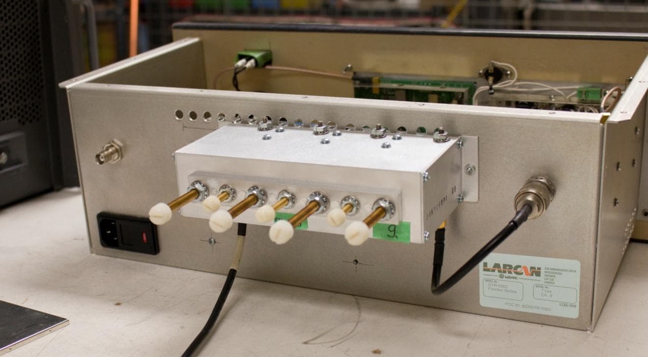
BZ5DTR10SC
Jun 16, 2014Digital Television Translator
Equipment Class
TBC - Licensed Broadcast Station Transmitter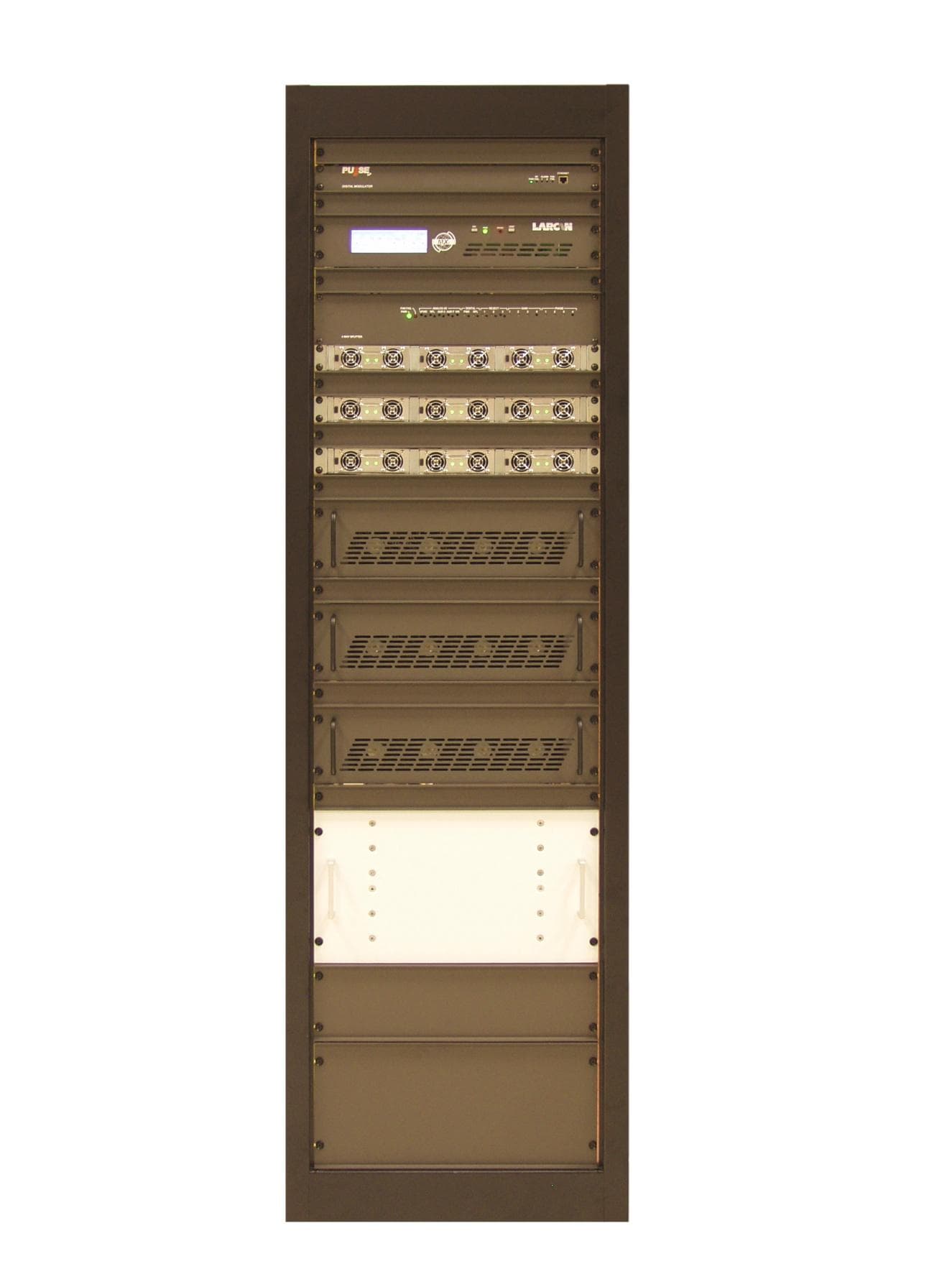
BZ5MXI1503U
Aug 04, 2013Television Broadcast Translator
Equipment Class
TBC - Licensed Broadcast Station Transmitter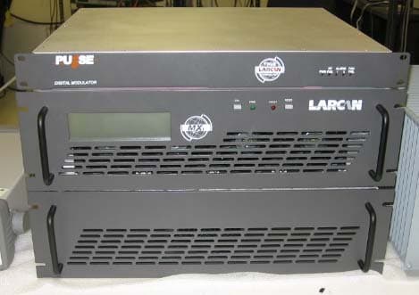
BZ5MXI501U
Nov 22, 2010Digital Television Broadcast Translator
Equipment Class
TBC - Licensed Broadcast Station TransmitterBZ5DTT250M
Jul 22, 2010Digital Television Broadcast Translator
Equipment Class
TBC - Licensed Broadcast Station Transmitter
BZ5MXI030U
Mar 09, 2010Digital Television Broadcast Translator
Equipment Class
TBC - Licensed Broadcast Station Transmitter