BZ5MXI1503UTelevision Broadcast Translator
Larcan Inc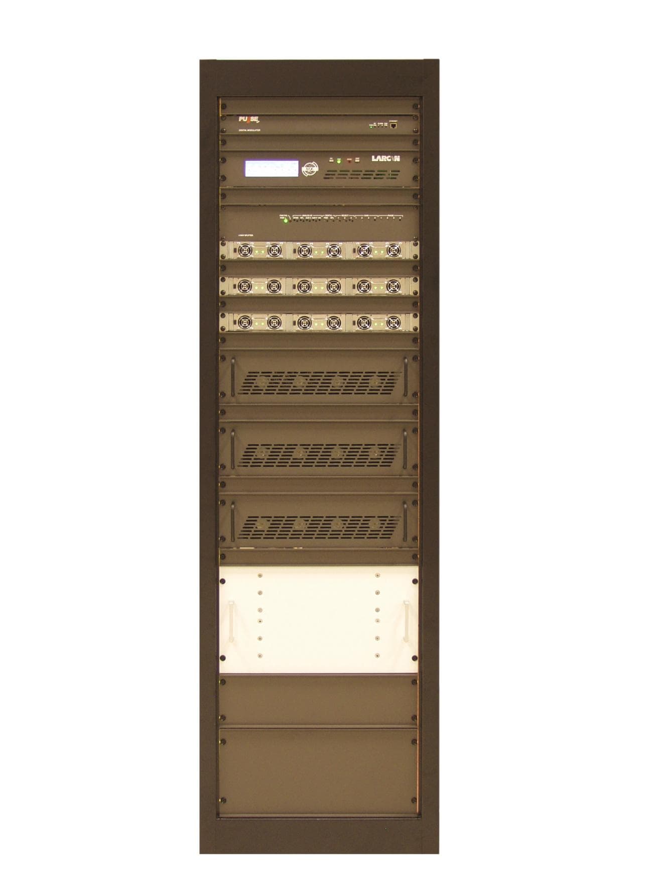
Click to zoom
Application Details
- Equipment Class
- TBC - Licensed Broadcast Station Transmitter
- Date of Grant
- Aug 04, 2013
- Application Purpose
- Original Equipment
- Date of Application
- Jun 12, 2013
- Equipment Note
- Television Broadcast Translator
- Frequency Range
- 470.00000000 - 608.00000000
- Company
- Larcan Inc
- Country
- Canada
Documents & Files
Document Text
Text extracted from the exhibit documents filed with the FCC. Open a document above to read the original.
Users Manual
PUB07-07 Rev 2 i TECHNICAL SERVICE MANUAL TRANSMITTER GENERAL INFORMATION LARCAN INC. 228 AMBASSADOR DRIVE MISSISSAUGA, ONTARIO CANADA L5T 2J2 PHONE: (905) 564-9222 FAX: (905) 564-9244 EMAIL: [email protected] PUB07-07 Rev 2 ii PUB07-07 GENERAL INFORMATION 1 INTRODUCTION.............................................................................................................................................................. 1 1.1 PRODUCTION CHANGES ................................................................................................................................................ 1 1.2 DISCLAIMER .................................................................................................................................................................. 1 1.3 CONTACT INFORMATION ............................................................................................................................................... 1 2 PREFIX NUMBERS .......................................................................................................................................................... 2 3 LARCAN PARTS, ASSEMBLIES, ASSEMBLY DRAWINGS AND SCHEMATIC NUMBERS ............................ 4 3.1 VENDOR STANDARD PART NUMBERS ........................................................................................................................... 4 3.2 LARCAN NUMBERS FOR PARTS, ASSEMBLIES AND DOCUMENTATION ......................................................................... 4 3.3 LEADED RESISTORS ...................................................................................................................................................... 4 3.4 SURFACE MOUNT RESISTORS 1/4W AND LESS .............................................................................................................. 5 3.5 SURFACE MOUNT CAPCITORS ....................................................................................................................................... 5 3.6 PARTS LISTS ................................................................................................................................................................. 6 4 SAFETY PRECAUTIONS ................................................................................................................................................ 7 4.1 BERYLLIUM OXIDE WARNING ....................................................................................................................................... 7 4.2 OTHER TOXIC MATERIALS ............................................................................................................................................ 7 4.3 DANGEROUS VOLTAGES ............................................................................................................................................... 7 4.4 SWITCH TO SAFETY ....................................................................................................................................................... 8 4.5 DISCOURAGE PESTS ...................................................................................................................................................... 9 APPENDIX A ........................................................................................................................................................................... 10 ABBREVIATIONS USED IN LARCAN INC. DOCUMENTS .............................................................................................................. 10 GENERAL INFORMATION PUB07-07 Rev 2 1 1 INTRODUCTION The transmitter technical details are described in this manual. The Manual is provided on this CD-ROM in PDF format. The complexity of the equipment and the amount of information requires this information to be presented in several publications. These publications are gathered into a single Volume to comprise the transmitter manual. The list of publications and their revision numbers is provided in separate PDF file TSM20-xxxG1 file. Mechanical assemblies are documented in this manual only as far as necessary to describe access to electronic subassemblies, such as circuit boards, thus, some mechanical items might be found only in a parts list. Those having assembly drawings in this manual also have a corresponding parts list. Numbers in circles on the assembly drawings refer to items identified as the parts list line or item number. 1.1 PRODUCTION CHANGES From time to time, it becomes necessary to make changes to the equipment described in this manual. Such changes are usually made either to provide improved performance or to accommodate component substitutions necessitated by vendor product availability. A revision number might follow the model or group number marked on the nameplate, chassis, or circuit board; or on a parts list. In a parts list, an "R" a number indicates the parts list revision status. This revision number should be quoted whenever contacting LARCAN Customer Service, especially if renewal parts are needed. 1.2 DISCLAIMER All material in this manual is copyright © LARCAN INC. as of the date of publication. Reproduction in whole or in part in any form for any purpose other than the exclusive use of the equipment owner without prior written authorization from LARCAN INC. is prohibited. Trademarks are the property of their respective owners and are mentioned in the text for discussion purposes only; any such mention is not an endorsement of the trademark or its owner. Parts lists may also contain trademarked vendor names as an aid in the procurement of spare parts. Every effort has been made to provide as much information about the equipment as possible and to ensure accuracy, however, LARCAN INC. assumes no responsibility and disclaims all liability for damages resulting from the use of this information or for any errors or omissions. These instructions do not assume to cover all possible details or variations in equipment n…
Text truncated - open the document above for the full version.
Users Manual
MXi501/1002U POWER AMPLIFIER HEATSINK ASSEMBLY CONTENTS 1 POWER AMPLIFIER HEATSINK ASSEMBLY..........................................................................................................1 2 FRONT END MODULE ASSEMBLY 21B1473G7........................................................................................................2 3 DRIVER MODULE 21B2708G3......................................................................................................................................3 4 PA PALLET ASSEMBLY 21B2729G1............................................................................................................................4 5 FIVE-WAY SPLITTER/FIVE-WAY COMBINER .......................................................................................................5 6 DIRECTIONAL COUPLER 21B2746G1........................................................................................................................6 7 BENCH TEST PROCEDURES........................................................................................................................................7 7.1 FRONT-END MODULE, 21B1473G7, BENCH TEST PROCEDURE....................................................................................7 7.2 DRIVER PALLET, 21B2708G3, BENCH TEST PROCEDURE.............................................................................................7 7.3 PA PALLET 21B2729G1 BENCH TEST PROCEDURE......................................................................................................7 FIGURES FIGURE 1 MXI SUB-ASSEMBLIES.................................................................................................................................................1 FIGURE 2 21B1473 MXI FRONT END UHF DTV DRIVER ASSEMBLY..........................................................................................8 FIGURE 3 11A1354 MXI FRONT END UHF DTV DRIVER SCHEMATIC.........................................................................................9 FIGURE 4 21B2708S DRIVER PALLET ASSEMBLY......................................................................................................................10 FIGURE 5 21B2708S DRIVER PALLET SCHEMATIC.....................................................................................................................11 FIGURE 6 21B2729A1 PALLET CIRCUIT ASSEMBLY...................................................................................................................12 FIGURE 7 21B2729S1 PALLET CIRCUIT SCHEMATIC..................................................................................................................13 FIGURE 8 21B2444A1 5 WAY SPLITTER ASSEMBLY..................................................................................................................14 FIGURE 9 21B2444S1 5 WAY SPLITTER SCHEMATIC..................................................................................................................15 FIGURE 10 21B2445A1 5 WAY COMBINER ASSEMBLY..............................................................................................................16 FIGURE 11 21B2445S1 5 WAY COMBINER SCHEMATIC.............................................................................................................17 FIGURE 12 21B2446S1 DIRECTIONAL COUPLER ASSEMBLY......................................................................................................18 FIGURE 13 21B2446S1 DIRECTIONAL COUPLER SCHEMATIC.....................................................................................................19 PUB11-014 Rev 1 July 2011 11-014-i MXi501/1002U Power Amplifier Heatsink Assembly MXi501/1002U POWER AMPLIFIER HEATSINK ASSEMBLY 1 POWER AMPLIFIER HEATSINK ASSEMBLY The MXi Power Amplifier Heatsink Assembly 41D2272G1 consists of a fan-cooled heatsink and ten printed circuit board sub-assemblies. The first module is a pre-amplifier, known as the Front-End Module. This first stage is operated in Class A mode. Next is the Driver pallet, which is biased so as to pre-correct for the non-linearity in the final amplifier stage. The next stage is a five-way splitter that splits the RF power so it can be fed to the PA pallets. The final amplifier stage is the PA pallets. After the pallets is the five-way combiner which combines the output power from the PA pallets. The last sub-assembly on the heatsink is the directional coupler which detects the forward and reflected power and provides samples to the control board and a RF test point on the rear panel. Also mounted on the heatsink is a thermal switch, which protects the amplifiers from over-temperature conditions such as the absent of cooling or amplifier over dissipation. This heatsink assembly is mounted in the Amplifier Chassis Assembly 41D2270G1 or G2. Descriptions of each stage are detailed in the following pages. Figure 1 MXi Sub-Assemblies The above picture illustrates the arrangement of the sub-assemblies on the amplifier heatsink assembly. From right to left are the Front-End and Driver modules. Centered and towards the back are the Splitter, PA modules and the Combiner. At the very back is the Directional Coupler. Strategically installed on the heatsink, is a thermal switch which protects the amplifier from over temperature conditions. Cooling for the heatsink is provided by a fan array assembly consisting of four 4-inch axial flow +12VDC muffin fans. This array is situated near the front section of the MXi housing underneath the MXi Amplifier Controller PC board. The fans blow air into the finned portion of the heatsink, which exhausts through the rear. PUB11-014 Rev 1 July 2011 11-014-1 MXi501/1002U Power Amplifier Heatsink Assembly MXi501/1002U POWER AMPLIFIER HEATSINK ASSEMBLY 2 FRONT END MODULE ASSEMBLY 21B1473G7 Drawing Reference: Figure 2 and Figure 3 The front end module performs several distinctive functions. Firstly, it serves as a pre-amplifier, which boosts the signal from the up-converter by …
Text truncated - open the document above for the full version.
Users Manual
AMPLIFIER CONTROLLER BOARD REV.5 PUB12-030 Rev. 1 Feb 14, 2013 12-030-i Amplifier Controller Board Rev.5 CONTENTS 1 INTRODUCTION ..................................................................................................................................................... 1 2 GENERAL OPERATIONS ...................................................................................................................................... 2 2.1 CONNECTOR AND SIGNAL DEFINITIONS ........................................................................................................................ 2 2.1.1 J1 BDM (Background Debug Mode) Connection ................................................................................................ 2 2.1.2 J2 Remote RS232 Connection .............................................................................................................................. 2 2.1.3 J3 Front Panel LCD and Touchpad ..................................................................................................................... 2 2.1.4 E20, E22 +50 Volt DC Power Supply .................................................................................................................. 2 2.1.5 J5 +50 Volt DC Power Supply Sensing (External) .............................................................................................. 2 2.1.6 J6 Remote Interface ............................................................................................................................................. 2 2.1.7 J7 – Not implemented ........................................................................................................................................... 3 2.1.8 J8 Fan Interface ................................................................................................................................................... 3 2.1.9 J9 External Controls ............................................................................................................................................ 3 2.1.10 J10 AGC Control ................................................................................................................................................. 3 2.1.11 J11 Not implemented ............................................................................................................................................ 3 2.1.12 J12 Forward RF Sample ...................................................................................................................................... 3 2.1.13 J13 Reflected RF Sample ..................................................................................................................................... 3 2.1.14 J14 Front Panel LCD Power ............................................................................................................................... 3 2.1.15 U25 RJ45 Ethernet Interface ............................................................................................................................... 3 2.2 JUMPER OPTIONS .......................................................................................................................................................... 4 2.2.1 Jumper E1–Serial Receive Data Select ................................................................................................................ 4 2.2.2 Jumper E2–Remote Control Reset ....................................................................................................................... 4 2.2.3 Jumper E3–Spare Line Configuration ................................................................................................................. 4 2.2.4 Jumper E4–External or Internal Power Supply Current Sensing ........................................................................ 4 2.2.5 Jumper E5–Front Panel ON/OFF Control Switch (System/Manual) .................................................................. 4 2.2.6 Jumper E6– Fan DC Power Select ...................................................................................................................... 4 2.2.7 Jumper E7–Manual Remote ON/OFF Control .................................................................................................... 5 2.2.8 Jumper E8–Power Supply Fan Interlock Bypass ................................................................................................. 5 2.2.9 Jumper E9–Forward RF Detector Color Burst Trap ........................................................................................... 5 2.2.10 Jumper E10–Forward RF Detector Sound Carrier Trap / DVB Filter ................................................................ 5 2.2.11 Jumper E11–Forward RF Detector Final Gain Control ..................................................................................... 5 2.2.12 Jumper E12– Reflected RF Detector Color Burst Trap ....................................................................................... 5 2.2.13 Jumper E13–Reflected RF Detector Sound Carrier Trap / DVB Filter ............................................................... 5 2.2.14 Jumper E14–Reflected RF Detector Final Gain Control ..................................................................................... 6 2.2.15 Jumper E15–Remote Manual Vswr Reset ............................................................................................................ 6 2.2.16 Jumper E16–AGC Disable Control ..................................................................................................................... 6 2.2.17 Jumper E17–VSWR Disable Control ................................................................................................................... 6 2.2.18 Jumper E23– P/S ON Status Polarity .................................................................................................................. 6 2.2.19 Jumper E24– P/S ON Command Polarity ............................…
Text truncated - open the document above for the full version.
Users Manual
41D2355 4-WAY SPLITTER UHF PUB13-01 Rev 0 Mar 4, 2013 i CONTENTS 1 GENERAL INFORMATION ........................................................................................................................................... 2 2 INPUTS AND OUTPUTS ................................................................................................................................................. 3 3 FRONT PANEL STATUS MONITORING .................................................................................................................... 5 4 DIGITAL FWD, RFL AND REJECT RF DETECTORS.............................................................................................. 6 4.1 CALIBRATION............................................................................................................................................................... 7 4.2 TROUBLESHOOTING...................................................................................................................................................... 7 5 ANALOG INTERNALLY DIPLEXED FWD, RFL AND AURAL RF DETECTORS.............................................. 8 5.1 CIRCUIT DESCRIPTION.................................................................................................................................................. 8 5.1.1 J18 Channel – Visual Forward............................................................................................................................ 8 5.1.2 J18 Channel – Aural Forward............................................................................................................................. 9 5.1.3 J19 Channel – Reflected ...................................................................................................................................... 9 5.1.4 Test and Calibration .......................................................................................................................................... 10 TEST EQUIPMENT.................................................................................................................................................................... 10 5.2 TEST PROCEDURE....................................................................................................................................................... 11 6 AMPLIFIER BALANCE ALIGNMENT ...................................................................................................................... 12 7 SPECIFICATION............................................................................................................................................................ 13 8 AMPLIFIERS TEST ......................................................................................................................................................... 1 LIST OF FIGURES FIGURE 1 4 WAY SPLITTER FRONT AND REAR VIEW.................................................................................................................... 3 FIGURE 2 4-WAY SPLITTER RF FLOW DIAGRAM 21B2917S1 SHT1 REV 0 ................................................................................... 4 FIGURE 3 4-WAY SPLITTER UHF SCHEMATIC 41D2355S1 REV 0 ................................................................................................ 5 FIGURE 4 4-WAY SPLITTER ASSEMBLY........................................................................................................................................ 6 FIGURE 5 4-WAY SPLITTER PCB SCHEMATIC 31C2007S1 SHT 1 REV 0 ....................................................................................... 7 FIGURE 6 4-WAY SPLITTER PCB SCHEMATIC 31C2007S1 SHT 2 REV 0 ....................................................................................... 8 FIGURE 7 4-WAY SPLITTER PCB SCHEMATIC 31C2007S1 SHT 3 REV 0 ....................................................................................... 9 FIGURE 8 4-WAY SPLITTER PCB SCHEMATIC 31C2007S1 SHT 4 REV 0 ..................................................................................... 10 FIGURE 9 4-WAY SPLITTER PCB SCHEMATIC 31C2007S1 SHT 5 REV 0 ..................................................................................... 11 FIGURE 10 4-WAY SPLITTER PCB SCHEMATIC 31C2007S1 SHT 6 REV 0 ................................................................................... 12 FIGURE 11 4-WAY SPLITTER PCB ASSEMBLY 31C2007A1 SHT 1 REV 0 .................................................................................... 13 41D2355 4-WAY SPLITTER UHF PUB13-01 Rev 0 Mar 4, 2013 2 1 GENERAL INFORMATION The Splitter is an intermediate RF Amplification stage employed in LARCAN UHF transmitters. A single 4-Way Splitter can be configured to drive from two to up to four higher power amplifiers. Typically, the signal level applied to the Splitter from the Modulator is between 0dBm and +5dBm (50 ohms). Every output gain and phase is adjustable from the front panel. The +12VDC Power Supply for the Splitter power stages is high efficiency switching supply. Power Supply is rated for 40W DC output power. Two 12VDC fans located on the left side panel of Splitter assembly provide enough air flow to cool down all four HELA10 RF amplifiers and other necessary circuits. Splitterr has built in three RF switches used for Modulator Switching and switching of RF Sense signals applied to Modulators for linear and nonlinear correction. +12VDC signal applied to the rear connector TELEMETRY pin 8 named ”RF SW2 ON/SEL MOD2” changes active connection from INPUT 1 to INPUT 2. 41D2355 4-WAY SPLITTER UHF PUB13-01 Rev 0 Mar 4, 2013 3 2 INPUTS AND OUTPUTS The 4-Way Splitter requires DC Power, a Control and Monitoring Interface, an RF input drive and an output connections to a higher power stages. Its inputs and outputs consist of the following: POWER IN: 2-Pin Connector J7 Pin Function 1 GND 2 +12VDC AC receptacle 6EGG1-1 has built–in holder for slow blow 2A fuse model 218002. MOD 1 IN and MOD 2 IN: SMA…
Text truncated - open the document above for the full version.
Users Manual
MXI1503-2004 CONTROL UNIT PUB13-09 Rev 1 i CONTENTS 1 INTRODUCTION.............................................................................................................................................................. 1 2 LCD GUI INTERFACE AND TOUCHPAD ................................................................................................................... 2 2.1 MAIN SCREEN AND TOUCHPAD OPERATIONS ................................................................................................................ 2 2.1.1 COMB Status LED ............................................................................................................................................... 3 2.1.2 AMPS Status LED ................................................................................................................................................ 3 2.1.3 COMSStatus LED ................................................................................................................................................ 3 2.1.4 LOG Status LED .................................................................................................................................................. 3 2.1.5 INTK Status LED ................................................................................................................................................. 3 2.1.6 REM Status LED .................................................................................................................................................. 4 2.1.7 ERR Status LED ................................................................................................................................................... 4 2.1.8 SubMenu Select Buttons ....................................................................................................................................... 4 2.2 COMBINED SCREEN ....................................................................................................................................................... 5 2.2.1 TRIP Status LED .................................................................................................................................................. 5 2.2.2 L/O Status LED .................................................................................................................................................... 5 2.2.3 RF Status LED ..................................................................................................................................................... 6 2.2.4 INTK Status LED ................................................................................................................................................. 6 2.2.5 PS OK Status LED ............................................................................................................................................... 6 2.2.6 COMSStatus LED ................................................................................................................................................ 6 2.2.7 AMPS Status LED ................................................................................................................................................ 7 2.2.8 SubMenu Select Buttons ....................................................................................................................................... 7 2.3 OVERALL AMPLIFIER SCREEN ....................................................................................................................................... 8 2.3.1 Individual Amplifier Screen ................................................................................................................................. 8 2.3.1.1. TRIP Status LED ............................................................................................................................................................... 9 2.3.1.2. L/O Status LED.................................................................................................................................................................. 9 2.3.1.3. INTK Status LED ............................................................................................................................................................ 10 2.3.1.4. PSOK Status LED ............................................................................................................................................................ 10 2.3.1.5. FAN1 Status LED ............................................................................................................................................................ 10 2.3.1.6. FAN2 Status LED ............................................................................................................................................................ 10 2.3.1.7. FAN3 Status LED ............................................................................................................................................................ 10 2.3.1.8. FAN4 Status LED ............................................................................................................................................................ 11 2.3.1.9. SubMenu Select Buttons .................................................................................................................................................. 11 2.3.2 Power Supply Submenu ..................................................................................................................................... 11 2.4 LOGS SCREEN ............................................................................................................................................................. 12 2.5 COMBINED INTERLOCKS SCREEN ................................................................................................................................ 12 2.5.1 AMP1 Interlock Status LED ..............................................…
Text truncated - open the document above for the full version.
Contact Information
Applicant
John E. Tremblay(Engineering, Vice President)
Technical Contact
LARCAN Inc.John E. Tremblay
[email protected]905 564 9222
228 Ambassador Drive · Mississauga, Ontario · Canada
Non-Technical Contact
LARCAN Inc.John E. Tremblay
[email protected]905 564 9222
Technical Specifications
| # | Rule Parts | Frequency Range | Power Output | Emission | Tolerance |
|---|---|---|---|---|---|
| 2 | 74 | 470 MHz - 608 MHz | 2000 W | 6M00K1D | 0.002 % |
Other Applications from Larcan Inc
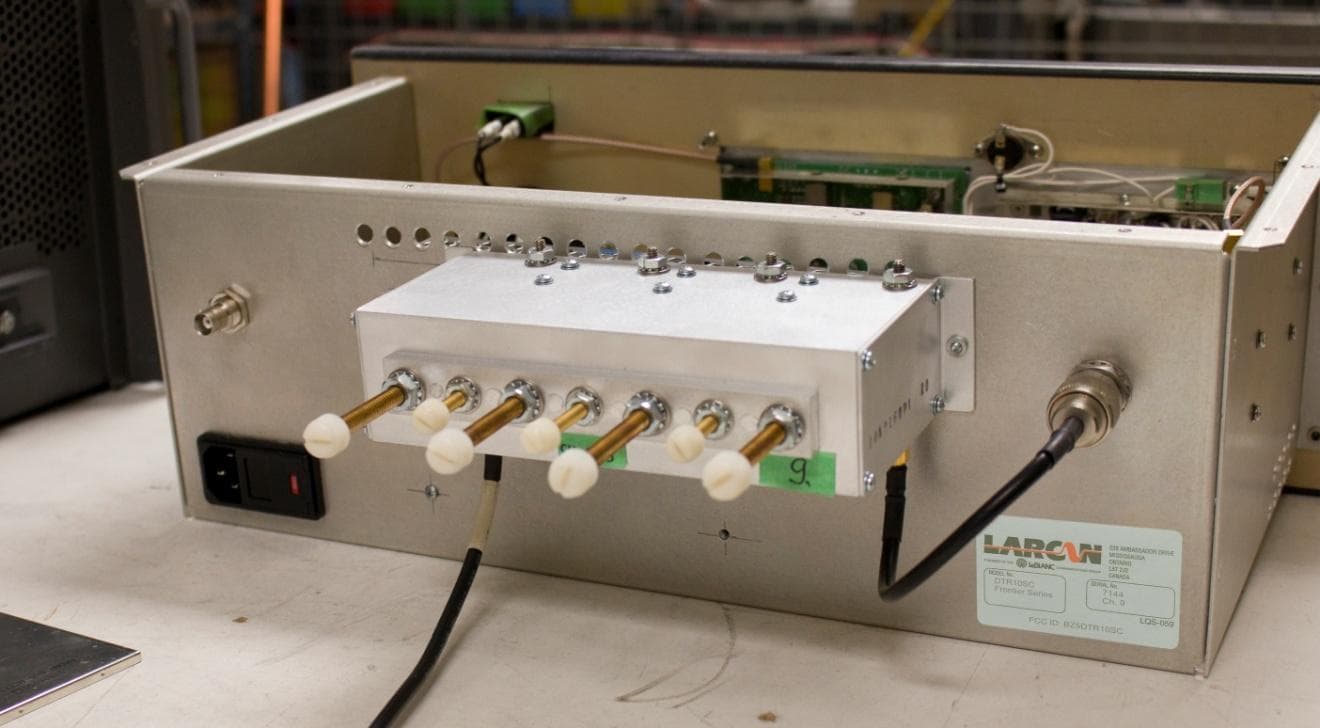
BZ5DTR10SC
Jun 16, 2014Digital Television Translator
Equipment Class
TBC - Licensed Broadcast Station Transmitter
BZ5MXI1002U
Jul 11, 2012Digital Television Translator
Equipment Class
TBC - Licensed Broadcast Station Transmitter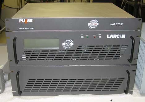
BZ5MXI501U
Nov 22, 2010Digital Television Broadcast Translator
Equipment Class
TBC - Licensed Broadcast Station TransmitterBZ5DTT250M
Jul 22, 2010Digital Television Broadcast Translator
Equipment Class
TBC - Licensed Broadcast Station Transmitter
BZ5MXI030U
Mar 09, 2010Digital Television Broadcast Translator
Equipment Class
TBC - Licensed Broadcast Station Transmitter