BZ5MXI501UDigital Television Broadcast Translator
Larcan Inc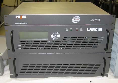
Click to zoom
Application Details
- Equipment Class
- TBC - Licensed Broadcast Station Transmitter
- Date of Grant
- Nov 22, 2010
- Application Purpose
- Original Equipment
- Date of Application
- Sep 23, 2010
- Equipment Note
- Digital Television Broadcast Translator
- Frequency Range
- 614.00000000 - 806.00000000
- Company
- Larcan Inc
- Country
- Canada
Documents & Files
Document Text
Text extracted from the exhibit documents filed with the FCC. Open a document above to read the original.
Users Manual
PSM20-374FB MXi501U TECHNICAL SERVICE MANUAL LARCAN INC. 228 AMBASSADOR DRIVE MISSISSAUGA, ONTARIO CANADA L5T 2J2 PHONE: (905) 564-9222 FAX: (905) 564-9244 EMAIL: [email protected] PSM20-374FB September 2010 MXI501U TECHNICAL SERVICE MANUAL CONTENTS PSM20-374FB MXi501U TECHNICAL SERVICE MANUAL 1 MXI501U AMPLIFIER INTRODUCTION ............................................................................................................. 1 2 SAFETY NOTICES .................................................................................................................................................... 2 2.1 BERYLLIUM OXIDE WARNING ........................................................................................................................................ 2 2.2 OTHER TOXIC MATERIALS ............................................................................................................................................. 2 2.3 DANGEROUS VOLTAGES ................................................................................................................................................. 2 2.3.1 Switch to Safety .................................................................................................................................................... 3 3 LARCAN PARTS, ASSEMBLIES, ASSEMBLY DRAWINGS AND SCHEMATIC NUMBERS ..................... 5 3.1 VENDOR STANDARD PART NUMBERS ............................................................................................................................ 5 3.2 LARCAN NUMBERS FOR PARTS, ASSEMBLIES AND DOCUMENTATION ......................................................................... 5 3.3 LEADED RESISTORS ........................................................................................................................................................ 6 3.4 SURFACE MOUNT RESISTORS 1/4W AND LESS ............................................................................................................... 6 3.5 SURFACE MOUNT CAPACITORS ...................................................................................................................................... 7 3.6 PARTS LISTS ................................................................................................................................................................... 7 3.6.1 Production Changes ............................................................................................................................................. 7 FIGURES FIGURE 1 MXI501U AMPLIFIER ASSEMBLY ................................................................................................................................. 1 FIGURE 2 MXI501U POWER SUPPLY ASSEMBLY .......................................................................................................................... 1 PUB07-025FB MXi501U OPERATIONS AND MAINTENANCE 1 MXI501U AMPLIFIER .................................................................................................................................................... 3 2 MXI501U AMPLIFIER HEATSINK ASSEMBLY ........................................................................................................ 4 3 MXi AMPLIFIER CONTROLLER ................................................................................................................................. 5 4 AMPLIFIER INSTALLATION AND STARTUP .......................................................................................................... 7 4.1 BEFORE APPLYING AC TO THE UNIT .............................................................................................................................. 7 4.2 APPLYING AC TO THE UNIT ........................................................................................................................................... 7 4.3 BEFORE TURNING THE AMPLIFIER ON ........................................................................................................................... 8 4.4 AMPLIFIER ON SEQUENCE ............................................................................................................................................. 8 4.4.1 Turning ON MXi Amplifier .................................................................................................................................. 9 4.4.2 TYPICAL DATA read on the LCD ....................................................................................................................... 9 5 TEST AND TROUBLESHOOTING ............................................................................................................................. 10 5.1 BENCH TEST PROCEDURES ........................................................................................................................................... 10 5.1.1 Front-End Module Bench Test Procedure ......................................................................................................... 10 5.1.2 IPA, 21B1324, Bench Test Procedure ................................................................................................................ 10 5.1.3 Driver, 21B1639, Bench Test Procedure ........................................................................................................... 11 5.1.4 PA Pallet 11A2142G1 Bench Test Procedure .................................................................................................... 11 5.2 BASIC TROUBLESHOOTING TECHNIQUES ...................................................................................................................... 12 5.2.1 No RF Output ..................................................................................................................................................... 12 5.2.2 Output Reduced to 56% ..................................................................................................................................... 12 6 MAINTENANCE ......................…
Text truncated - open the document above for the full version.
External Photos
BZ5MXI501UD Application for FCC Certification 500 Watt Digital Television Translator Exterior Photo:
ID Label/Location Info
228 Ambassador Drive Mississauga ON Canada L5T 2J2 November 8, 2010 Bette Taube Office of Engineering and Technology Re: FCC ID BZ5MXI501U Correspondence Reference number 39272 Ms. Taube: With regards to the discrepancies on the FCC Label/Location Info exhibit, I apologize for the typographical error on the sheet. The header should indeed read BZ5MXI501U and not BZ5MXI501UD. You will likely notice that this typo appears on the header of every exhibit. I have included the FCC Label/location exhibit, corrected to read properly. Sincerely, John Tremblay V. P. Engineering LARCAN U.S. Tel: 1-303-665-8000 Fax: 1-303-673-9900 Canada Tel: 1-905-564-9222 Fax: 1-905-564-9244 www.larcan.com Email: [email protected] BZ5MXI501U Application for FCC Certification 500 Watt Digital Television Translator FCC Label/Label & Location:
ID Label/Location Info
228 Ambassador Drive Mississauga ON Canada L5T 2J2 November 22, 2010 Bette Taube Office of Engineering and Technology Re: FCC ID BZ5MXI501U Correspondence Reference number 39312 Ms. Taube: With regards to the discrepancies on the FCC Label/Location Info exhibit, please find attached a revised label and location exhibit. If there is anything else you need please do not hesitate to contact me. Sincerely, John Tremblay V. P. Engineering LARCAN U.S. Tel: 1-303-665-8000 Fax: 1-303-673-9900 Canada Tel: 1-905-564-9222 Fax: 1-905-564-9244 www.larcan.com Email: [email protected] BZ5MXI501U Application for FCC Certification 500 Watt Digital Television Translator FCC Label/Label & Location:
Internal Photos
BZ5MXI501UD Application for FCC Certification 500 Watt Digital Television Translator Interior Photo of RF Amplifier:
Operational Description
BZ5MXI501UD Application for FCC Certification 500 Watt Digital Television Translator Operational Description: This application requests certification for a 500 Watt Digital Television Transmitter. The intended use of this digital translator is to rebroadcast a television relay station or other legal source of ATSC digital television signal. The MXi501U is a solid state digital regenerative translator designed to receive over-the- air ATSC signals, converting the RF signal to baseband digital format, processing the signal to eliminate noise, and then re-modulating, converting to the new broadcast channel, amplifying and filtering the signal before it is applied to the transmit antenna. The MXi501U may also be used as a Part74 transmitter by feeding an ATSC compliant transport stream to the input of the modulator directly. The receive section of the translator and the output modulation format conform to FCC Part 73.682(d), ATSC Digital Television Standards. The MXi501U consists of fiver components: a 1RU Pulse Modulator unit, and ATCS compliant transport stream receiver, a 3RU RF Power Amplifier; a 3RU Power supply and an output filter. The power supply and amplifiers employ integral cooling fans. The translator meets all FCC requirements for both the simple emissions mask and the stringent emissions mask. The output filter along with additional filtering within the amplifier provides more than 85dB of attenuation within the GPS Frequency bands (1164-1240 MHz and 1559-1610 MHz). Note that since these products are frequency agile in that they can be field tuned for different channels within the UHF television band, each unit has this filtering included, regardless of the channel. Testing results shown in this document were conducted on channel 30 (569MHz center frequency) with the exception of the frequency stability tests which were conducted on channel 29 (562MHz center frequency). These test results are representative of performance on any channel in the UHF broadcast spectrum. Wiring, shielding and construction are in accordance with accepted principles of good engineering practice. The translator’s construction is such that all hazardous components are enclosed or protected against accidental contact by operating personnel.
Parts List/Tune Up Info
BZ5MXI501UD Application for FCC Certification 500 Watt Digital Television Translator Parts List and Tune-up Procedure/Active Devices: The following is the procedure for changing the channel of the MXi501U translator. Since the amplifier is broadband, channel change involves retuning of the output filter and recalibration of the output meter. The amplifier meter was calibrated to read 100% (top scale) at full power and at the channel specified when the transmitter was tested at the factory. If the amplifier is to operate at a channel other than that of the factory test channel, the metering will require re-calibration. The power meter setting is a channel dependent calibration. 1. Connect the transmitter output to a 50 ohm dummy load or the antenna. The transmitter uses a 50Ω type N connector for its output. Calibrated directional coupler and suitable digital wattmeter should be used for measurements. 2. Connect the 208VAC mains input. This AC circuit should be rated for 15 amperes, and should be supplied through a slow-tripping breaker or time delay fuse. Generally, a breaker that is rated for across-the-line motor starting will be found to be satisfactory. Connect the power supply to the amplifier. 3. At this point the LCD screen should be illuminated, and the transmitter should be OFF. Depress the ON’ switch. The green LEDs should illuminate and the amplifier should be operating. The cooling fans on both the power supply and the amplifier should be running. 4. Attach the RF output power measuring device. 5. Turn down the drive level from the Transcoder (front end) before applying any RF input signal. 6. Slowly turn up the drive level until the output power reaches the desired level (on the power measuring device – not the transmitter power meter indication). 7. When the output power is at the desired level check that the voltage at TP3 (control PC board) is between 4.5V and 9.0VDC. 8. Adjust R48 until the voltage at TP3 is 4.0VDC. At this point the transmitter forward power meter should read 100%. 9. To calibrate the reflected power, install the jumper E17 (prevents VSWR trips). 10. Remove the cable from J12 at the control board and reconnect through a 10dB attenuator to J13. 11. The voltage measured at TP4 should be between 4.5V and 9.0VDC. 12. Adjust potentiometer R80 until the voltage at TP5 is 4.0VDC. At this point the reflected power should read 10%. 13. Reconnect the cables as they were, and remove jumper at E17. The output filter must be retuned as per the frequency response sweeps attached (note: two different tunings depending on the type of filter used). BZ5MXI501UD Application for FCC Certification 500 Watt Digital Television Translator Parts List and Tune-up Procedure: Mask Filter: In Band Insertion Loss BZ5MXI501UD Application for FCC Certification 500 Watt Digital Television Translator Parts List and Tune-up Procedure: Mask Filter: Input Return Loss BZ5MXI501UD Application for FCC Certification 500 Watt Digital Television Translator Parts List and Tune-up Procedure: Mask Filter: Out of Band Attenuation: BZ5MXI501UD Application for FCC Certification 500 Watt Digital Television Translator Active Devices List: ID Component Description Qty UM 31C1897G1 MXI CONTROLLER 1 EA CR1 1SMB9.0AT3 Zener Diode 9V sm 1 EA CR2 1SMB5.0AT3 DIODE 1 EA CR3 MURS120-T3 DIODE 1A 200V MARK U1D ONSEMI 1 EA CR4 HSMS-2800 DIODE SCHOTTKY HSMS-2800L30 1 EA CR5 HSMS-2820 DIODE SCHOTTKY HP MARM CO 1 EA CR6 1SMB5.0AT3 DIODE 1 EA CR7 MMSZ4678T1 DIODE ZENER 1.8V SM MKG-CC 0 EA CR8 HSMS-2800 DIODE SCHOTTKY HSMS-2800L30 1 EA CR9 HSMS-2820 DIODE SCHOTTKY HP MARM CO 1 EA CR10 1SMB5.0AT3 DIODE 1 EA CR11 MMSZ4678T1 DIODE ZENER 1.8V SM MKG-CC 0 EA CR12 MURS120-T3 DIODE 1A 200V MARK U1D ONSEMI 1 EA CR13 MURS120-T3 DIODE 1A 200V MARK U1D ONSEMI 1 EA CR14 MURS120-T3 DIODE 1A 200V MARK U1D ONSEMI 1 EA CR15 MURS120-T3 DIODE 1A 200V MARK U1D ONSEMI 1 EA CR16 MURS120-T3 DIODE 1A 200V MARK U1D ONSEMI 1 EA CR17 MURS120-T3 DIODE 1A 200V MARK U1D ONSEMI 1 EA ID Component Description Qty UM CR18 HSMS-2800 DIODE SCHOTTKY HSMS-2800L30 1 EA Q1 BC847BT/R TRANSISTOR, NPN 1 EA Q2 BC859CT/R TRANSISTOR, PNP 1 EA Q3 BC847BT/R TRANSISTOR, NPN 1 EA Q4 BC859CT/R TRANSISTOR, PNP 1 EA Q5 BC847BT/R TRANSISTOR, NPN 1 EA Q6 BC859CT/R TRANSISTOR, PNP 1 EA Q7 BC847BT/R TRANSISTOR, NPN 1 EA Q8 2N4351 TRANSISTOR FET N-CH SW 1 EA Q9 BC847BT/R TRANSISTOR, NPN 1 EA U1 MC68HC908GT8CFB IC Microcontroller 0 EA U1 MC68HC908GT16CFB IC Microcontroller 1 EA U2 MAX3110EEWI UART, -40°C to +85°C 28 Wide 1 EA U3 MOCD207 IC DUAL OPTO NAND S.M. 1 EA U4 MOCD207 IC DUAL OPTO NAND S.M. 1 EA U5 LM358D IC DUAL OP AMP SOIC 8 MOT 1 EA U6 MMPQ2222A TRANSISTOR NPN S.M. 1 EA U7 LM324D IC QUAD OP AMP SOIC 14 1 EA U8 MOCD207 IC DUAL OPTO NAND S.M. 1 EA U9 HXS 20-NP Current Transducer 1 EA U10 MMPQ2222A TRANSISTOR NPN S.M. 1 EA U11 LM339D IC COMPARITOR 1 EA U12 MOCD207 IC DUAL OPTO NAND S.M. 1 EA U13 LM324D IC QUAD OP AMP SOIC 14 1 EA U14 LM324D IC QUAD OP AMP SOIC 14 1 EA U15 LM324D IC QUAD OP AMP SOIC 14 1 EA U16 DS1867S-10 IC POT W/EEPROM DUAL 10K 16-SO 1 EA U17 LM324D IC QUAD OP AMP SOIC 14 1 EA U18 74HC00AD IC QUAD 2 INPUT NAND S.M. 1 EA U19 LM324D IC QUAD OP AMP SOIC 14 1 EA U20 LM358D IC DUAL OP AMP SOIC 8 MOT 1 EA VR1 78L05ACD Voltage Regulator Motorola 1 EA VR2 MC34064P5 MONITOR I.C. 1 EA VR3 MC7805BDT Voltage Regulator 5V 1A ONSemi 1 EA 21B1473G5 FRONT END (FOR DTV DRIVER) 1 EA Q1 MMBT2222ALT1 TRANSISTOR, MOTOROLA "1P" 1 EA U1 MHW9182 IC HYBRID AMP MOTOROLA 1 EA U2 LM358D IC DUAL OP AMP SOIC 8 MOT 1 EA U3 MC78M12CDT IC SEE 78M12CDT 1 EA U4 MC78L05ACD IC REGULATOR 100mA SOIC-8 1 EA CR1 BB811 DIODE VARACTOR 1 EA CR2 BB811 DIODE VARACTOR 1 EA CR3 HSMS-2850 DIODE HEWLETT PACKARD 1 EA 21B1951G1 IPA ASSY 1 EA U1 MC1723CD VOLTAGE LM723CD 1 EA Q3 MMBT2907ALT1 TRANSISTOR PNP MOTOROLA 2FE 1 EA CR100 MMBD7000LT1 DIODE DUAL GENERAL PURPOSE 1 EA CR110 MMBD7000LT1 DIODE DUAL GENERAL PURPOSE 1 EA BZ5MXI501UD Application for FCC Certification 500 Watt Digital Television Translator…
Text truncated - open the document above for the full version.
Schematics
MXi401U OPERATIONS AND MAINTENANCE PUB07-025 Rev 0 January 17, 2007 07-025-16 MXi401U Operations and Maintenance 8 TEST EQUIPMENT SETUP Figure 15 Test Equipment Setup Figure 5 41D2168 MXi401U/802U Amplifier Wiring Schematic sht1 Rev 0 Figure 9 21B1473 MXi Front End UHF DTV Driver Assembly sht1 Rev 5.1 Figure 10 11A1354 MXi Front End UHF DTV Driver Schematic sht1 Rev 2.1 ASSEMBLY - IPA FINAL UHF 21B1324 7 21B1324 7 Figure 11 21B1324 IPA Final Assembly sht1 Rev 7 Figure 12 21B1334S IPA Schematic Diagram sht1 Rev 0.1 Figure 13 21B1639S Driver Pallet Schematic sht1 Rev 5 Figure 14 11A2142A1S Pallet Ci rcuit Schematic sht1 Rev 3 Figure 15 21B2425A1 4 Way Splitter Assembly sht1 Rev 0 Figure 16 21B2425S1 4 Way Splitter Schematic sht1 Rev 0 Figure 17 21B2425A1 4 Way Combiner Assembly sht1 Rev 0 Figure 18 21B2425S1 4 Way Comb iner Schematic sht1 Rev 0 Figure 4 11A2226S1 MXi401 Current Sensor Schematic sht1 Rev 1 Figure 5 41D2185 MXi401 Power Supply Chassis Wiring Schematic sht1 Rev 0 Figure 23 MXi Controller Board Assembly Diagram 31C1897A2 sht1 Rev 2.2 Figure 24 MXi Controller Board Schematic 31C1897S1 sht1 Rev 2.3 Figure 25 MXi Controller Board Schematic 31C1897S2 sht2 Rev 2.3 Figure 26 MXi Controller Board Schematic 31C1897S3 sht3 Rev 2.3 Figure 27 MXi Controller Board Schematic 31C1897S4 sht4 Rev 2.3 Figure 28 MXi Controller Board Schematic 31C1897S5 sht5 Rev 2.3
Test Report
BZ5MXI501UD Application for FCC Certification 500 Watt Digital Television Translator Spurious Emissions (Simple Mask): BZ5MXI501UD Application for FCC Certification 500 Watt Digital Television Translator Spurious Emissions (Stringent Mask): BZ5MXI501UD Application for FCC Certification 500 Watt Digital Television Translator Spurious Emissions:
Test Report
BZ5MXI501UD Application for FCC Certification 500 Watt Digital Television Translator Cabinet Radiation BZ5MXI501UD Application for FCC Certification 500 Watt Digital Television Translator Cabinet Radiation:
Test Report
BZ5MXI501UD Application for FCC Certification 500 Watt Digital Television Translator Frequency Drift versus Temperature: Readings Calculation Pilot Frequency Deviation % from ref. Temp (°C) VAC= 102 120 138 (Hz) -30 650307355650307400650307318 5704 0.00087712 -20 650310662650310662650310662 2360 0.00036290 -10 650312589650312589650312589 433 0.00006658 0 650313359650313359650313359 337 0.00005182 10 650314072650314072650314070 1050 0.00016146 20 650313022650313022650313022 0 0.00000000 30 650311757650311767650311750 1272 0.00019560 40 650310711650310750650310721 2311 0.00035537 50 650310037650310037650310037 2985 0.00045901 60 650310775650310775650310775 2247 0.00034553 Test Setup for Frequency Stability Measurements: Test Equipment List: • Thermostatically-controlled Temperature Chamber – Cincinnati Sub-Zero • HP 8594E Spectrum Analyzer, S/N 3303A00399
Test Report
BZ5MXI501UD Application for FCC Certification 500 Watt Digital Television Translator Power Measurements: The translator’s power meter circuit uses a detected sample from a coupler on the output. An averaging detector circuit provides the DC level to drive the translator’s output level meter. The translator was connected to a test load through a calibrated directional coupler. The spectrum analyzer’s “Channel Power” function was used to measure the average power level of the signal as sampled through the directional coupler. (See figure below). Measured power: 19.4dBm Coupling and cable loss: 37.6dBm Power: 57.0dBm Power: 500 Watts
Test Report
BZ5MXI501UD Application for FCC Certification 500 Watt Digital Television Translator Attenuation Characteristics:
Test Report
BZ5MXI501UD Application for FCC Certification 500 Watt Digital Television Translator Digital Signal: Eye Diagram/Signal to Noise Ratio/Error Vector Magnitude BZ5MXI501UD Application for FCC Certification 500 Watt Digital Television Translator Digital Signal: Group Delay/Frequency Response
Test Setup Photos
BZ5MXI501UD Application for FCC Certification 500 Watt Digital Television Translator Test Setup Photo: Block Diagram of Test Setup: Test Equipment: Instrument Make/Model Serial # Last Calibration Date Spectrum Analyzer HP8594E 3303A00399 Dec. 3, 2003 Signal Analyzer Tektronix RFA300 B010126 Feb. 6, 2003 RF Power Meter Agilent 8712ET US40371604Mar. 6, 2000
Contact Information
Applicant
John E. Tremblay(Engineering, Vice President)
Technical Contact
LARCANJohn Tremblay
[email protected]905 564 9222
228 Ambassador Drive · Mississauga, Ontario · Canada
Non-Technical Contact
LARCANJohn Tremblay
[email protected]905 564 9222
Technical Specifications
| # | Rule Parts | Frequency Range | Power Output | Emission | Tolerance |
|---|---|---|---|---|---|
| 2 | 74 | 614 MHz - 806 MHz | 500 W | 6M00K1D | 0.002 % |
Other Applications from Larcan Inc
BZ5DTR10SC
Jun 16, 2014Digital Television Translator
Equipment Class
TBC - Licensed Broadcast Station Transmitter
BZ5MXI1503U
Aug 04, 2013Television Broadcast Translator
Equipment Class
TBC - Licensed Broadcast Station Transmitter
BZ5MXI1002U
Jul 11, 2012Digital Television Translator
Equipment Class
TBC - Licensed Broadcast Station TransmitterBZ5DTT250M
Jul 22, 2010Digital Television Broadcast Translator
Equipment Class
TBC - Licensed Broadcast Station Transmitter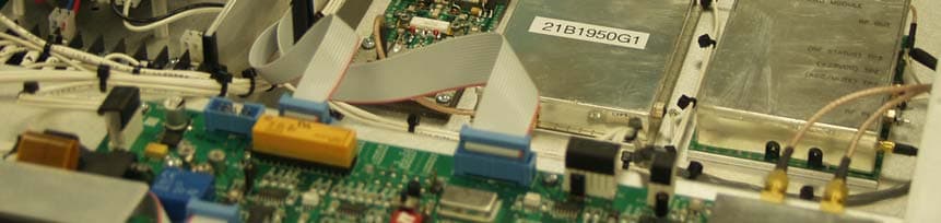
BZ5MXI030U
Mar 09, 2010Digital Television Broadcast Translator
Equipment Class
TBC - Licensed Broadcast Station Transmitter