E675JS0032CONTINUOUS DUTY POWER AMPLIFIER
Powerwave Technologies Inc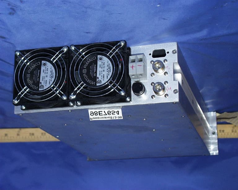
Click to zoom
Application Details
- Equipment Class
- AMP - Amplifier
- Date of Grant
- Feb 09, 2000
- Application Purpose
- Original Equipment
- Date of Application
- Nov 18, 1999
- Equipment Note
- CONTINUOUS DUTY POWER AMPLIFIER
- Frequency Range
- 850.00000000 - 870.00000000
- Company
- Powerwave Technologies Inc
- Country
- United States
Documents & Files
Document Text
Text extracted from the exhibit documents filed with the FCC. Open a document above to read the original.
Users Manual
044-05040 Rev. A INSTALLATION & SERVICE MANUAL MODEL K-10 CONTINUOUS DUTY POWER AMPLIFIER 850-870 MHz 25 June 1998 Powerwave Technologies, Inc. Tel: 949-757-0530 2026 McGaw Avenue Fax: 949-757-0941 Irvine, CA 92614 Web Site: www.pwav.com 044-05040 Rev. A ii TABLE OF CONTENTS Par. Section 1 Page No. General Description No. 1-1 Introduction......................................................................................................................1-1 1-2 General Description.........................................................................................................1-1 1-3 Functional and Physical Specifications............................................................................1-1 1-4 Equipment Changes........................................................................................................1-1 1-5 Ordering Information........................................................................................................1-2 Section 2 Installation 2-1 Introduction......................................................................................................................2-1 2-2 Electrical Service Recommendations..............................................................................2-1 2-3 Unpacking and Inspection...............................................................................................2-1 2-4 Installation Instructions....................................................................................................2-2 2-5 Amplifier Module Alarm and Control Connector..............................................................2-2 Section 3 Operating Instructions 3-1 Introduction......................................................................................................................3-1 3-2 Location and Function of Amplifier Module Control and Indicators.................................3-1 3-3 Initial Start-Up and Operating Procedures.......................................................................3-3 3-4 Variable Input Switch.......................................................................................................3-3 Section 4 Principles of Operation 4-1 Introduction......................................................................................................................4-1 4-2 RF Input Signal................................................................................................................4-1 4-3 RF Output Load...............................................................................................................4-1 4-4 Functional Description.....................................................................................................4-1 4-5 K10 Amplifier Module.......................................................................................................4-3 4-5.1 Main Amplifier..................................................................................................................4-3 4-5.2 Loop Control....................................................................................................................4-3 4-5.3 Amplifier Monitoring.........................................................................................................4-3 4-5.4 Amplifier Module Cooling.................................................................................................4-3 4-6 Power Distribution............................................................................................................4-4 044-05040 Rev. A iii TABLE OF CONTENTS (Continued) Section 5 Maintenance 5-1 Introduction......................................................................................................................5-1 5-2 Periodic Maintenance......................................................................................................5-1 5-3 Test Equipment Required for Test...................................................................................5-1 5-4 Cleaning air Inlets/Outlets................................................................................................5-2 5-5 Performance Test............................................................................................................5-2 5-5.1 Amplifier Performance Test.............................................................................................5-2 5-6 Field Replaceable Parts and Modules.............................................................................5-4 5-6.1 K10 Power Amplifier Module...........................................................................................5-4 5-6.2 Cooling Fans....................................................................................................................5-4 5-6.3 Fuse.................................................................................................................................5-4 Section 6 Troubleshooting 6-1 Introduction......................................................................................................................6-1 6-2 Troubleshooting...............................................................................................................6-1 6-3 Return for Service Procedure..........................................................................................6-2 6-3.1 Obtaining an RMA...........................................................................................................6-2 6-3.2 Repackaging for Shipment..............................................................................................6-2 LIST OF ILLUSTRATIONS Figure Page No. No. 1-1 Five K10 Amplifiers in Subrack........................................................................................1-3 2-1 Alarm and Control Connector (on Rear of K10 Module)..................................................2-2 2-2 K10 Amplifier, Rear view........................................................................................…
Text truncated - open the document above for the full version.
Block Diagram
PowerWave: 850-870 MHz 90W Power Amplifier line-up KTC1/21/98 Specifications:MinTypMaxUnitAlarms indicators Frequency 850.00860.00870.00MHzPWR ON Output Power90.00WattsOVRTEMP Input Power0.2525.00WattsLOW INPUT PWR Input Return Loss -14.00dBHIGH INPUT PWRMRF184 Gain10.0030.00dBLOW PWR Calculate Junction Temperature (C)=Tc+Pd*Rjc=99.87at +25C Supply Voltage26.0028.0030.00VHIGH VSWRAssume case temp@25C=50.00134.87at +60C Total Current11.40ATheta jc=1.1C/W1.10 Efficiency36.00%Notes:Yellow box is for inputA+ (V)28.00 Red highlighted number is calculated, cannot modify.I (A)3.50 MIMICPo (W)55.00 Input PowerSNA-386/11dBmPin (W)2.34 0.25WGain 23.98dBm21.00 DRIVER BOARDPALLET 184COMBINER/OUTPUT BOARD AnarenAnaren Detector Voltage3dB hybrid combiner loss3dB hybrid combiner loss -0.30dB-0.30dB Fixed High Power Pad2.19Watts54.95Watts -20.00dBCoupling3.9833.40dBm47.40dBm -10.006.00MIMIC AttenuatorVariableVariableSNA-286/13dBmRFMD2132/33dBmPredriverLow Pass FilterWattmeter PI networkAttenuatorPI PadAttenuatorGainGainGain-0.30dB-0.25dB -6.00-2.98-8.00dB-7.3015.00dB28.00dB14.00dBDriver 1 Gain 14.00dB 2.50mW0.63mW0.320.050.010.30mW0.19Watts4.68Watts 3.98dBm-2.02dBm-5.00-13.00-20.30-5.30dBm22.70dBm36.70dBmDriver 2Output Power 102.33Watts95.50Watts90.16Watts AGC 50.10dBm49.80dBm49.55dBm Pad, dBPo, W -6.30113.002.19Watts54.95Watts -7.3090.0033.40dBm47.40dBmTX_VFWDTX_VRVD -8.3072.00 -9.3057.00 DIP Gain/LossPinPoutPinPoutUsageCombiner/Splitter Way PinSWITCHAttenuatorDescriptiondBWattWattdBmdBm 0.251.00-6.00Output Power0.0090.1690.1649.5549.551.00 0.502.00-9.00Wattmeter-0.2595.5090.1649.8049.551.00 1.003.00-12.00Low Pass Filter-0.30102.3395.5050.1049.801.00 2.004.00-15.003dB hybrid combiner-0.3054.95102.3347.4050.101.002.00 4.005.00-18.00Driver14.002.1954.9533.4047.402.00 8.006.00-21.003dB hybrid splitter-0.304.682.1936.7033.401.002.00 16.007.00-24.00Predriver14.000.194.6822.7036.701.00 25.008.00-26.00RFMD2132/33dBm28.000.000.19-5.3022.701.00 SNA-286/13dBm15.000.000.00-20.30-5.301.00 Variable Attenuator-7.300.000.00-13.00-20.301.00 PI Pad-8.000.000.00-5.00-13.001.00 Variable Attenuator-2.980.000.00-2.02-5.001.00 PI Attenuator-6.000.000.003.98-2.021.00 Fixed High Power Pad-20.000.250.0023.983.981.00 Input Power0.000.250.2523.9823.981.00 Total Gain (dB)25.57 Figure 4-2. K10 Block diagram
ID Label/Location Info
PROPOSED FCC ID LABEL FORMAT Applicant: POWERWAVE TECHNOLOGIES, INC. 2026 McGAW AVENUE IRVINE, CA 92614 Model: K-10 FCC ID: E675JS0032 POWERWAVE TECHNOLOGIES FCC ID: E675JS0032 This device complies with part 15 of the FCC Rules. Operation is subject to the following two conditions: (1) This device may not cause harmful interference, and (2) this device must accept any interference received, including interference that may cause undesired operation. FCC ID LABEL AREA
Test Report
FCC CFR47 PART 90 CERTIFICATION TEST REPORT FOR SINGLE CHANNEL100W AMPLIFIERS MODEL: K-10 FCC ID: E675JS0032 REPORT NUMBER: 98E7654 ISSUE DATE: AUGUST 7,1998 Prepared for POWERWAVE TECHNOLOGIES, INC. 2026 McGAW AVENUE IRVINE, CA 92614 USA Prepared by COMPLIANCE CERTIFICATION SERVICES, INC. 1366 BORDEAUX DRIVE SUNNYVALE, CA 94089, USA TEL: (408) 752-8166 FAX: (408) 752-8168 REPORT NO: 98E7654 DATE: AUGUST 7, 1998 FCC ID: E675JS0032EUT: SINGLE CHANNEL 100W AMPLIFIER 0 COMPLIANCE CONSULTING SERVICES DOCUMENT NO:CCSUP4031A 1366 BORDEAUX DRIVE SUNNYVALE, CA 94089 USA TEL:(408) 752-8166 FAX:(408) 752-8168 This report shall not be reproduced except in full, without the written approval of CCS. TABLE OF CONTENTS PAGE 1. FCC CERTIFICATION INFORMATION.........................................................................................1 2. VERIFICATION OF COMPLIANCE...............................................................................................3 3. TEST FACILITY...............................................................................................................................4 4. ACCREDITATION AND LISTING..................................................................................................4 5. MEASUREMENT INSTRUMENTATION.......................................................................................4 6. MEASURING INSTRUMENT CALIBRATION..............................................................................4 7. UNITS OF MEASUREMENT...........................................................................................................4 8. CLASSIFICATION OF DIGITAL DEVICE.....................................................................................5 9. RADIATED EMISSION LIMITS......................................................................................................6 10. RADIATED EMISSION TEST PROCEDURE.................................................................................7 11. CONDUCTED EMISSION LIMITS.................................................................................................7 12. AMBIENT CONDITIONS.................................................................................................................8 13. EQUIPMENT MODIFICATIONS.....................................................................................................8 14. TEST EQUIPMENT LIST.................................................................................................................9 15. EUT SETUP PHOTOS.....................................................................................................................10 17. EXTERNAL I/O CABLE CONSTRUCTION DESCRIPTION......................................................14 18. CONFIGURATION BLOCK DIAGRAM.......................................................................................15 19. FCC PART 2 CERTIFICATION TEST RESULTS:.......................................................................16 SECTION 2.1046 RF POWER OUTPUT.............................................................................................................16 SECTION 2.1047 MODULATION CHARACTERISTICS..................................................................................17 SECTION 2.1049 OCCUPIED BANDWIDTH.....................................................................................................17 SECTION 2.1051 SPURIOUS EMISSION AT ANTENNA TERMINALS.........................................................19 SECTION 2.1053 FIELD STRENGTH OF SPURIOUS RADIATION................................................................21 SECTION 2.1055 FREQUENCT STABILITY......................................................................................................25 ATTACHMENT 1. EUT PHOTOGRAPHS 2. INSTALLATION & SERVICE MANUAL 3. ADDENUM 1 SCHEMATIC & PARTS LISTS 4. PROPOSED FCC ID LABEL FORMAT REPORT NO: 98E7654 DATE:AUGUST 7, 1998 FCC ID: E675JS0032 EUT: SINGLE CHANNEL 100W AMPLIFIER 1 COMPLIANCE CERTIFICATION SERVICES DOCUMENT NO:CCSUP4031A 1366 BORDEAUX DRIVE SUNNYVALE, CA 94089 USA TEL:(408) 752-8166 FAX:(408) 752-8168 This report shall not be reproduced except in full, without the written approval of CCS. 1. FCC CERTIFICATION INFORMATION The following information is in accordance with FCC Rules, 47CFR Part2, Sections 2.1033 – 2.1057. Section 2.1033 (1) Applicant/Manufacturer: POWERWAVE TECHNOLOGIES, INC. 2026 McGAW AVENUE IRVINE, CA 92614 Contact person: JEFF DALE Telephone number: (949)809-1466 (2) FCC ID: E675JS0032, Model: K-10 (3) Instructions/Installation Manual :Refer to Attachment: Installation and Service manual. (4) Type of Emissions: F3E (5) Frequency Range: Power Amplifier: 850 – 870MHz (6) Maximum Power Rating: 100 Watts (7) Maximum power rating as defined in Section 90.635(b): < 500Watts. (8) Applied voltage and currents into the final transistor elements: Refer to Attachment: Schematics and Parts list. Confidentiality is requested for these items. (9) Tune-up Procedure: Refer to Attachment: Installation and Service manual. (10) Function of Each Active Device ITEM P-WAVE PART NO. VENDOR VENDOR PART NO. QTY PART NAME 1 925-00017-002 MINI CKTS ERA-2SM 1 MIC AMP. 2 925-00035-001 MINI CKTS ERA-5SM 1 MIC AMP 3 924-00028-001 MOTOROLA MRF184 2 TRANSISTOR 4 924-00019-001 MOTOROLA MRF182 1 TRANSISTOR Complete Circuit Diagrams and Functional Diagram Refer Attachment: Schematics and Parts list. Confidentiality is requested for these items. REPORT NO: 98E7654 DATE:AUGUST 7, 1998 FCC ID: E675JS0032 EUT: SINGLE CHANNEL 100W AMPLIFIER 2 COMPLIANCE CERTIFICATION SERVICES DOCUMENT NO:CCSUP4031A 1366 BORDEAUX DRIVE SUNNYVALE, CA 94089 USA TEL:(408) 752-8166 FAX:(408) 752-8168 This report shall not be reproduced except in full, without the written approval of CCS. Means for Frequency Stabilization: Not Applicable. Eut is a power amplifier Means for Limiting Modulation: Not Applicable. Eut is a power amplifier Means for Limiting Power: Not Applicable. Mea…
Text truncated - open the document above for the full version.
Contact Information
Applicant
Jeff Dale(Principal Reliability Engineer)
Technical Contact
COMPLIANCE ENGINEERING SERVICES, INC.MIKE KUO
[email protected]408-752-8166
1366 BORDEAUX DRIVE · SUNNYVALE, California · United States
Non-Technical Contact
COMPLIANCE ENGINEERING SERVICES, INC.MIKE KUO
[email protected]408-752-8166
Test Firm
Compliance Certification Services IncSteve Cheng
Technical Specifications
| # | Rule Parts | Frequency Range | Power Output | Emission |
|---|---|---|---|---|
| 1 | 90 | 850 MHz - 870 MHz | 100 W | F3E |
Other Applications from Powerwave Technologies Inc
E675JS0123
Nov 03, 2011Multi-carrier RF Power Amplifier
Equipment Class
AMP - Amplifier
E675JS0120
Aug 26, 2010Nexus Dual Band Repeater
Equipment Class
TNB - Licensed Non-Broadcast Station Transmitter
E675JS0119
Aug 01, 2010Nexus Dual Band Repeater
Equipment Class
PCB - PCS Licensed Transmitter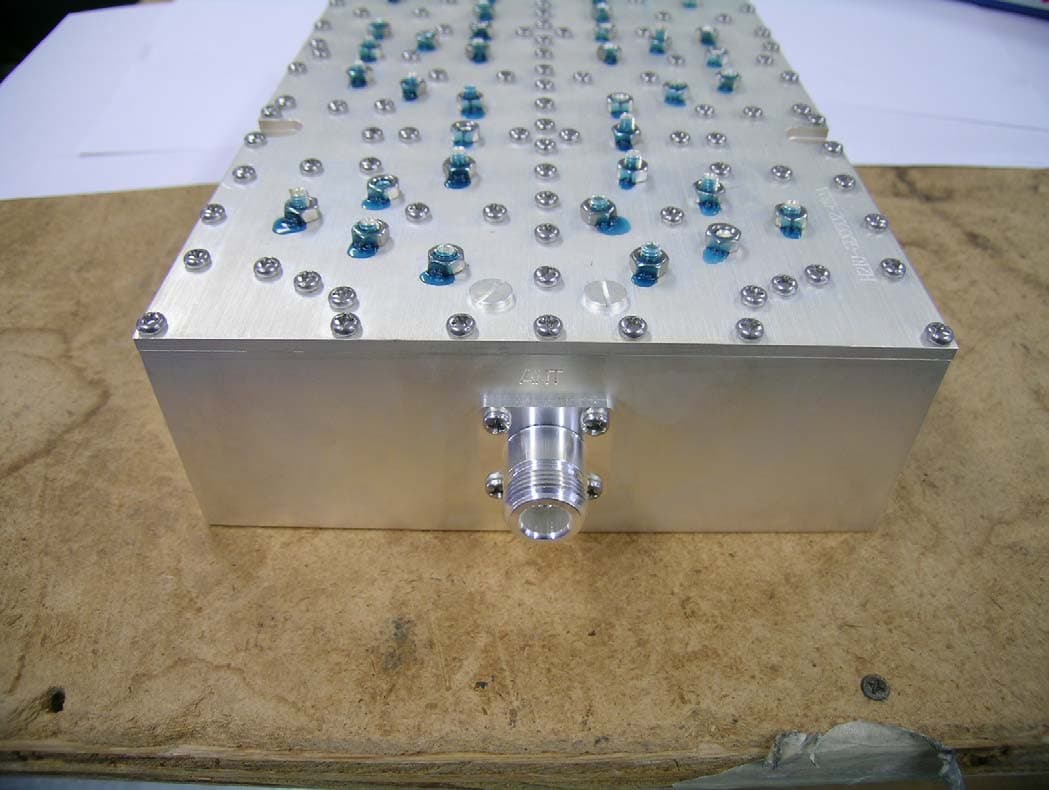
E675JS0118
Jul 26, 2010Nexus Dual Band Repeater
Equipment Class
PCB - PCS Licensed Transmitter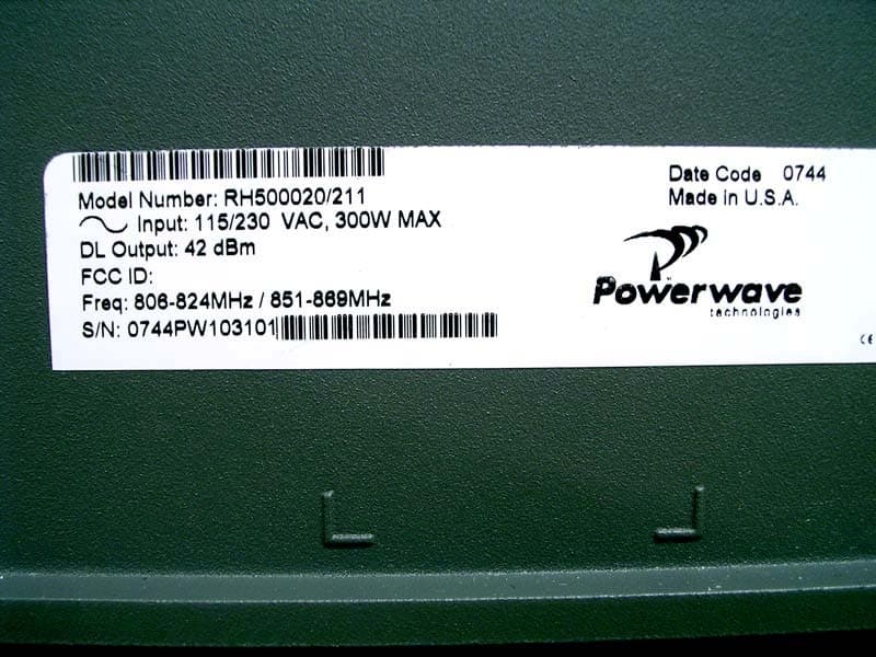
E675JS0096
Jan 10, 2008Wideband Radio Head
Equipment Class
TNB - Licensed Non-Broadcast Station Transmitter