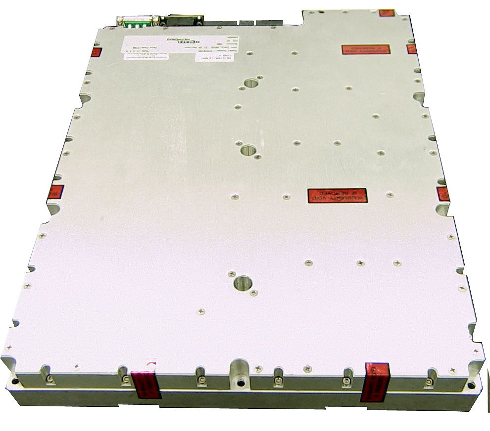
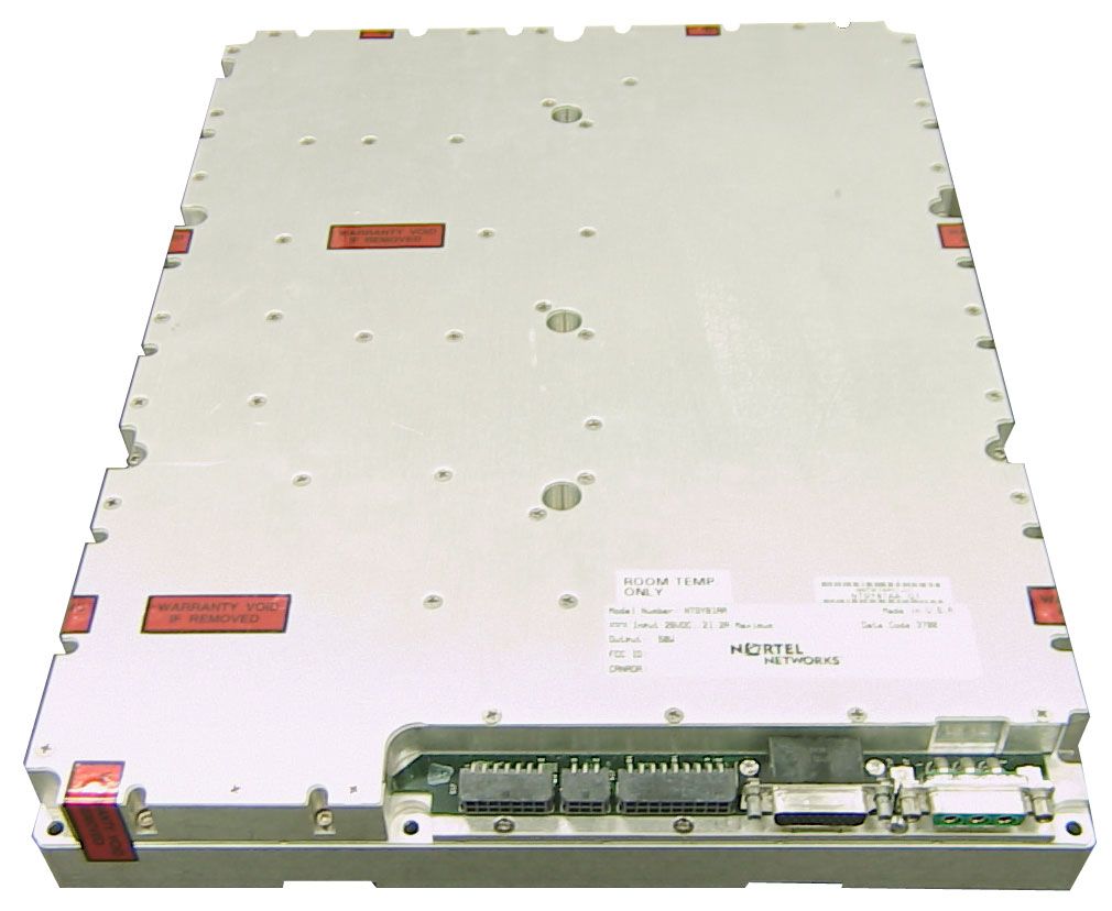
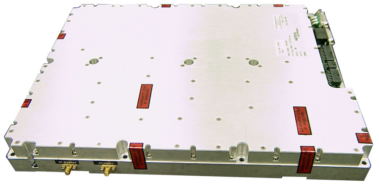
E675JS0046Hurricane, Model NTGY81AA
Powerwave Technologies Inc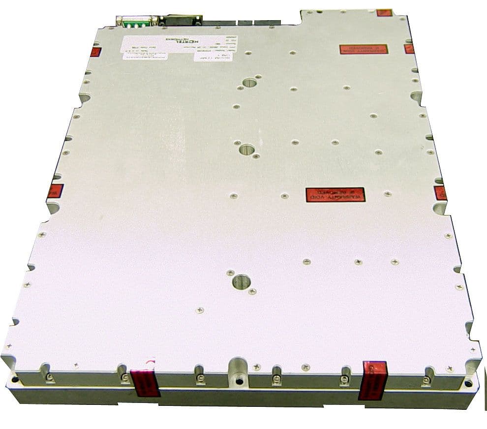
Click to zoom
Application Details
- Equipment Class
- AMP - Amplifier
- Date of Grant
- Nov 20, 2000
- Application Purpose
- Original Equipment
- Date of Application
- Nov 15, 2000
- Equipment Note
- Hurricane, Model NTGY81AA
- Frequency Range
- 1930.00000000 - 1990.00000000
- Company
- Powerwave Technologies Inc
- Country
- United States
Documents & Files
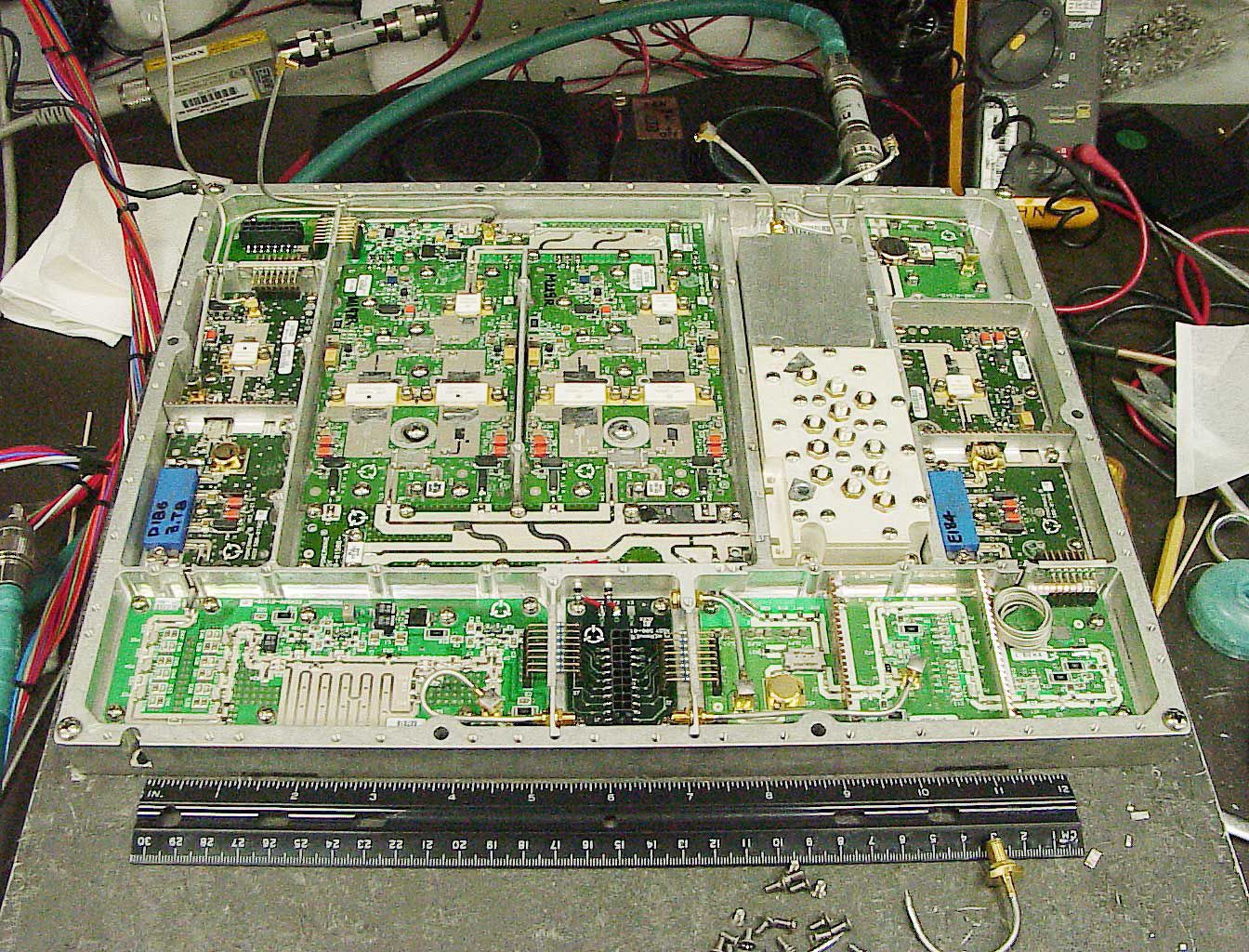
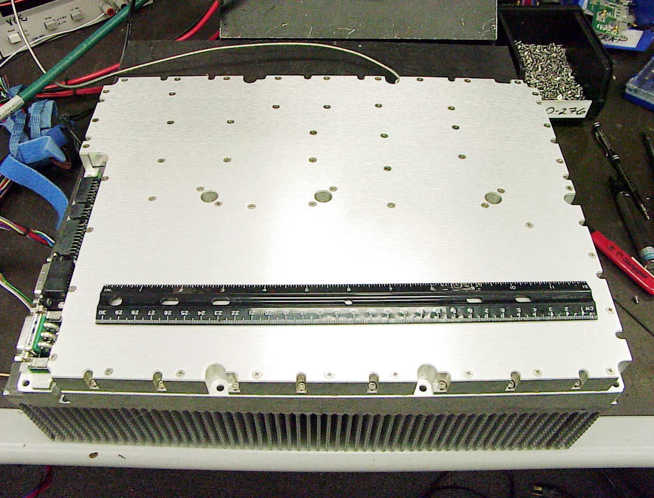
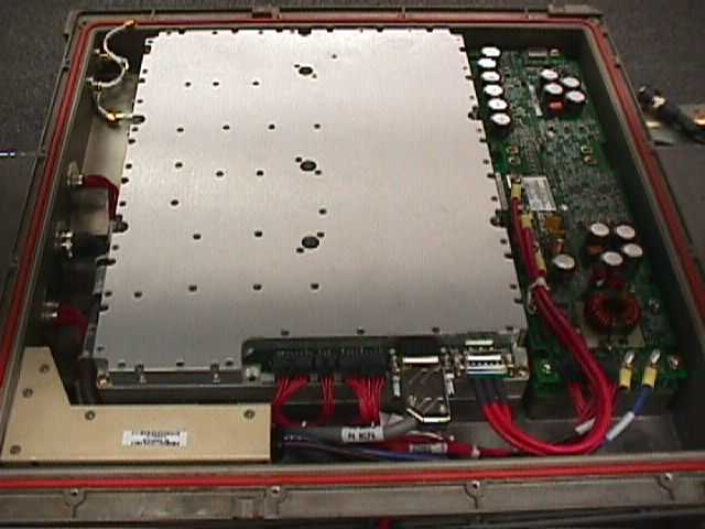
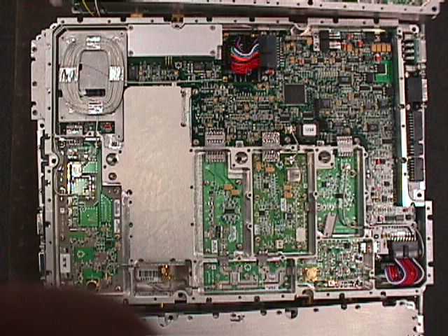
Document Text
Text extracted from the exhibit documents filed with the FCC. Open a document above to read the original.
Users Manual
044-05079 Rev. A INSTALLATION & SERVICE MANUAL MULTICHANNEL POWER AMPLIFIER NTGY81AA 1930-1990 MHz 50 WATTS AVERAGE POWER 07 September 2000 2 Powerwave Technologies, Inc.Tel: 949-809-1100 2026 McGaw AvenueFax: 949-757-0941 Irvine, CA 92614Web Site: www.powerwave.com
Users Manual
044-05079 Rev. A ii TABLE OF CONTENTS Par.Section 1Page No.General DescriptionNo. 1-1Introduction.............................................................................................................1-1 1-2General Description................................................................................................1-1 1-3Functional and Physical Specifications......................................................................1-1 Section 2 Installation 2-1Introduction.............................................................................................................2-1 2-2Electrical Service Recommendations.........................................................................2-1 2-3Unpacking and Inspection........................................................................................2-1 2-4Installation Instructions............................................................................................2-2 2-5+26 VDC Power and Ground Connector P1................................................................2-2 2-6Alarms and Sensing Connector P2............................................................................2-3 2-7Differential IIC Clock, Receive, and Transmit Connector P3..........................................2-4 2-8IIC, Power, Alarms,and Controls Connector P4...........................................................2-4 2-9IIC, RS485, Power, and Other Signals Connector P5..................................................2-6 Section 3 Operating Instructions 3-1Introduction.............................................................................................................3-1 3-2Initial Start-Up and Operating Procedures..................................................................3-1 Section 4 Principles of Operation 4-1Introduction.............................................................................................................4-1 4-2RF Input Signal.......................................................................................................4-1 4-3RF Output Load.......................................................................................................4-1 4-4Amplifier Functional Description................................................................................4-1 4-4.1Input Amplifier.........................................................................................................4-1 4-4.2Predistortion Amplifier..............................................................................................4-1 4-4.3Driver Amplifier........................................................................................................4-2 4-4.4Main Amplifier.........................................................................................................4-2 4-4.5Multifunction Board..................................................................................................4-2 4-5Amplifier Module Cooling..........................................................................................4-2 4-5Power Distribution...................................................................................................4-2 044-05079 Rev. A iii TABLE OF CONTENTS (Continued) Par.Section 5Page No.Maintenance No. 5-1Introduction.............................................................................................................5-1 5-2Periodic Maintenance..............................................................................................5-1 5-3Test Equipment Required For Test............................................................................5-1 5-4Performance Test....................................................................................................5-2 5-4.1Amplifier Performance Test.......................................................................................5-2 5-5Field Replacement of the Module..............................................................................5-5 Section 6 Troubleshooting 6-1Introduction..............................................................................................................6-1 6-2Troubleshooting........................................................................................................6-1 6-3Return for Service Procedures....................................................................................6-1 6-3.1Obtaining an RMA....................................................................................................6-1 6-3.2Repackaging for Shipment.........................................................................................6-1 LIST OF ILLUSTRATIONS FigurePage No.No. 1-1NTGY81AA Multichannel Power Amplifier..................................................................1-3 2-1+26 Vdc Power and Ground Connector P1.................................................................2-2 2-2Alarms and Sensing Connector P2............................................................................2-3 2-3Differential IIC Clock, Receive, and Transmit Connector P3..........................................2-4 2-4IIC, Power, Alarms, and Controls Connector P4..........................................................2-4 2-5IIC, RS485, Power and Other Connector P5...............................................................2-6 4-1NTGY81AA Multichannel Power Amplifier Functional Block Diagram............................4-2 5-1NTGY81AA Amplifier Test Setup Diagram..................................................................5-3 LIST OF TABLES TablePage No.No. 1-1NTGY81AA Multichannel Power Amplifier Functional Specifications.............................1-2 2-1+26 Vdc Power and Ground Connector P1 Definition...................................................2-2 2-2Alarms and Sensing Connector P2 Definition.............................................................2-3 2-3Differential IIC Clock, Receive, and Transmit Connector P3 Definition.........................…
Text truncated - open the document above for the full version.
Users Manual
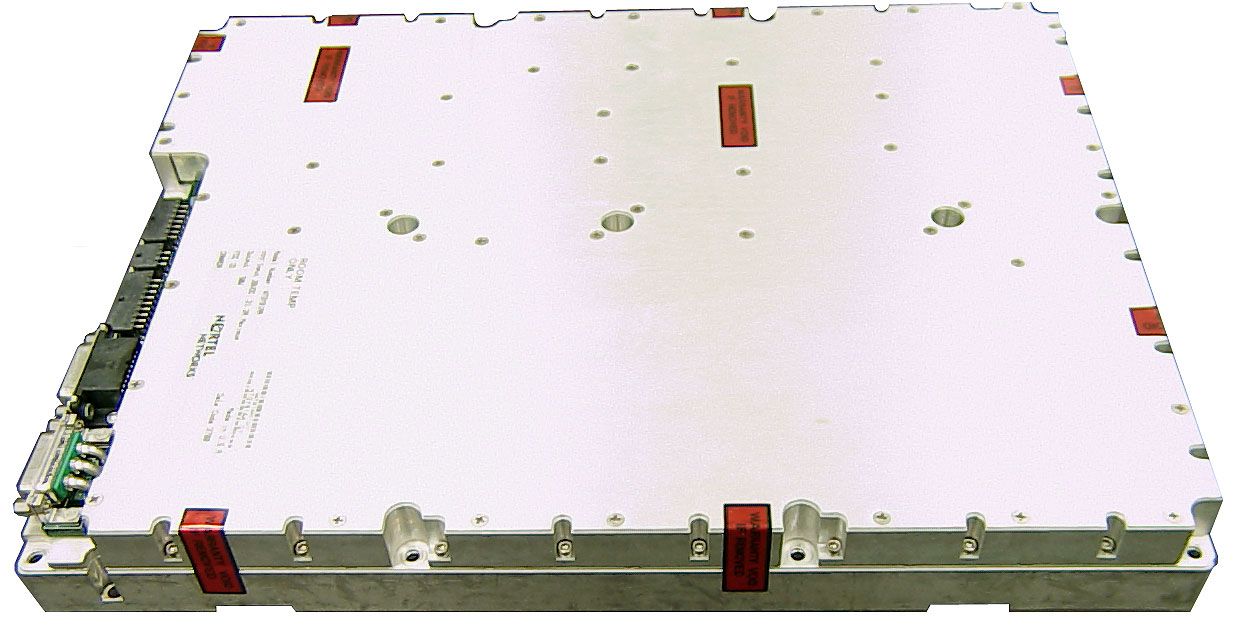
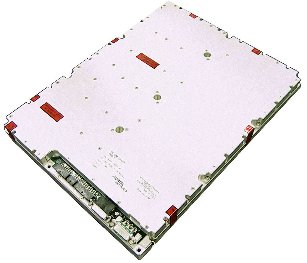
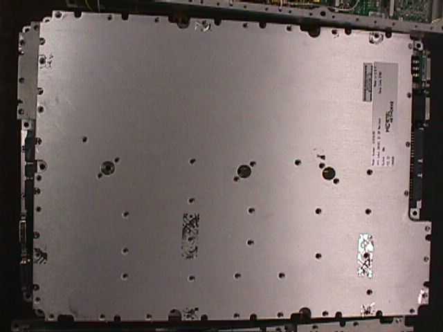
044-05079 Rev. A1-1 GENERAL DESCRIPTION 1-1. INTRODUCTION This manual contains information and procedures for installation, operation, and maintenance of Powerwave’s model NTGY81AA multichannel power amplifier (MCPA). The manual is organized into six sections as follows: Section 1. General Description Section 2. Installation Section 3. Operating Instructions Section 4. Principles of Operation Section 5. Maintenance Section 6: Troubleshooting 1-2. GENERAL DESCRIPTION The NTGY81AA is a linear, multichannel power amplifier that operates in the 60 MHz frequency band from 1930 MHz to 1990 MHz. It is designed to be mounted in an enclosure with EMI containment. Its flat base plate allows for mounting on a flat thermal-absorbing surface to provide adequate heat dissipation. Each amplifier module has a power, alarm, and control connector that allows the host system to monitor the amplifier module performance. Primary power for the amplifier is +26 Vdc. 1-3. FUNCTIONAL AND PHYSICAL SPECIFICATIONS Functional and physical specifications for the amplifier are listed in table 1-1. Section 1 044-05079 Rev. A1-2 Table 1-1. NTGY81AA Multichannel Power Amplifier Functional Specifications Frequency Range1930-1990 MHz (60 MHz Bandwidth) Maximum Average Input Power13 dBm Continuous Average Output Power50 Watts Spurious Emissions @ Maximum Rated Output Power (50 W / 47 dBm) Frequency OffsetRequirementMeas. Bandwidth Max.Min. 0.885-1.25 MHz-47 dBc30 kHz 1.25-1.98 MHz-16.5 dBm37.5 kHz 1.98-2.25 MHz-58 dBc30 kHz >2.25 MHz-15 dBm1 MHz RF Gain47 ±2 dB Gain Flatness:± 0.2 dB for any 1.25-MHz band within frequency range. Output Protection:Mismatch Protected Input Port Return Loss:VSWR 2:1 Max. Out of Band Spurious:Less than -15 dBm / 1 MHz DC Input Power:+26 ± 0.5 Vdc, 260 mV p-p max. ripple, ≤500 watts Operating Temperature:-15 ºC. to +85 ºC. (heatsink temperature) Storage Temperature:-40 ºC. to +85 ºC. Operating Humidity:5 % - 95 % Relative Humidity (Noncondensing) Storage Humidity:5 % - 95 % Relative Humidity (Noncondensing) Interface Connectors: RF Input--------------------------------------- RF Output------------------------------------- +26 Vdc Power and Ground------------ Alarms and Sensing---------------------- Differential IIC Clock, Rcv., Xmit.----- IIC, Power, Alarms, Controls----------- IIC, RS485, Power, Other Signals--- SMA Female SMA Female 3W3 D-Sub (Connector P1) 14-Position Micro-Fit 3.0 (Connector P2) 6-Position Micro-Fit 3.0 (Connector P3) 26-Position High Density D-Sub (Connector P4) 18-Position Micro-Fit 3.0 (Connector P5) Dimensions (inches):11.00 x 14.50; height: 1.70 044-05079 Rev. A1-3 P1 P4 P5 P3 P2 044-05079 Rev. A1-4 RF OUT RF IN Figure 1-1. NTGY81AA Multichannel Power Amplifier
Users Manual
044-05079 Rev. A2-1 INSTALLATION 2-1. INTRODUCTION This section contains unpacking, inspection, and installation instructions and recommendations for the Model NTGY81AA Single Channel Power Amplifier. Carefully read all material in this section prior to equipment unpacking or installation. Also read and review the operating procedures in Section 3 prior to installing the equipment. It is important that the licensee perform these tasks correctly and in good faith. If applicable, carefully read the appropriate parts of the Federal Communications Commission (FCC) rules to determine how they apply to your installation. DON'T TAKE CHANCES WITH YOUR LICENSE. 2-2. ELECTRICAL SERVICE RECOMMENDATIONS Powerwave Technologies recommends that proper AC line conditioning and surge suppression be provided on the primary AC input to the +26 Vdc power source. All electrical service should be installed in accordance with the National Electrical Code, any applicable state or local codes, and good engineering practice. Special consideration should be given to lightning protection of all systems in view of the vulnerability of most transmitter sites to lightning. Lightning arrestors are recommended in the service entrance. Straight, short ground runs are recommended. The electrical service must be well grounded. Each amplifier system should have its own circuit breaker, so a failure in one does not shut off the whole installation. Circuit breakers should be thermal type, capable of handling the maximum anticipated inrush current, in a load center with a master switch. 2-3. UNPACKING AND INSPECTION This equipment has been operated, tested and calibrated at the factory. Carefully open the container(s) and remove the amplifier module(s). Retain all packing material that can be reassembled in the event that the unit must be returned to the factory. CAUTION Exercise care in handling equipment during inspection to prevent damage caused by rough or careless handling. Visually inspect the amplifier module for damage that may have occurred during shipment. Check for evidence of water damage, bent or warped chassis, loose screws or nuts, or extraneous packing material in the connector. If the equipment is damaged, a claim should be filed with the carrier once the extent of any damage is assessed. We cannot stress too strongly the importance of IMMEDIATE careful inspection of the equipment and the subsequent IMMEDIATE filing of the necessary claims against the carrier if necessary. If possible, inspect the equipment in the presence of the delivery person. If the equipment is damaged, the carrier is your first area of recourse. If the equipment is damaged and must be returned to the factory, write or phone for a return authorization. Powerwave may not accept returns without a return authorization. Claims for loss or damage may not be withheld from any payment to Powerwave, nor may any payment due be withheld pending the outcome thereof. WE CANNOT GUARANTEE THE FREIGHT CARRIER'S PERFORMANCE Section 2 044-05079 Rev. A2-2 2-4. INSTALLATION INSTRUCTIONS (Refer to figure 1-1) The NTGY81AA amplifier module is designed for installation on a heatsink that permits access to the module for connection of RF cables and the power, alarm, and control connector. To install the amplifier proceed as follows: 1. Install amplifier on heatsink with thermally conductive material inserted between amplifier module and heatsink, and secure in place with appropriate mounting screws. 2. Connect the antenna cable to RF OUT female SMA connector. 3. Connect the transceiver output cable to RF IN frmale SMA connector. WARNING Turn off external primary DC power before connecting any cables. 4. Connect power, alarm, and control cables to matching P1 through P5 connectors. Refer to paragraphs 2-5 through 2-9 following. 6. Check your work before applying DC voltage to the system. Make certain all connections are tight and correct. 7. Measure primary DC input voltage. DC input voltage should be +26 ±0.5 Vdc. If the DC input voltage is above or below the limits, call and consult Powerwave before you turn on your amplifier system. 8. Refer to section 3 for initial turn-on and checkout procedures. 2-5. +26 VDC POWER AND GROUND CONNECTOR P1 The +26 Vdc power and ground connections on the amplifier are made through an 3-pin female D- Sub connector (figure 2-1) and are listed and described in table 2-1. 321 Figure 2-1. +26 Vdc Power and Ground Connector P1 Table 2-1. +26 Vdc Power and Ground Connector P1 Definition PINSIGNALDESCRIPTION 1+26V+26 Vdc for MCPA 2+26V_RTN+26 Vdc return, grounded to MCPA chassis ground. 3Chassis Gnd.Chassis Ground 044-05079 Rev. A2-3 044-05079 Rev. A2-4 2-6. ALARMS AND SENSING CONNECTOR P2 The alarms and sensing connections on the amplifier are made through a 14-pin micro-fit connector (figure 2-2) and are listed and described in table 2-2. Figure 2-2. Alarms and Sensing Connector P2 Table 2-2. Alarms and Sensing Connector P2 Definition PINSIGNALDESCRIPTION 1+5V_AIM5-volt supply for the AIM; routed directly to the fan assembly / AIM connector 2+5V_AIM_RTN5-volt supply return for the AIM; routed directly to the fan assembly / AIM connector 3+26V_ALARM26V HPCA alarm input 4+15V_ALARM15V HPCA alarm input 5REMOTE_SENSERemote sense for HPCA; connected directly to 26V supply 6REMOTE_SENSE_RTNRemote sense return for HPCA; connected directly to 26V supply return 7+5V_ALARM5V HPCA alarm input 8NCNot connected 926ARTN26V alarm return connected to 26V return on the MCPA 10ARTN5V and 15V alarm return connected to 26V return on the MCPA 11+26V_FAN26V supply for the fans; routed to fan assembly / AIM connector 12+26V_FAN_RTN26V supply return for the fans; routed to fan assembly / AIM connector 13+26V_FAN 26V supply for the fans; routed to fan assembly / AIM connector 14+26V_FAN_RTN26V supply return for the fans; routed to fan assembly / AIM connector 044-05079 Rev. A2-5 2-7. DIFFERENTIAL IIC CLOCK, RECEIVE, AND TRANSMIT CONNECTOR P3 The alarms and…
Text truncated - open the document above for the full version.
Users Manual
044-05079 Rev. A3-1 OPERATING INSTRUCTIONS 3-1. INTRODUCTION This section contains operating instructions for the Multicarrier Cellular Amplifier. 3-2. INITIAL START-UP AND OPERATING PROCEDURES There are no operating controls or indicators on the NTGY81AA amplifier module. To perform the initial start-up, proceed as follows: 1.Double check to ensure that all input and output cables are properly connected. CAUTION Before applying power, make sure that the input and output of the amplifier are properly terminated at 50 ohms. Do not operate the amplifier without a load attached. Refer to table 1-1 for input power requirements. Excessive input power may damage the amplifier NOTE The output coaxial cable between the amplifier and the antenna must be 50 ohm coaxial cable. Use of any other cable will distort the output. 2. Turn on supply that provides +26 Vdc to the amplifier system. 3.Turn on external exciter/transceiver and apply RF input signals. Section 3
Users Manual
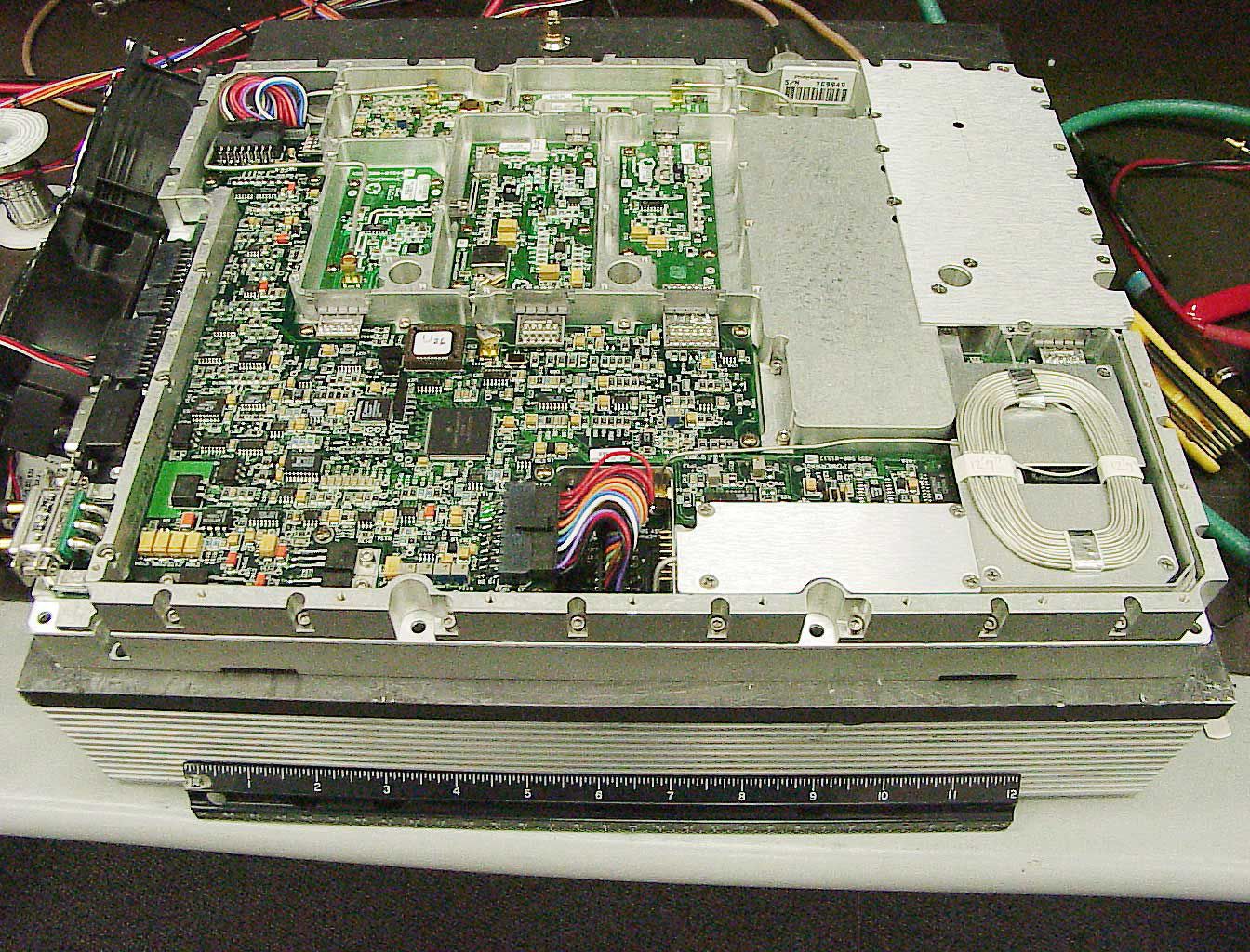
044-05079 Rev. A4-1 PRINCIPLES OF OPERATION 4-1. INTRODUCTION This section contains a functional description of the multichannel power amplifier (MCPA). 4-2. RF INPUT SIGNAL The maximum input power should not exceed the limits specified in table 1-1. 4-3. RF OUTPUT LOAD The load impedance should be as good as possible (1.5:1 or better) in the working band for good power transfer to the load. 4-4. AMPLIFIER FUNCTIONAL DESCRIPTION The NTGY81AA amplifier (figures 1-1 and 4-1) is a linear, multichannel power amplifier that operates in the 60 MHz frequency band from 1930 MHz to 1960 MHz at an output power of 50 watts. Each amplifier is a self-contained module and is functionally independent of any other amplifier modules in the system. Each amplifier module has an alarm board that monitors the amplifier performance. If a failure or fault occurs in an amplifier module, it is transmitted to the host system via an RS485 interface. The amplifier is compliant to the requirements of FCC Part 22 with respect to spurious emissions (see table 1-1). Constant gain is maintained by continuously comparing active paths with passive references, and correcting for small variations through the RF feedback controls. All gain variations, for example those due to temperature, are reduced to the passive reference variations. The amplifier module is comprised of: An input amplifier A predistortion amplifier A driver amplifier A main amplifier A multifunction board 4-4.1. INPUT AMPLIFIER RF is fed to the input amplifier, which consists of an isolator at the input, bandpass filter, VVAs, and phase shifters for gain control and phase sweeping functions. They are controlled by a microprocessor on the multifunction board. At its output, the input amplifier splits the signal to the predistortion amplifier and carrier cancellation circuits. 4-4.2. PREDISTORTION AMPLIFIER The predistortion amplifier predistorts the input signal in a way that it linearizes the output of the main amp at 50 watts. It also contains the main loop VVAs and phase shifters. All the predistortion voltages and loop voltages are controlled by a microprocessor. Section 4 044-05079 Rev. A4-2 4-4.3. DRIVER AMPLIFIER The driver amplifier consists of two stages of class AB amplification which provide approximately 40 dB of gain in the 60 MHz frequency band from 1930 MHz to 1990 MHz. The amplifier operates on +26 Vdc, and a safe bias voltage which is controlled by microprocessors. 4-4.4. MAIN AMPLIFIER The main amplifier employs two class AB amplification stages for maximum efficiency. It provides approximately 25 dB of gain in the 60 MHz frequency band. The output from the main amplifier is typically 48.6 dBm. The amplifier operates on +26 Vdc, and gate bias voltages controlled by microprocessors. 4-4.5. MULTIFUNCTION BOARD The multifunction board consists of control and alarm circuits. The MCPA communicates to the host system through the multifunction board which gathers the status information of the amplifier and reports to the host system via the RS485 interface when instructed. It also protects the MCPA from adverse conditions such as overpower, input overdrive, overvoltage, etc. A microprocessor on the multifunction board also controls two loops in the feed-forward system. 4-5. AMPLIFIER MODULE COOLING Each amplifier module is contained within a thermally conductive chassis which, when properly mounted on an adequate thermal surface, will provide sufficient cooling to maintain the amplifier within the specified operating temperature range. 4-6. POWER DISTRIBUTION Primary DC power for the amplifier is provided by the host system. The amplifier generates all the required voltages internally from the main source. RF IN INPUT AMPLIFIER PREDISTORTION AMPLIFIER DRIVER AMPLIFIER MAIN AMPLIFIER RF OUT MULTIFUNCTION BOARD (ALARMS AND LOOP CONTROLS) Figure 4-1. NTGY81AA Multichannel Power Amplifier Functional Block Diagram
Users Manual
044-05079 Rev. A5-1 MAINTENANCE 5-1. INTRODUCTION This section contains periodic maintenance and performance test procedures for the multichannel power amplifier. It also contains a list of test equipment required to perform the identified tasks. NOTE Check your sales order and equipment warranty before attempting to service or repair the unit. Do not break the seals on equipment under warranty or the warranty will be null and void. Do not return equipment for warranty or repair service until proper shipping instructions are received from the factory. 5-2. PERIODIC MAINTENANCE Periodic maintenance requirements are listed in Table 5-1. Table 5-1 also lists the intervals at which the tasks should be performed. Table 5-1. Periodic Maintenance TASKINTERVALACTION Inspection Cables and Connectors12 MonthsInspect signal and power cables for frayed insulation. Check RF connectors to be sure that they are tight. Performance Tests12 MonthsPerform annual test per paragraph 5-5. 5-3. TEST EQUIPMENT REQUIRED FOR TEST Test equipment required to test the amplifier is listed in Table 5-2. Equivalent test equipment may be substituted for any item, keeping in mind that a thermistor type power meter is required. NOTE All RF test equipment must be calibrated to 0.05 dB resolution. Any deviation from the nominal attenuation must be accounted for and factored into all output readings. Section 5 044-05079 Rev. A5-2 Table 5-2. Test Equipment Required MENCLATUREMANUFACTURERMODEL Signal GeneratorAgilent (H.P.)ESG4433B 30 dB Attenuator, 250 WattTenuline Spectrum AnalyzerH.P.8562E Coax Directional CouplerH.P.778D Power Meter / SensorH.P.437B / 8481A Network AnalyzerH.P.8753D Current Probe Source DiskettePowerwave Driver PA (1930-1990 MHz)12 dB gain, P 1dB = 29 dBm (min) 5-4. PERFORMANCE TEST Performance testing should be conducted every 12 months to ensure that the amplifier system meets the operational specifications listed in table 5-3. Also verify system performance after any amplifier module is replaced in the field. The test equipment required to perform the testing is listed in table 5-2, and the test setup is shown in figure 5-1. 5-4.1. AMPLIFIER PERFORMANCE TEST. To perform the test, proceed as follows: 1.Connect test equipment as shown in figure 5-1. NOTE Do not apply any RF signals at this time. AMPLIFIER SPURIOUS EMISSIONS TEST: 2.Load the MFRM waveform on the ESG (signal generator). Apply this signal through a driver amplifier to the MCPA so that the RF signal going into the MCPA is approximately 0 dBm (adjust the input RF signal level to get 47 dBm output power). Measure spurious emissions. Verify that it is within specification. GAIN TEST: 3.Set input power level to power amplifier at 0 dBm (1932, 1960, and 1987 MHz). 4. Measure the output power in dBm. 5. Subtract input power (in dBm) from output power (in dBm) to get gain. 6.Check the amplifier gain across the band from 1930 MHz to 1990 MHz. Gain should be 47 ±2 dB. Record test data in table 5-3. INPUT RETURN LOSS TEST: 7.Read and record the S 11 return loss measurement on network analyzer. Record test data in table 5-3. 044-05079 Rev. A5-3 Figure 5-1. NTGY81AA Amplifier Test Setup Diagram 044-05079 Rev. A5-4 Table 5-3. Multichannel Power Amplifier NTGY81AA Test Data Sheet Tested By: ___________________Serial No: ________________ Pass/Fail: ____________________Date: ____________________ 50W MCPA Test Test Conditions: Load and source impedance: 50 ohms, VSWR < 1.2:1 Supply voltage: +26 Vdc ±± 0.4 Vdc (unless otherwise noted). Network Analyzer Span: 60 MHz Marker #1 = 1930 MHz, #2 = 1960 MHz, #3 = 1990 MHz TEST CONDITIONMINMAXFREQUENCY (MHz) 1.00NETWORK ANALYZER193019601990 1.01Gain45.0 dB49.0 dB 1.02Gain Flatness0 dB0.4 dB/ 1.25 MHz 1.03Input Return Loss, worst case In band-10 dB 1.04Output Return Loss, worst case in band-15 dB 2.00CDMA TESTS (Spurious Emissions) 3 TONE: W-CDMA @ 50W out RBW= 3KHz; VBW=10KHz 2.01? @ +2.25 Mhz-16 dBm/ 1 MHz 2.02? @ –2.25 Mhz-16 dBm/ 1 MHz 2.032 nd Harmonic 386039203980 -16 dBm/ 1 MHz 2.04Pilot 192519451965 16 dBm/ 1 MHz 2.05Current @ 50 W out19 A 044-05079 Rev. A5-5 5-5. FIELD REPLACEMENT OF THE MODULE The NTGY81AA multichannel power amplifier module can be replaced in the field on site by a qualified technician with experience maintaining RF power amplifiers and similar equipment. To replace a power amplifier module, proceed as follows: 1. Turn off 26 Vdc power to that specific module. 2. Disconnect the two RF cables and connectors P1 through P5. 3. Remove 13 screws that secure amplifier module to heat sink. 4. Carefully remove amplifier module from heat sink. 5. Add Thermstrate thermal interface pad to surface of replacement amplifier which mates with heatsink. 6. Install replacement in reverse order of steps 1 through 4 above.
Users Manual
044-05079 Rev. A6-1 TROUBLESHOOTING 6-1INTRODUCTION This section contains a list of problems which users have encountered and a few suggested actions that may correct the problem. If the suggested corrective action does not eliminate the problem, please contact your Powerwave field representative or the factory for further instructions. NOTE Check your sales order and equipment warranty before attempting to service or repair the unit. Do not break the seals on equipment under warranty or the warranty will be null and void. Do not return equipment for warranty or repair service until proper shipping instructions are received from the factory. 6-2TROUBLESHOOTING Refer to table 6-1 for troubleshooting suggestions. Table 6-1. Troubleshooting. SYMPTOMSUGGESTED ACTION MCPA Inoperative1.Check for proper power supply voltage. MCPA Not Enabled1.Verify HPA-Allow-Enable line is high. Alarm Output is (RS 422) HighVerify input RF is within specified power and frequency limits 6-3RETURN FOR SERVICE PROCEDURES When returning products to Powerwave, the following procedures will ensure optimum response. 6-3.1Obtaining an RMA A Return Material Authorization (RMA) number must be obtained prior to returning equipment to the factory for service. Please contact our Repair Department at (949) 809-1100 to obtain this number, or FAX your request to (949) 757-6676. Failure to obtain this RMA number may result in delays in receiving repair service. 6-3.2Repackaging for Shipment To ensure safe shipment of the amplifier, it is recommended that the package designed for the amplifier be used. The original packaging material is reusable. If it is not available, contact Powerwave’s Customer Service Department for packing materials and information. Section 6
Attestation Statements
Report No. 0383-08 (FCC ID: E675JS0046) Page 1 Rev.No 1.0 ATTESTATION STATEMENT SUMMARY: All tests according FCC Part 2, Paragraphs 2.1046, 2.1051, 2.1053, and Part 42, Paragraph 24.238 were ! - Performed The Equipment Under Test ! - Fulfills FCC Part 2, Paragraphs 2.1046, 2.1051, 2.1053, and Part 42, Paragraph 24.238 requirements. - TÜV PRODUCT SERVICE, INC. - Responsible Engineer: Jim Owen (EMC Engineer)
Block Diagram
RF IN INPUT AMPLIFIER PREDISTORTION AMPLIFIER DRIVER AMPLIFIER MAIN AMPLIFIER RF OUT MULTIFUNCTION BOARD (ALARMS AND LOOP CONTROLS) Figure 4-1. NTGY81AA Multichannel Power Amplifier Functional Block Diagram
ID Label/Location Info
From: Jeff Dale <[email protected]>, on 10/25/00 8:51 AM: Hi Mary, The labels go on the top cover of the amplifier module.
Operational Description
044-05079 Rev. A4-1 PRINCIPLES OF OPERATION 4-1. INTRODUCTION This section contains a functional description of the multichannel power amplifier (MCPA). 4-2. RF INPUT SIGNAL The maximum input power should not exceed the limits specified in table 1-1. 4-3. RF OUTPUT LOAD The load impedance should be as good as possible (1.5:1 or better) in the working band for good power transfer to the load. 4-4. AMPLIFIER FUNCTIONAL DESCRIPTION The NTGY81AA amplifier (figures 1-1 and 4-1) is a linear, multichannel power amplifier that operates in the 60 MHz frequency band from 1930 MHz to 1960 MHz at an output power of 50 watts. Each amplifier is a self-contained module and is functionally independent of any other amplifier modules in the system. Each amplifier module has an alarm board that monitors the amplifier performance. If a failure or fault occurs in an amplifier module, it is transmitted to the host system via an RS485 interface. The amplifier is compliant to the requirements of FCC Part 22 with respect to spurious emissions (see table 1-1). Constant gain is maintained by continuously comparing active paths with passive references, and correcting for small variations through the RF feedback controls. All gain variations, for example those due to temperature, are reduced to the passive reference variations. The amplifier module is comprised of: An input amplifier A predistortion amplifier A driver amplifier A main amplifier A multifunction board 4-4.1. INPUT AMPLIFIER RF is fed to the input amplifier, which consists of an isolator at the input, bandpass filter, VVAs, and phase shifters for gain control and phase sweeping functions. They are controlled by a microprocessor on the multifunction board. At its output, the input amplifier splits the signal to the predistortion amplifier and carrier cancellation circuits. 4-4.2. PREDISTORTION AMPLIFIER The predistortion amplifier predistorts the input signal in a way that it linearizes the output of the main amp at 50 watts. It also contains the main loop VVAs and phase shifters. All the predistortion voltages and loop voltages are controlled by a microprocessor. Section 4 044-05079 Rev. A4-2 4-4.3. DRIVER AMPLIFIER The driver amplifier consists of two stages of class AB amplification which provide approximately 40 dB of gain in the 60 MHz frequency band from 1930 MHz to 1990 MHz. The amplifier operates on +26 Vdc, and a safe bias voltage which is controlled by microprocessors. 4-4.4. MAIN AMPLIFIER The main amplifier employs two class AB amplification stages for maximum efficiency. It provides approximately 25 dB of gain in the 60 MHz frequency band. The output from the main amplifier is typically 48.6 dBm. The amplifier operates on +26 Vdc, and gate bias voltages controlled by microprocessors. 4-4.5. MULTIFUNCTION BOARD The multifunction board consists o…
Text truncated - open the document above for the full version.
Contact Information
Applicant
Jeff Dale(Principal Reliability Engineer)
Test Firm
TUV AmericaJames Owen
Technical Specifications
| # | Rule Parts | Frequency Range | Power Output | Emission |
|---|---|---|---|---|
| 1 | 24 | 1.93 GHz - 1.99 GHz | 50 W | F9W |
Other Applications from Powerwave Technologies Inc
E675JS0123
Nov 03, 2011Multi-carrier RF Power Amplifier
Equipment Class
AMP - Amplifier
E675JS0120
Aug 26, 2010Nexus Dual Band Repeater
Equipment Class
TNB - Licensed Non-Broadcast Station Transmitter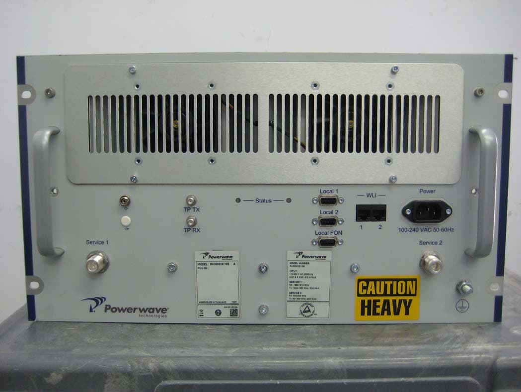
E675JS0119
Aug 01, 2010Nexus Dual Band Repeater
Equipment Class
PCB - PCS Licensed Transmitter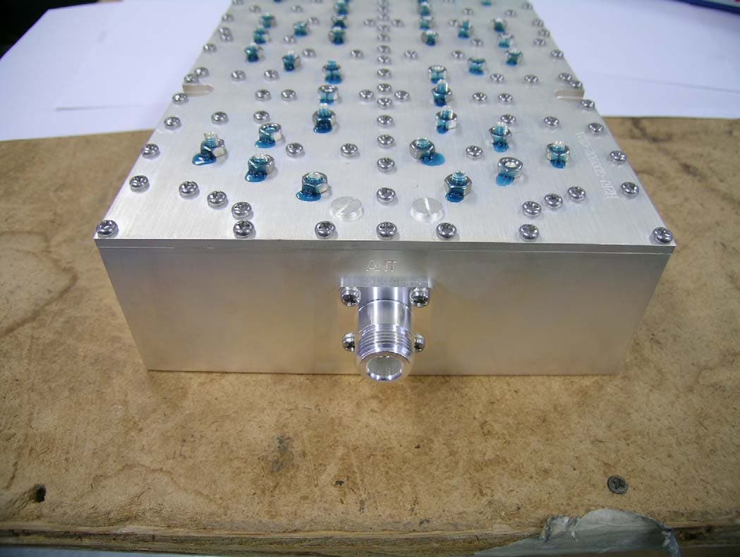
E675JS0118
Jul 26, 2010Nexus Dual Band Repeater
Equipment Class
PCB - PCS Licensed Transmitter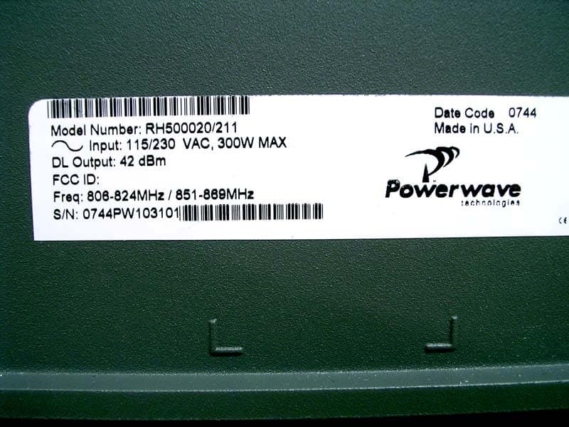
E675JS0096
Jan 10, 2008Wideband Radio Head
Equipment Class
TNB - Licensed Non-Broadcast Station Transmitter