E675JS0050G3L-800-60-004
Powerwave Technologies Inc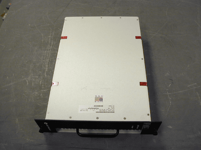
Click to zoom
Application Details
- Equipment Class
- AMP - Amplifier
- Date of Grant
- Dec 14, 2000
- Application Purpose
- Original Equipment
- Date of Application
- Dec 14, 2000
- Equipment Note
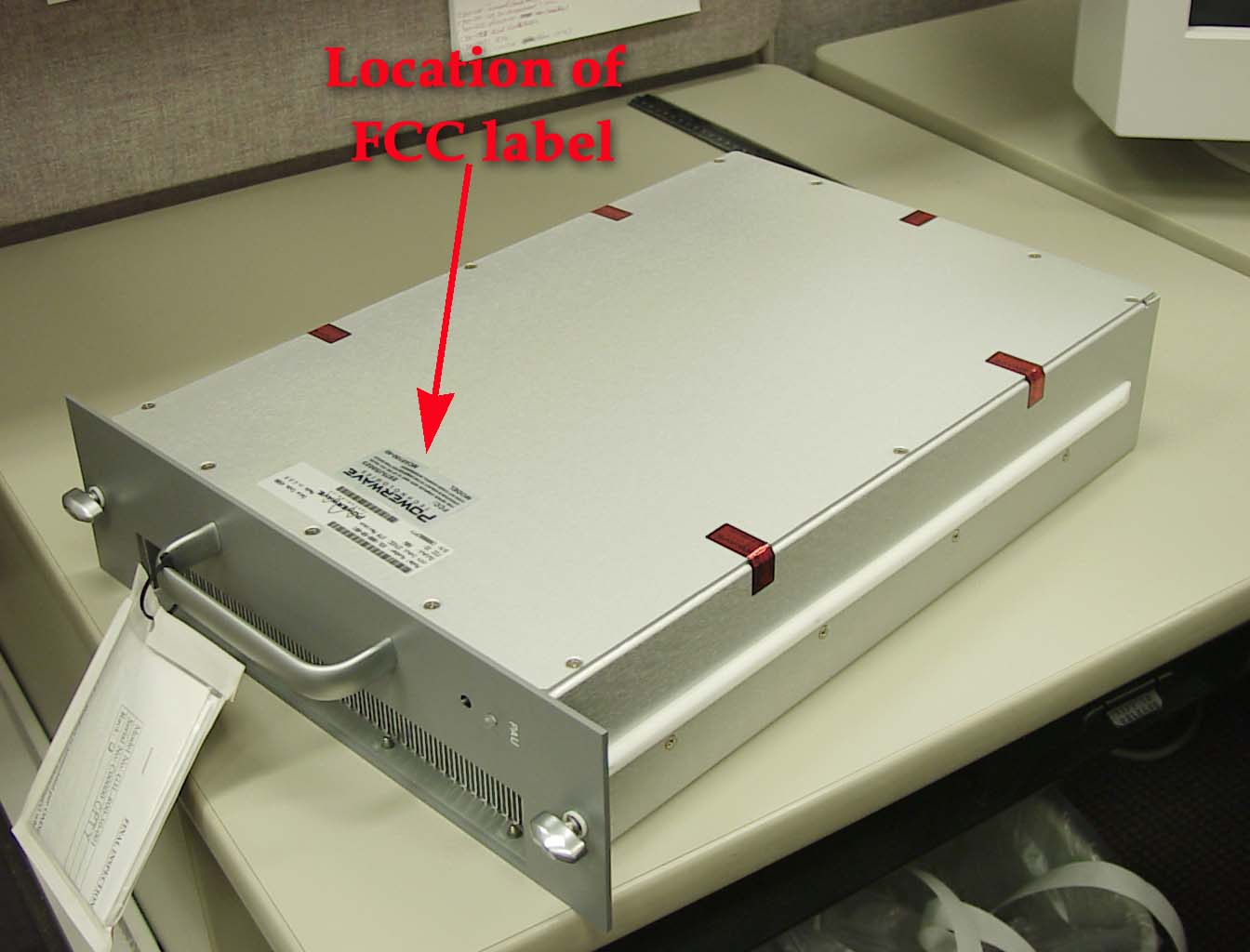
- G3L-800-60-004
- Frequency Range
- 869.00000000 - 894.00000000
- Company
- Powerwave Technologies Inc
- Country
- United States
Documents & Files

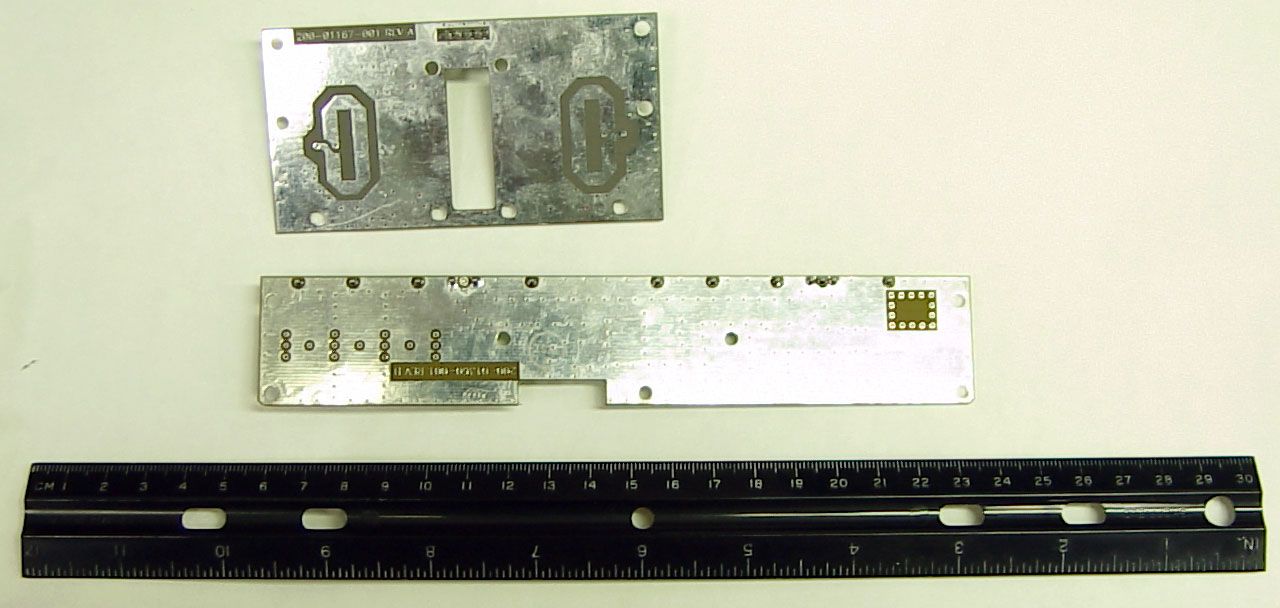
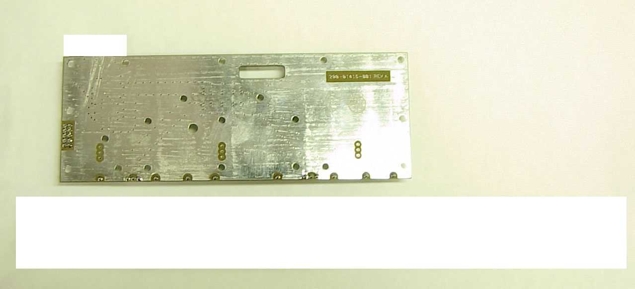
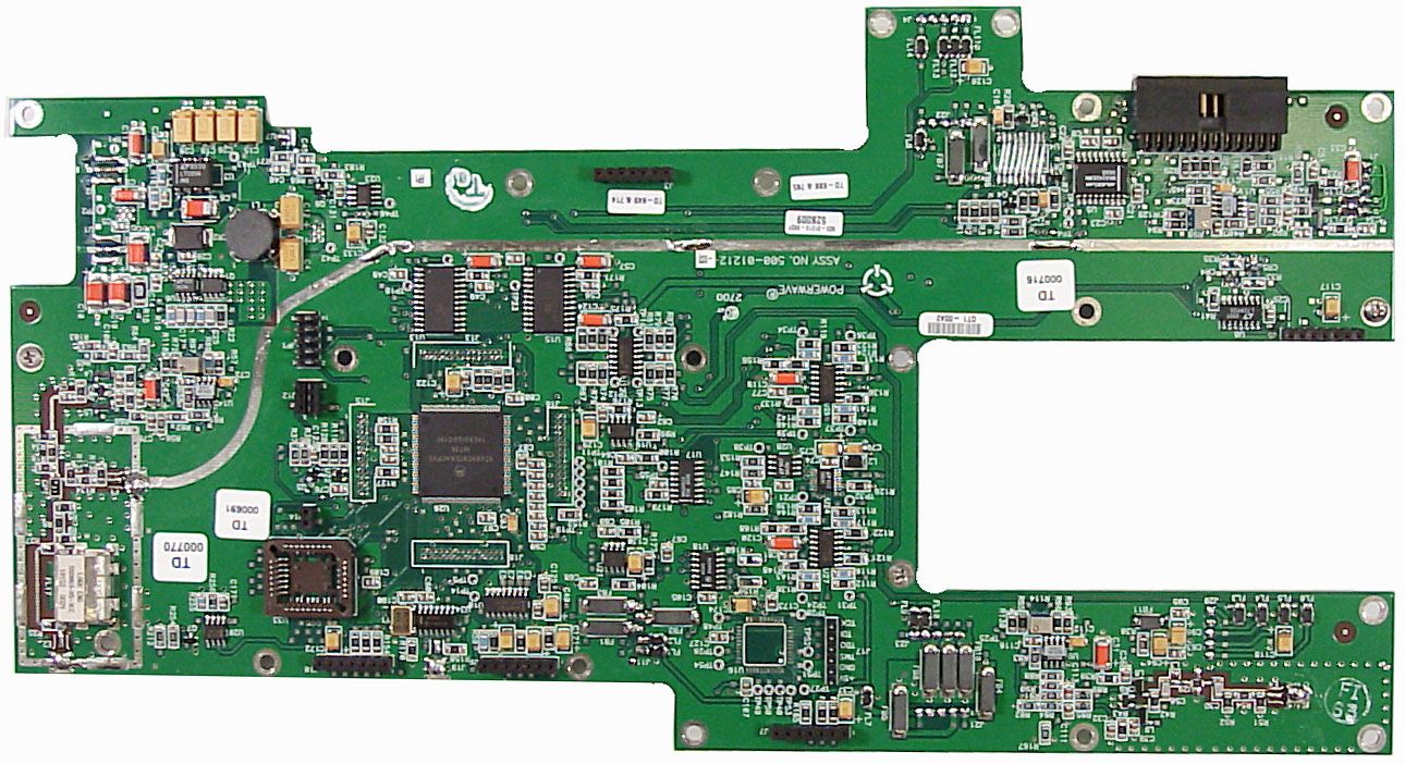
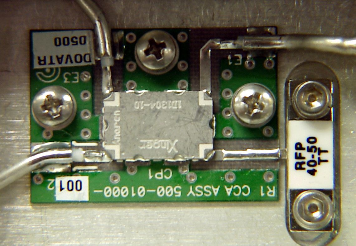
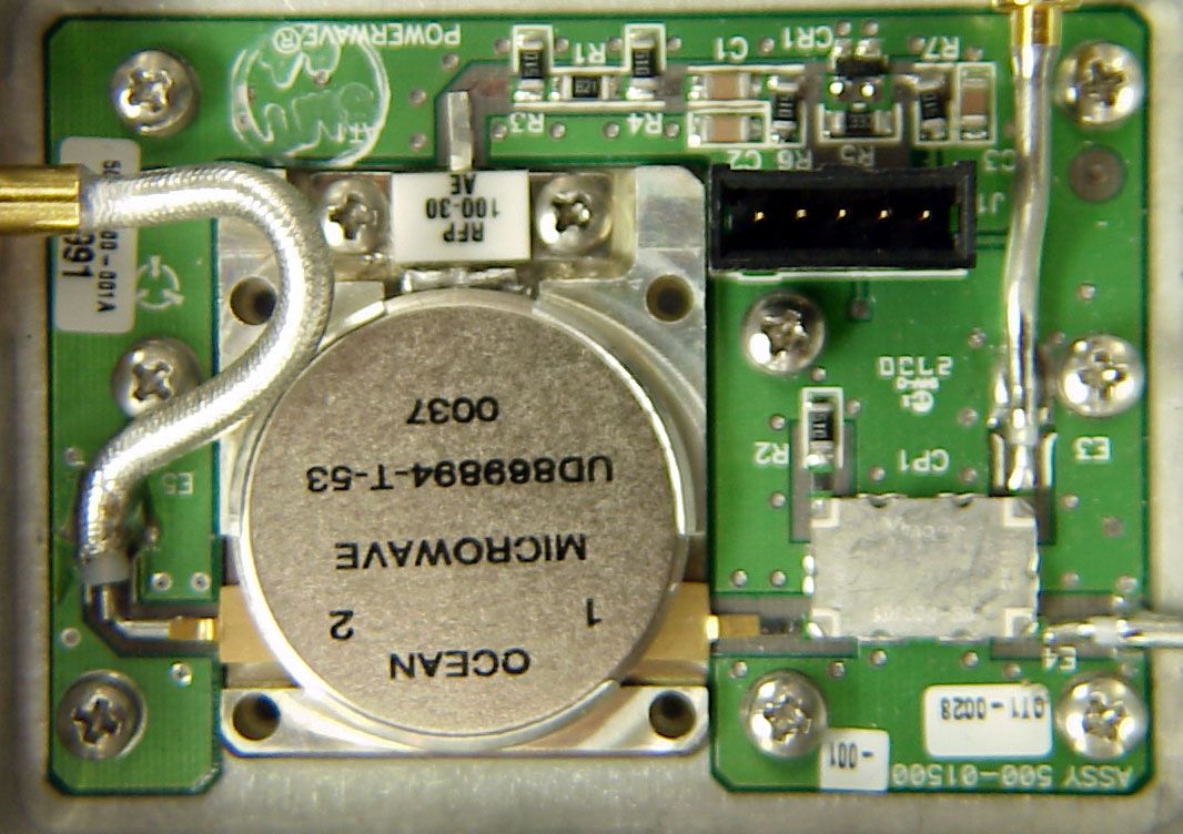
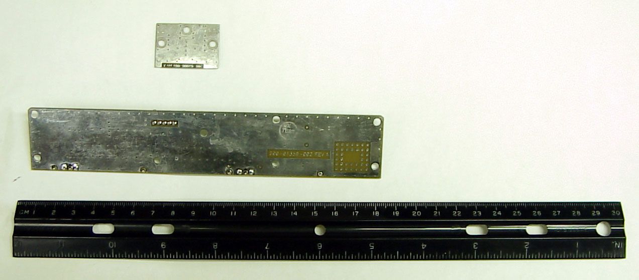
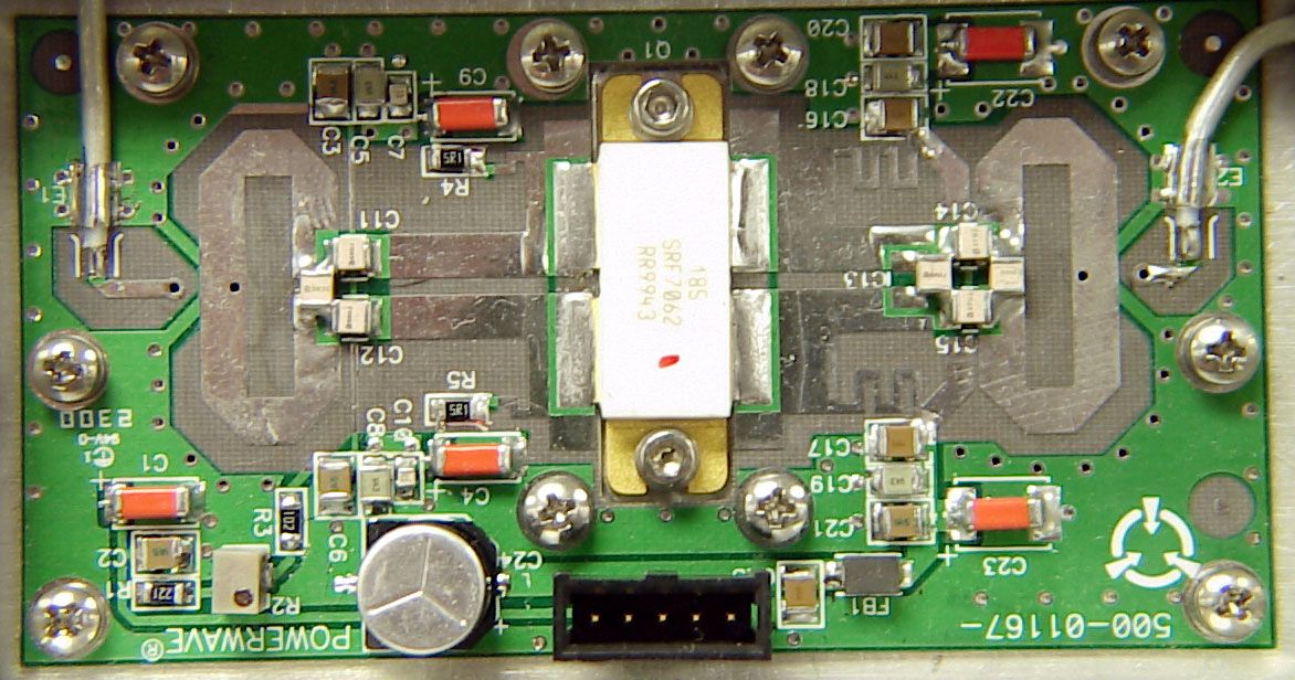
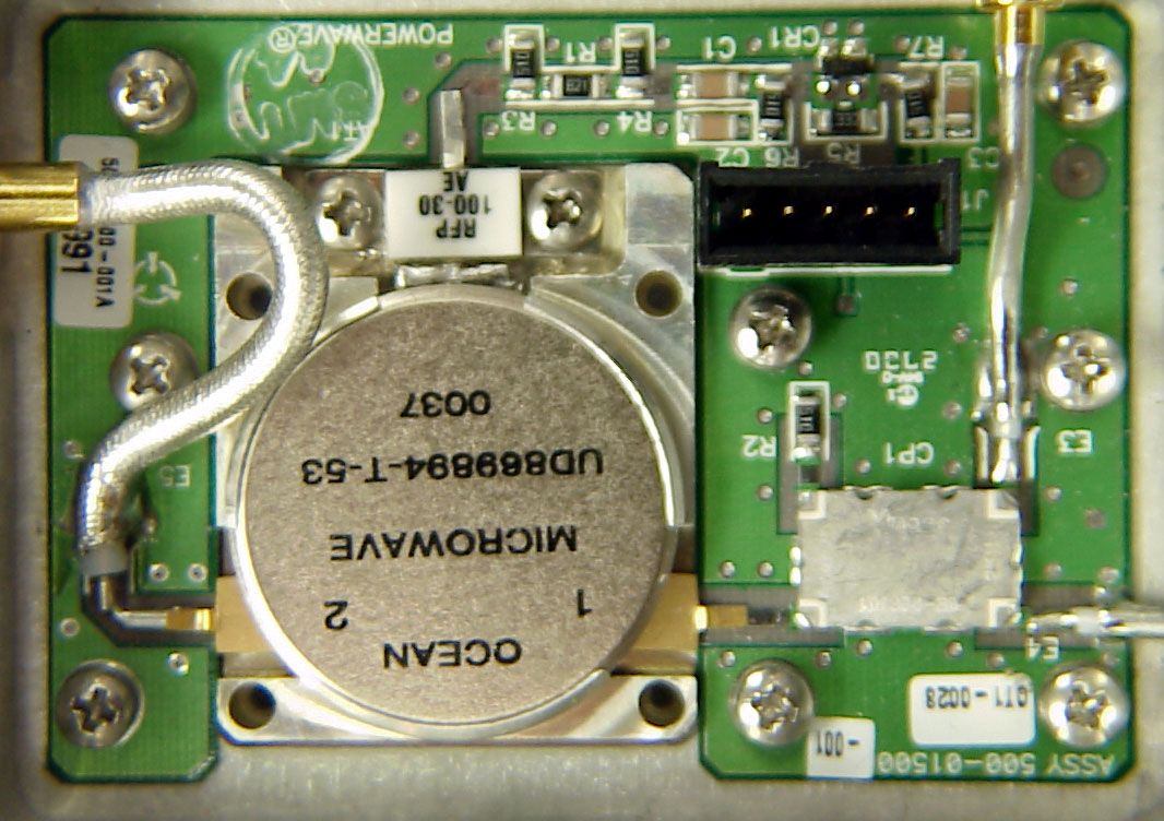
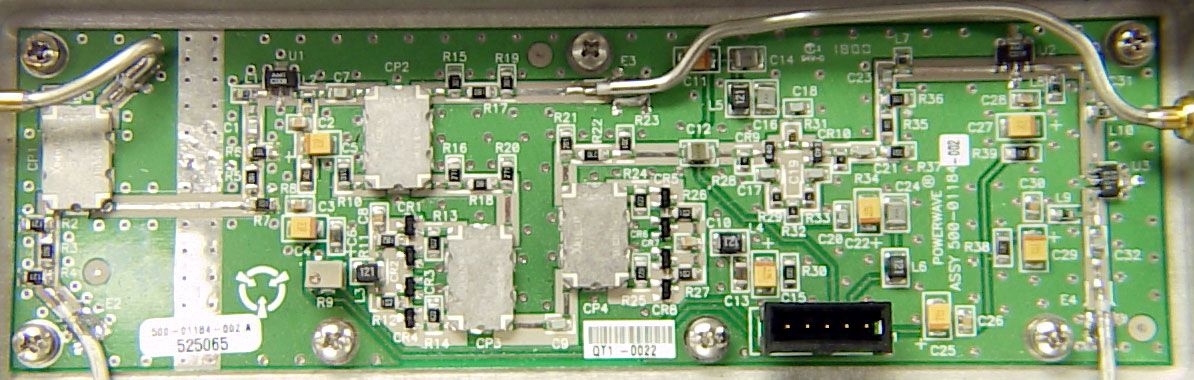
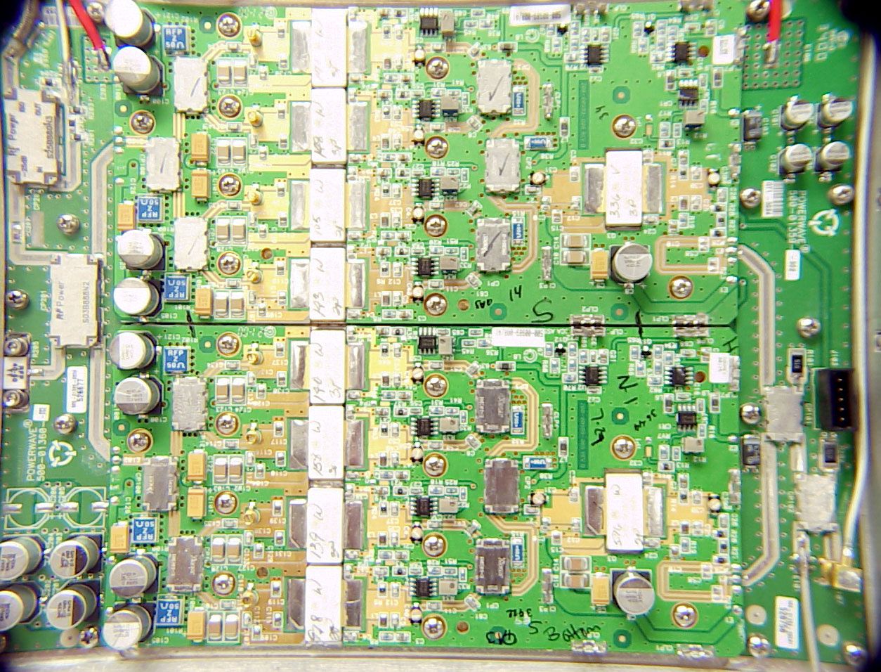
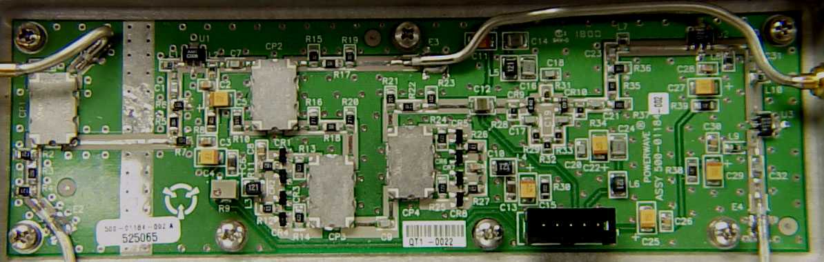
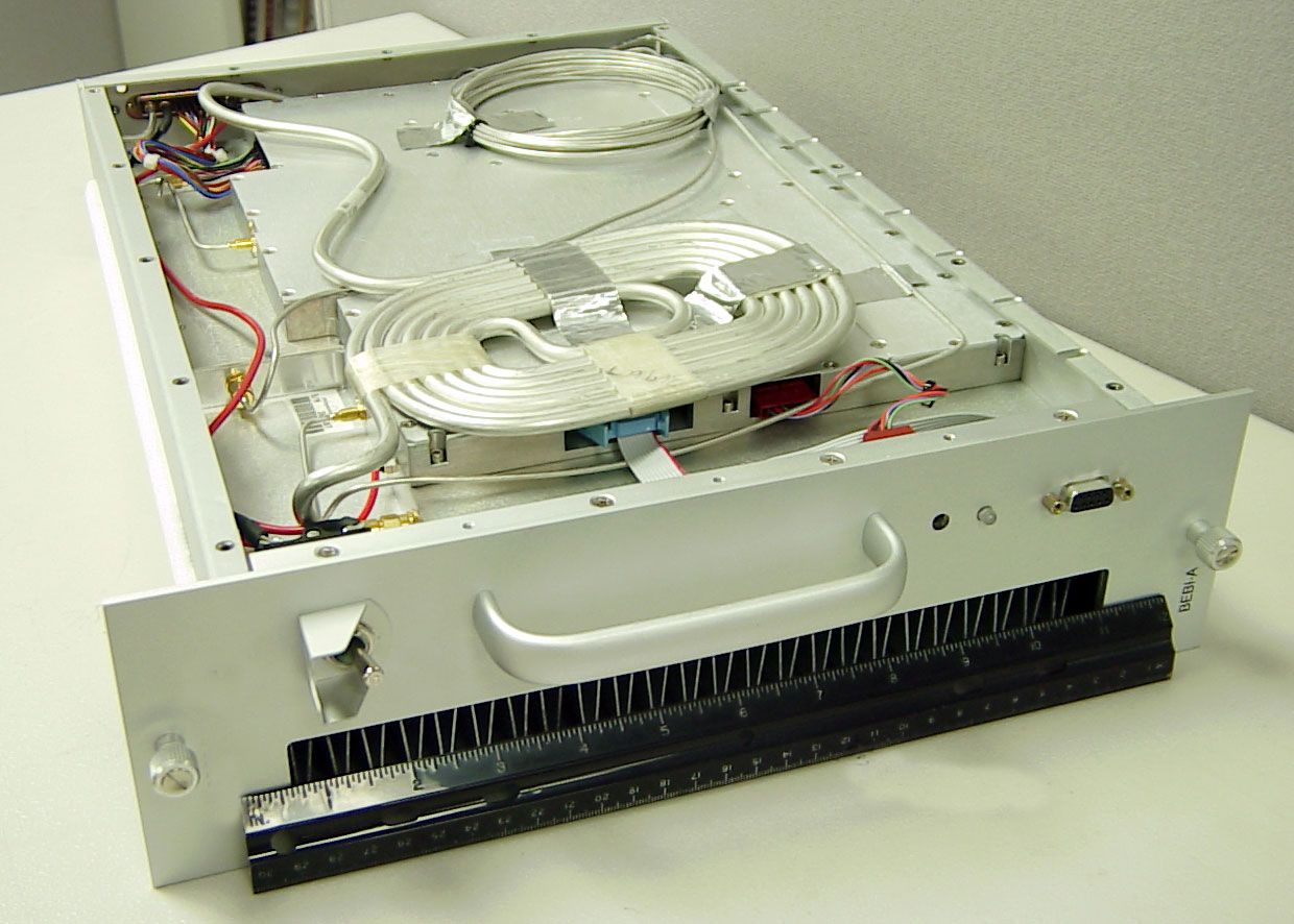
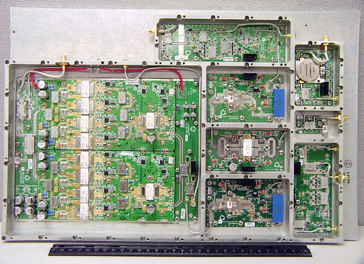
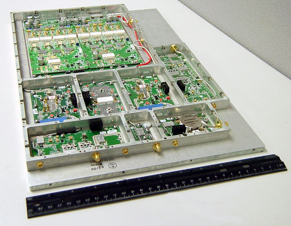
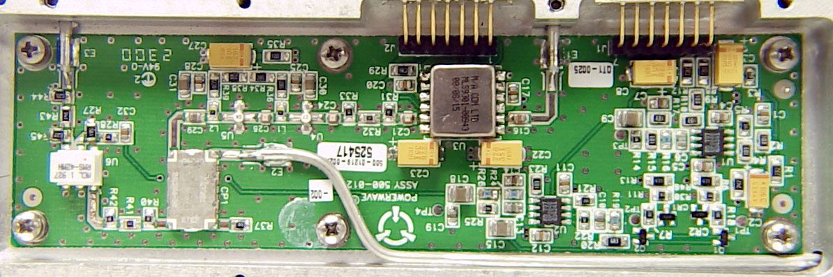
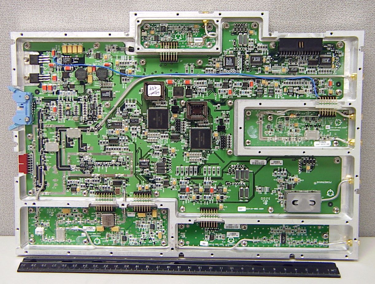
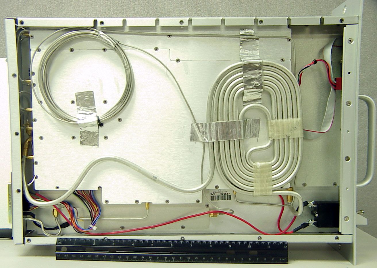
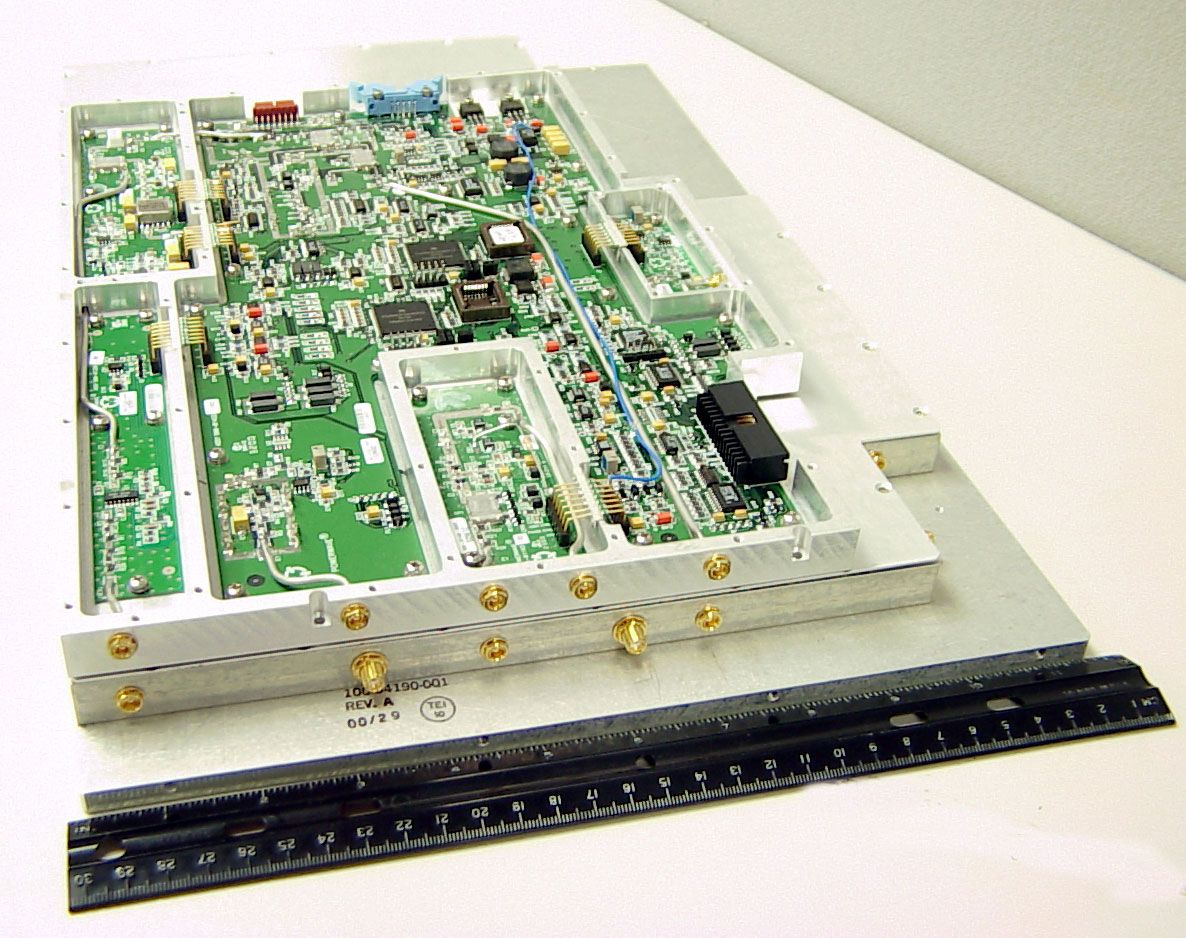
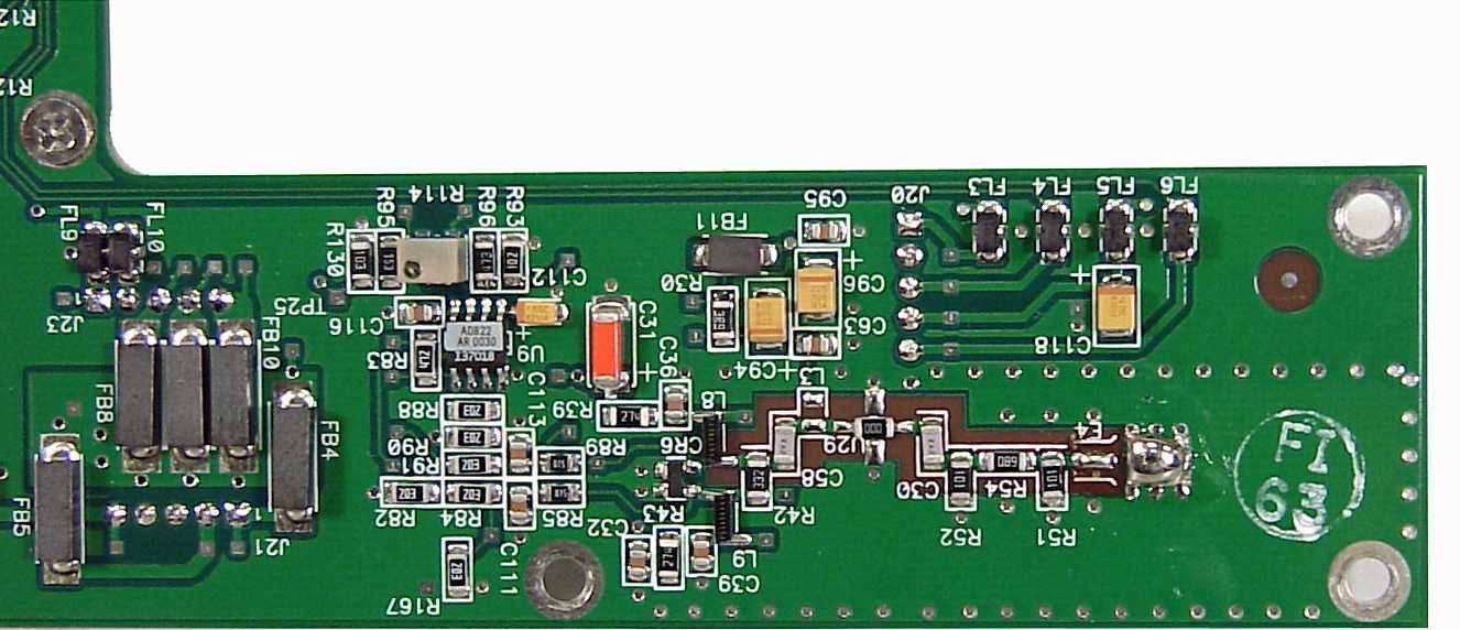
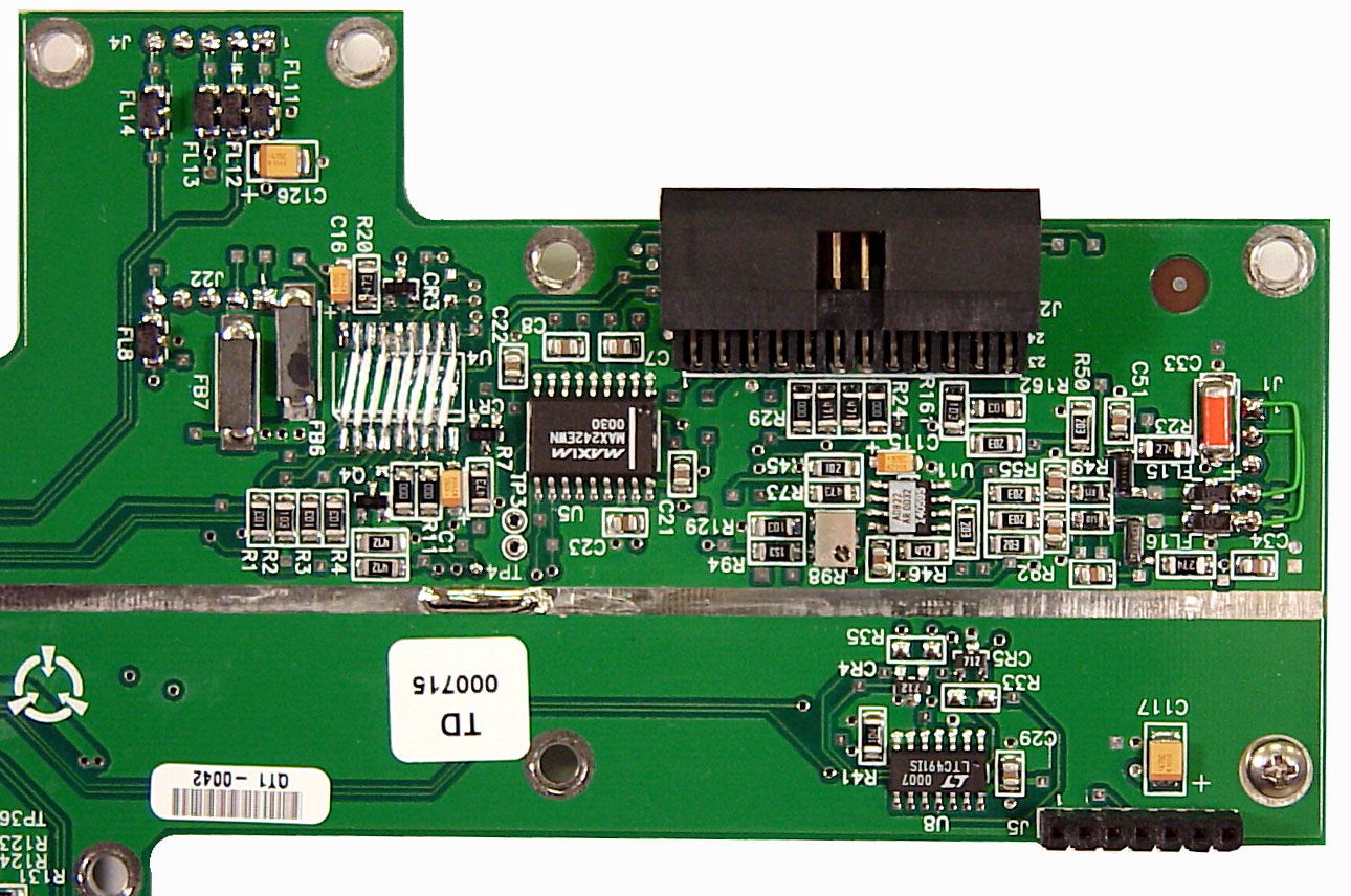
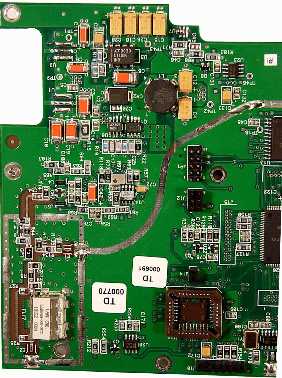
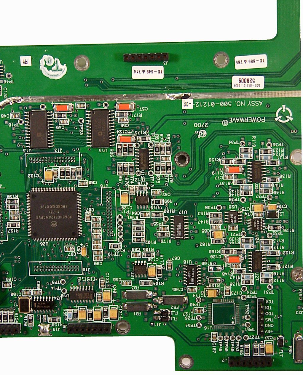
Document Text
Text extracted from the exhibit documents filed with the FCC. Open a document above to read the original.
Users Manual
Booster Amplifier Subrack System Integration Manual 044-05075 Rev. A System Integration Manual Booster Amplifier Subrack (BAS) System 869-894 MHz, 91 Watts Maximum Booster Amplifier Subrack System Intergration Manual 044-05078 Rev. Aii November 2000 Powerwave Technologies, Inc.Tel: (949) 809-1100 2026 McGaw AvenueFax: (949) 757-0941 Irvine, CA 92614Web Site: www.powerwave.com © 2000 Powerwave Technologies Incorporated. All rights reserved. Powerwave Technologies, and the Powerwave logo are registered trademarks Powerwave Technologies, Inc. reserves the right to make changes to the documentation and equipment, including but not limited to component substitution and circuitry changes. Changes that impact this manual may subsequently be incorporated in a later revision of this manual. ® 044-05078 Rev. A iii Table Of Contents Par.Section 1Page No.General DescriptionNo. 1-1Introduction.................................................................................................. 1-1 1-2General Description ..................................................................................... 1-1 1-3Functional And Physical Specifications .......................................................... 1-2 1-3.1 MCR20830-1 Subrack Specifications............................................................. 1-3 1-3.2 G3L-800 Series Amplifier Specifications......................................................... 1-5 1-4Booster Amplifier Subrack Major Components ............................................... 1-8 1-5Equipment Changes...................................................................................... 1-8 Section 2 Installation 2-1Introduction.................................................................................................. 2-1 2-2Site Survey ................................................................................................... 2-1 2-3Electrical Service Recommendations .............................................................. 2-1 2-4 Air Conditioning............................................................................................ 2-1 2-5Unpacking and Inspection............................................................................. 2-2 2-6Installation Instructions ................................................................................ 2-3 2-7Amplifier Module Power, Alarm, Control, and RF Connector ........................... 2-4 2-8Remote Control and Status ........................................................................... 2-5 Section 3 Operating Instructions 3-1Introduction.................................................................................................. 3-1 3-2Initial Start-Up and Operating Procedures ..................................................... 3-1 Section 4 Principles of Operation 4-1Introduction.................................................................................................. 4-1 4-2RF Input Signal............................................................................................. 4-1 4-3RF Output Load ............................................................................................ 4-1 4-4System Functional Description ...................................................................... 4-1 4-5Multi-Carrier Power Amplfier Functional Description ..................................... 4-2 4-5.1 Predriver Amplifier ........................................................................................ 4-3 4-5.2 Three Stage Driver Amplifier.......................................................................... 4-3 4-5.3 Main Amplifier .............................................................................................. 4-3 4-5.4 Alarm Monitoring and Control ....................................................................... 4-3 4-5.5 Loop Control Circuit...................................................................................... 4-3 4-6Amplifier Module Cooling............................................................................... 4-4 4-7Power Distribution ........................................................................................ 4-4 044-05078 Rev. A iv Table Of Contents (Continued) Par.Section 5Page No.MaintenanceNo. 5-1Introduction.................................................................................................. 5-1 5-2Periodic Maintenance .................................................................................... 5-1 5-3Test Equipment Required For Test................................................................. 5-1 5-4Performance Test .......................................................................................... 5-2 5-4.1 Amplifier Performance Test............................................................................ 5-2 5-4.1.1 Amplifier Spurious Emissions Test ................................................................ 5-2 5-4.1.2 Gain Test ...................................................................................................... 5-2 5-4.1.3 Input Return Loss ......................................................................................... 5-2 5-5Field Replacement of the Module ................................................................... 5-5 Section 6 Troubleshooting 6-1Introduction.................................................................................................. 6-1 6-2Troubleshooting ............................................................................................ 6-1 6-3Return for Service Procedures ....................................................................... 6-1 6-3.1 Obtaining an RMA......................................................................................... 6-1 6-3.2 Repackaging for Shipment............................................................................. 6-1 List Of Appendices Page AppendixNo. ABooster Amplifier Subrack Backplane Wiring Diagram .............…
Text truncated - open the document above for the full version.
Attestation Statements
Report No. 0467-08 (FCC ID:E675JS0050) Page 1 Rev.No 1.0 ATTESTATION STATEMENT All tests according FCC Part 2, Paragraphs, 2.1046, 2.1047, 2.1051, 2. 1053 and Part 22, Paragraph 22.917(e) were. n - Performed The Equipment Under Test n - Fulfills the requirements of FCC Part 2, Paragraphs, 2.1046, 2.1047, 2.1051, 2. 1053 and Part 22, Paragraph 22.917(e). - TÜV PRODUCT SERVICE, INC. - Responsible Engineer: Jim Owen (EMC Engineer)
Block Diagram
MCR 20830-1 MCR 20830-1 60w 60w RS-485 Alarm Interface VVA C o m b i n e r GAIN CTRL Splitter Distribution Circuit Board (DC,Fans, Alarms) ISO ISO -25dB Sample DB9 Alarm Alarm Ctrl 2x +27VDC 2x Ground RF Input 869-894 MHz RF Output GL3-800-60 30 dB System Block Diagram Pre Amp Pre Main Main Amp Error Amp Delay Feed Forward Loop control 2nd Loop Phase & Gain 1st Loop Phase & Gain Delay Alarms & Display +15 +5 -5 Power Supply -30dB -10dB -40dB RF Out RFL PWR FWD PWR Front Panel Smart Rack +27VDC Multi-Carrier Power Amplifier Functional Block Diagram
Operational Description
Booster Amplifier Subrack System Integration Manual 044-05078 Rev. A 4-1 November 2000 Section 4. Principles of Operation 4-1 Introduction This section contains a functional description of Powerwave Technologies Inc.’s, Booster Amplifier Subrack (BAS) system. Refer to Figure 4-1 for the system’s functional block diagram. 4-2 RF Input Signal The maximum input power for all carrier frequencies to the system should not exceed the limits specified in Section 1, Table 1-2. 4-3 RF Output Load The load impedance should be as good as possible (VSWR of 1.5:1 or better) in the working band for good power transfer to the load. If the amplifier is operated into a filter, it will maintain its dis- tortion characteristics outside the signal band even if the VSWR is infinite, provided the reflected power does not exceed one Watt. A parasitic signal of less than one-Watt incident on the output will not cause distortion at a higher level than the normal forward distortion (i.e. –65 dBc). MCR 20830-1 MCR 20830-1 60w 60w RS-485 Alarm Interface VVA C o m b i n e r GAIN CTRL Splitter Distribution Circuit Board (DC,Fans, Alarms) ISO ISO -25dB Sample DB9 Alarm Alarm Ctrl 2x +27VDC 2x Ground RF In put RF Output GL3-800-60 30 dB Figure 4-1 System Block Diagram 4-4 System Functional Discription Designed as a subrack for installation in a 2-way transceiver paging base station, the BAS system is comprised of a MCR20830-1 Booster Amplifier Subrack (BAS) and two G3L-900-60 plug-in multi-carrier power amplifiers (MPCAs). Additionally, the BAS houses a two-way power splitter/combiner and a distribution printed circuit board (PCB). Refer to Appendix A for pinout locations. The RF IN, RF OUT, +27 Vdc and the ALARM summary connector, interface with the host system via front panel cabling. The RF input signal is split equally and applied to the plug-in amplifiers. The output from each am- plifier is an amplified composite signal of approximately 60 Watts before combiner losses. All phase and gain corrections are performed on the signal(s) in the individual amplifier. The amplifier Booster Amplifier Subrack System Integration Manual 044-05078 Rev. A 4-2 November 2000 outputs are fed to a power combiner and combined to form a composite RF output of up to 91 Watts after combiner losses. Refer to Figure 4-1 for the System Functional Block Diagram. The distribution printed circuit board (PCB) assembly is used to distribute power to the BAS sys- tem’s internal components. The PCB circuit is a DC/DC converter designed to convert the +27 Vdc input to +12 Vdc and +15 Vdc. Refer to Appendix B for pinout location. 4-5 Multi-Carrier Power Amplifier (MCPA) Functional Description The MCPA is a linear, feed-forward multi-carrier power amplifier that operates in the 5 MHz fre- quency band from 869 MHz to 894 MHz at an output power 60 Watts. Each amplifier is a self- contained module and is functionally independent of the other MCPA in the system. The amplifiers are designed for parallel operation to achieve high peak power output (refer to Table 1-2 for MPCA power specifications). Each MCPA has an alarm board that monitors the amplifier per- formance. If a failure or fault occurs in an MCPA, it is transmitted to the host system via the D- subminiature 21WA4 connector at the rear of the module. A warning light (LED), which is routed from the amplifier via the J7 connector on the PCB to the front panel of the BAS, will illuminate. The indicator LEDs are identified as Alarm 1 and Alarm 2 which corresponds to their respective amplifier.. The amplifier is compliant to the requirements of FCC Part 22 with respect to spurious emissions. Constant gain is maintained by continuously comparing active paths with passive references, and correcting for small variations through the RF feedback controls. All gain variations, for example those due to temperature, are reduced to the passive reference variations. The amplifier is com- prised of: A preamp A driver amplifier A main amplifier An error and pre-error amplifier Alarm monitoring and control Pre Amp Pre Main Main Amp Error Amp Delay Feed Forward Loop control 2nd Loop Phase & Gain 1st Loop Phase & Gain Delay Alarms & Display +15 +5 -5 Power Supply -30dB -10dB -40dB RF Out RFL PWR FWD PWR Front Panel Smart Rack +27VDC Figure 4-2 Multi-Carrier Power Amplifier Functional Block Diagram Booster Amplifier Subrack System Integration Manual 044-05078 Rev. A 4-3 November 2000 4-5.1 Pre-driver Amplifier The input of the amplifier uses two stages of class AB amplification which provide approximately 13.5 dB of gain in the 5 MHz frequency band from 869 MHz to 894 MHz. The amplifier operates on +27 Vdc. 4-5.2 Three-Stage Driver Amplifier The input of the amplifier uses three stages of class AB amplification which provide approximately 32 dB of gain in the 5 MHz frequency band from 869 MHz to 894 MHz. The amplifier operates on +27 Vdc, and a bias voltage of +5 Vdc. The logic controls the +5 Vdc bias voltage that shuts down the amplifier. 4-5.3 Main Amplifier The signal provides approximately 11 dB of gain in the 869 to 894 MHz frequency band. The out- put from the main amplifier is typically 60 Watts. The main amplifier operates on +27 Vdc, and a bias voltage of +5 Vdc. The alarm logic controls the +5 Vdc bias voltage that shuts down the am- plifier. The main amplifier employs class AB amplification for maximum efficiency. The error amplifier and feed forward loops are used to correct signal non linearities introduced by the class AB main am- plifier. The error amplifier operates in class A mode. The RF input signals are amplified by a pre- amp and coupled to an attenuator and phase shifter in the first feed-forward loop. The main signal is phase shifted by 180 degrees and amplified in the premain amplifier. The output from the pre- main amplifier is fed to the class AB main amplifier. The signal output from the main amplifier is sampled using a coupler, and the sample signal is combined with the main input…
Text truncated - open the document above for the full version.
Parts List/Tune Up Info
Booster Amplifier Subrack System Integration Manual 044-05078 Rev. A5-1November 2000 5-1 Test Equipment Required For Test Test equipment required to test the amplifier is listed in Table 5-2. Equivalent test equipment may be substituted for any item, keeping in mind that a thermistor type power meter is required. NOTE All RF test equipment required must be calibrated to 0.05 dB resolution. Any deviation from the nominal attenuation must be accounted for and factored into all output readings. Table 5-2. Test Equipment Required NomenclatureManufacturerModel Signal GeneratorH.P.8656B 20 dB Attenuator, 250 WattBirdTenuline 20 dB Attenuator, 20 Watt (2 each)BirdTenuline Spectrum AnalyzerH.P.8560E Coax Directional CouplerH.P.778D Power Meter / SensorH.P.437B / 8481A Arbitrary Waveform GeneratorSonyAWG2021 Network AnalyzerH.P.8753C Source DiskettePowerwave 5-2 Performance Test Performance testing should be conducted every 12 months to ensure that the amplifier system meets the operational specifications listed in Table 5-3. Also verify system performance after any amplifier module is replaced in the field. The test equipment required to perform the testing is listed in Table 5-2, and the test setup is shown in Figure 5-1. NOTE The frequencies used in this test are typical for an amplifier with a 5 MHz band from 869 MHz to 894 MHz. Select evenly spaced F1, F2, F3, and F4 frequencies that cover the instantaneous bandwidth of your system. 5-2.1 Amplifier Performance Test To perform this test, proceed as follows: Connect test equipment as shown in Figure 5-1. WARNING Do not apply any RF signals at this time. 5-2.1.1 Amplifier Spurious Emissions Test: With the RF input signal to the amplifier set to be as shown in Figure 5-1, use the spectrum ana- lyzer to measure the spurious emissions performance. Record test data in Table 5-3. Verify that it is within the specifications shown in Table 1-2. Switch tested amplifier to OFF. Booster Amplifier Subrack System Integration Manual 044-05078 Rev. A5-2November 2000 5-2.1.2 Gain Test: 1. Disconnect spectrum analyzer from test setup, and connect the network analyzer. 2. Set network analyzer as follows: A. Power output to -13 dBm. B. Frequency start to 869 MHz. C. Frequency stop to 894 MHz. D. Normalize the network analyzer for gain and return loss. 3. Check the amplifier gain across the band from 869 MHz to 894 MHz. Gain should be as specified in Table 1-2. Record test data in Table 5-3. 5-2.1.3 Input Return Loss: Read and record the S 11 return loss measurement on network analyzer. Record test data in Table 5- 3. Figure 5-1 Amplifier Test Setup Diagram Booster Amplifier Subrack System Integration Manual 044-05078 Rev. A5-3November 2000 Table 5-3. Multi-Carrier Power Amplifier Test Data Sheet DATE____________________________________ MODULE S/N_____________________________ TEST CONDITIONS: Load and Source Impedance: 50 Ohms VSWR: < 1.2:1 Supply Voltage: +27 Vdc ±0.1 Vdc TESTSPECIFICATIONMINMAXDATA RF GainVcc = 27 Vdc PO = 50 W Freq. = 869 – 894 MHz Table 1-2 - 0.5 dB Table 1-2 +0.5 dB Spurious Emissions Vcc = 27 Vdc PO =50 W 869 - 894 MHz Band -65 dBc Gain FlatnessVcc = 27 Vdc PO =50 W 869 - 894 MHz Band ±0.5 dB Input Return Loss Vcc = 27 Vdc PO = 50 W 869 - 894 MHz Band -12 dB PASS FAIL Tested by Booster Amplifier Subrack System Integration Manual 044-05078 Rev. A5-4November 2000 5-3 Field Replacement of the Module The GL3-900-60 multi-carrier power amplifier module can be replaced in the field on site by a quali- fied technician with experience maintaining RF power amplifiers and similar equipment: To replace a power amplifier module, proceed as follows: 1. Set on/off switch on the front panel of the amplifier module to OFF (down). 2. Loosen two thumbscrews that secure amplifier module to subrack. CAUTION When removing the amplifier from the subrack, it is very important to support the amplifier such that the rear of the module does not suddenly drop when the guide rail disengages from the track. A drop such as this could damage the rear 21WA4 multipin connector. 3. With steady even pressure, use handle on front of amplifier to pull module out of subrack. 4. Install replacement in reverse order of steps 1 through 3 above.
RF Exposure Info
FCC Equipment Authorization Application Exhibit Type of Exhibit:Statement Concerning RF Exposure FCC Rule Part:47 CFR 1.1307 Manufacturer:Powerwave Technologies Model:Seahawk FCC ID(s):E675JS0050 Date:12/06/00 Per the FCC Rules and Regulations as described in OET Bulletin 65, this device is categorically excluded from routine evaluation because these are used at fixed installations with antennas mounted on outdoor, permanent structures and fall well below the power limits requiring RF evaluation in accordance with 47 CFR 1.1307.
Test Report
Report No. 0467-08 (FCC ID:E675JS0050) Page 1 Rev.No 1.0 MEASUREMENT AND TECHNICAL REPORT POWERWAVE TECHNOLOGIES 2026 McGaw Avenue Irvine, CA 92614 DATE: 08 December 2000 This Report Concerns:Original Grant: XClass II Change: Equipment Type:Seahawk 800, Model G3L-800-60 Deferred grant requested per 47 CFR 0.457(d)(1)(ii)?Yes: Defer until: No: X Company Name agrees to notify the Commission by:N/A of the intended date of announcement of the product so that the grant can be issued on that date. Transition Rules Request per 15.37?Yes:*No: (*) FCC Part 2, Paragraphs, 2.1046, 2.1047, 2.1051, 2. 1053 and Part 22, Paragraph 22.917(e) Report Prepared by: TÜV PRODUCT SERVICE 10040 Mesa Rim Road San Diego, CA 92121-2912 Phone: 858 546 3999 Fax: 858 546 0364 Report No. 0467-08 (FCC ID:E675JS0050) Page 2 Rev.No 1.0 TABLE OF CONTENTS Pages 1 GENERAL INFORMATION3 1.1Product Description3 1.2Related Submittal Grant6 1.3Tested System Details6 1.4Test Methodology6 1.5Test Facility6 1.6Part 2 Requirements6 2 SYSTEM TEST CONFIGURATION7 2.1Justification7 2.2EUT Exercise Software7 2.3Special Accessories7 2.4Equipment Modifications7 2.5Configuration of Tested System7 3RADIATED EMISSION EQUIPMENT/DATA8 Field Strength Calculation12 4 CONDUCTED EMISSION EQUIPMENT/DATA13 5Signature page28 Report No. 0467-08 (FCC ID:E675JS0050) Page 3 Rev.No 1.0 1 GENERAL INFORMATION 1.1Product Description EUT Description Multi-channel power amplifier EUT Name G3L-800-60 Model No.: G3L-800-60Serial No.: -- Product Options: N/A Configurations to be tested: 60 Watt output Power Requirements Voltage: 27 Vdc (If battery powered, make sure battery life is sufficient to complete testing.) # of Phases: N/A Current (Amps/phase(max)): 30A Current (Amps/phase(nominal)): N/A Other Typical Installation and/or Operating Environment (ie. Hospital, Small Business, Industrial/Factory, etc.) Telcom Report No. 0467-08 (FCC ID:E675JS0050) Page 4 Rev.No 1.0 1.1Product Description (continued) EUT Power Cable PermanentORRemovableLength (in meters): ShieldedORUnshielded Not Applicable EUT Interface Ports and Cables InterfaceShielding TypeTypeTermination Connector TypePort Termination RF/In/Out DC Power Metalized D- Sub RF connections/dc power EUT Operating Modes to be Tested -- 1. RF applied to reach 60 watt output EUT System Components -- DescriptionModel #Serial #FCC ID # Power amplifier module G3L-800-60 Support Equipment DescriptionModel #Serial #FCC ID # HP Signal Generator E4436B US39260103 HP Power MeterE4419BGB40201926 RF Cables & Connectors Oscillator Frequencies Frequency Derived FrequencyComponent # / LocationDescription of Use 15 MHz 15 MHzY1 Multifunction BoardClock Power Supply ManufacturerModel #Serial #Type N/A Switched-mode:(Frequency) Report No. 0467-08 (FCC ID:E675JS0050) Page 5 Rev.No 1.0 1.1Product Description (continued) Power Line Filters ManufacturerModel #Location in EUT Spectrum Control52-978-107-FA3 Multifunction Board PanasonicELK-E103FAMultifunction Board Critical EMI Components (Capacitors, ferrites, etc.) DescriptionManufacturerPart # or ValueQtyComponent # / Location Ferrite Fair-Rite 274302144710 FB1-FB10 Multifunction Bd Bandpass FilterPanasonicELK-E103FA FL17/Multifunction Bd EMC Critical Detail -- Describe other EMC Design details used to reduce high frequency noise. Inductive filters, capacitive filters, noise filters Report No. 0467-08 (FCC ID:E675JS0050) Page 6 Rev.No 1.0 1 GENERAL INFORMATION (continued) 1.2Related Submittal/Grant None 1.3Tested System Details The FCC IDs for all equipment, plus descriptions of all cables used in the tested system are: None 1.4Test Methodology Purpose of Test:To demonstrate compliance with the ANSI C63.4 setup. Test Performed:X1. Conducted Emissions, FCC Part 2, Paragraphs 2.1047, 2.1051 and Part 22, Paragraph 22.917(e) 2. Radiated Emissions EN55022: 1992 Class B limit, 30 - 1,000 MHz, 10 meters X3. Radiated Emission per FCC Part 2, Paragraph 2.153 4. Engineering evaluations 5. Frequency Stability, Part 2, Paragraph 2.995, and Part 87, Paragraph 87.133 XRF Output Power, Part 2, Paragraph 1.1046 Both Conducted and radiated testing were performed according to the procedures in FCC/ANSI C63.4 and CSA 108.8 - M1983. Radiated testing was performed at an antenna-to-EUT distance of 3 meters (1 - 10 GHz). 1.5Test Facility The open area test site and conducted measurement data were tested by: TÜV PRODUCT SERVICE 10040 Mesa Rim Road San Diego, CA 92121-2912 Phone: 619 546 3999 Fax: 619 546 0364 The Test Site Data and performance comply with ANSI 63.4 and are registered with the FCC, 7435 Oakland Mills Rd, Columbia Maryland 21046. All Measurement Data is acquired according to the content of FCC Measurement Procedure and ANSI C63.4, unless supplemented with additional requirements as noted in the test report. 1.6 Part 2 Requirements Multi-channel power amplifier. Microprocessor Model Number: MC68HC812A4 DC voltages applied to and dc currents into the several elements of the final radio frequency amplifying device for normal operation over the power range. 27 Vdc / 30 A Equipment does not employ digital modulation techniques. Report No. 0467-08 (FCC ID:E675JS0050) Page 7 Rev.No 1.0 2.SYSTEM TEST CONFIGURATION 2.1Justification The Seahawk was initially tested for FCC emission in the following configuration: See Block Diagram. 2.2EUT Exercise Software None 2.3Special Accessories None 2.4Modification None 2.5Configuration of Tested System See Block Diagram. Report No. 0467-08 (FCC ID:E675JS0050) Page 8 Rev.No 1.0 3RADIATED EMISSION EQUIPMENT/DATA The following data lists the significant emission frequencies, measured levels, correction factor (which includes cable and antenna corrections), the corrected reading, and the limit. See following page(s). See test setup photos for radiated emissions test setup. Report No. 0467-08 (FCC ID:E675JS0050) Page 11 Rev.No 1.0 Emissions Test Conditions: RADIATED EMISSIONS, FCC Part 2, Paragraph 2.1053 The RADIATED EMISSIONS measurements were performed at the foll…
Text truncated - open the document above for the full version.
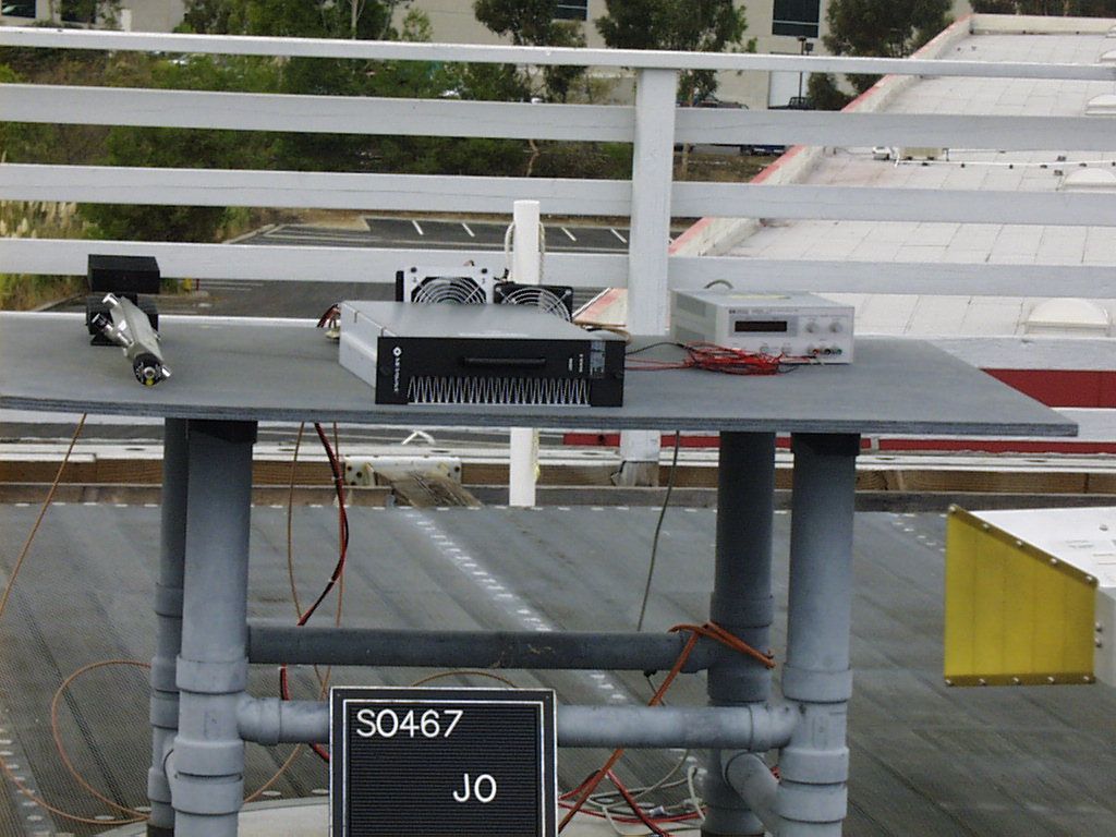
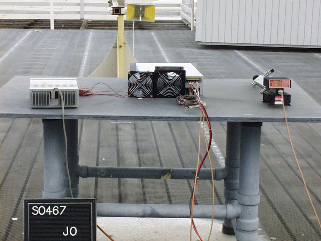
Test Setup Photos
General Test Setup SG#1 SG#2 SG#3 Combiner EUT IN OUT AT1 AT2DC1 PS1 PM1SA
Contact Information
Applicant
Jeff Dale(Principal Reliability Engineer)
Test Firm
TUV AmericaJames Owen
Technical Specifications
| # | Rule Parts | Frequency Range | Power Output | Emission |
|---|---|---|---|---|
| 1 | 22.901(d) | 869 MHz - 894 MHz | 60 W | F9W |
Other Applications from Powerwave Technologies Inc
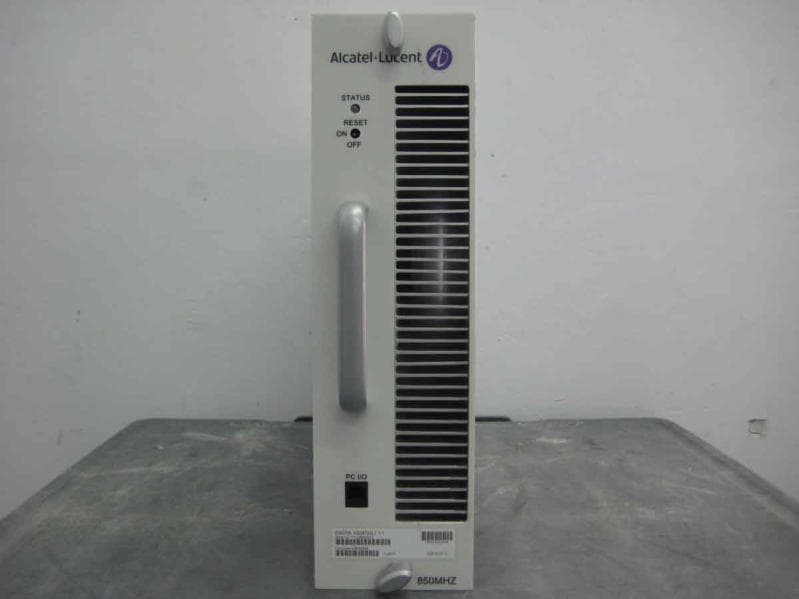
E675JS0123
Nov 03, 2011Multi-carrier RF Power Amplifier
Equipment Class
AMP - Amplifier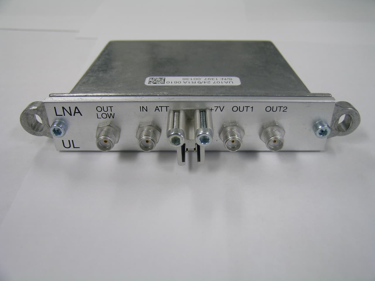
E675JS0120
Aug 26, 2010Nexus Dual Band Repeater
Equipment Class
TNB - Licensed Non-Broadcast Station Transmitter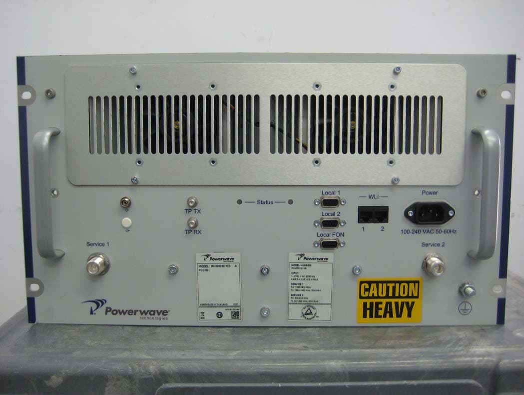
E675JS0119
Aug 01, 2010Nexus Dual Band Repeater
Equipment Class
PCB - PCS Licensed Transmitter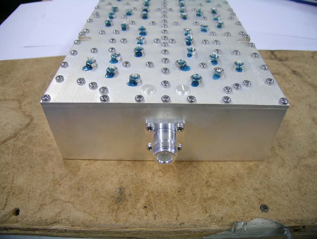
E675JS0118
Jul 26, 2010Nexus Dual Band Repeater
Equipment Class
PCB - PCS Licensed Transmitter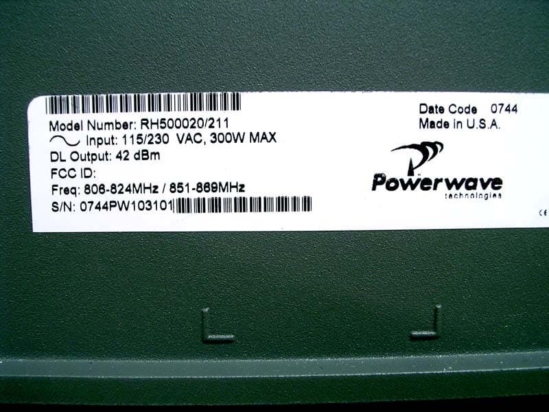
E675JS0096
Jan 10, 2008Wideband Radio Head
Equipment Class
TNB - Licensed Non-Broadcast Station Transmitter