E675JS0054RF Front End Multi-Carrier Power Amplifier System
Powerwave Technologies Inc
Click to zoom
Application Details
- Equipment Class
- AMP - Amplifier
- Date of Grant
- Aug 14, 2001
- Application Purpose
- Original Equipment
- Date of Application
- Jul 08, 2001
- Equipment Note
- RF Front End Multi-Carrier Power Amplifier System
- Frequency Range
- 1930.00000000 - 1945.00000000
- Company
- Powerwave Technologies Inc
- Country
- United States
Documents & Files
Document Text
Text extracted from the exhibit documents filed with the FCC. Open a document above to read the original.
Users Manual
DraftRX 1850-1910 MHz; TX 1930-1945 MHz 044-05082 Rev. AMarch 2001 System Integration Manual Radio Frequency Front End Multi-Carrier Power Amplifier System DraftRF Front End System Integraton Manual 044-05082 Rev. A ii March 2001 March 2001 Powerwave Technologies, Inc.Tel: (714) 466-1000 1801 E. St Andrew PlaceFax: (714) 466-5800 Santa Ana, CA 92705Web Site: www.powerwave.com ® © 2001 Powerwave Technologies Incorporated. All rights reserved. Powerwave Technologies, and the Powerwave logo are registered trademarks Powerwave Technologies, Inc. reserves the right to make changes to the documentation and equipment, including but not limited to component substitution and circuitry changes. Changes that impact this manual may subsequently be incorporated in a later revision of this manual. DRAFTRF Front End System Integration Manual 044-05082 Rev. A 1-1 March 2001 Section 1 General Discription 1-1 Introduction This manual contains information and procedures for installation, operation, and maintenance of the Radio Frequency Front End (RFFE) Multi-Carrier Power Amplifier (MCPA) System. This manual is organized into sections as follows: Section 1.General DescriptionAppendix B: Amplifier Power Setting Procedure Section 2. InstallationAppendix C: General Site Survey Form Section 3. Operating Instructions Section 4. Principles of Operation Section 5. Maintenance Section 6. Troubleshooting 1-2 General Discription Designed to compensate for cable loss due to long cable runs, the RFFE uses an AB amplifier that utilizes a pre-distortion technique for linearization (see figure 4-3 for the amplifier block dia- gram). Designed as a two unit system and equipped with a space diversity path to reduce fading, the RFFE operates in the PCS frequency range of: 1850MHz to 1910MHz (receive) and 1930MHz to 1945MHz (transmit): The system consists of. • The Masthead Unit (MHU) • The Masthead Unit Interface (MHUI) 1-2.1 The Masthead Unit The primary function of the MHU is to provide maximum RF output power (not to exceed 100 Watts) with multiple CDMA carries into a matched 50 Ohm load while maintaining the spectral re- growth and spurious requirements (see table 1-2). Supported by a mounting frame (see figure 1-2), the Mast Head Unit (MHU) is mounted on the antenna tower near the antenna and consists of three modular components; the common box and two RF transmit (Tx) modules. each module is encased in a weatherproof (NEMA 4) housing (refer to table 1-2 for environmental specifica- tions). 1-2.1.1 The Common Box The common box (see figure 1-4) connects to both Tx modules via blind mate connectors (refer to figure 1-1 and table 1-1). It houses a redundant LNA path, two input duplexers, two output du- plexers, two 27VDC (scalable up to 1200Watts) power supplies, and a control board. 1-2.1.2 The Transmitt Modules Powered by 220VAC from the host breaker panel, the two RF transmit modules are used for re- dundancy in the system. Each module houses one MPA9505-55 MCPA and a rectifier circuit that reduces the 220VAC to the 27VDC required to operated the amplifier. To aid in maintaining the system’s operating temperature, each amplifier is mounted on a heat sink and is equipped with a 220VAC variable speed fan. Refer to figure 1-5. The MHU connects to the Masthead Unit Interface (MHUI) by two RF cables, and one CONTROL cable. Refer to figure 2-6. DRAFTRF Front End System Integration Manual 044-05082 Rev. A 1-2 March 2001 1-2.1.3 Masthead Unit Interface The Masthead Unit Interface (MHUI) interfaces the MHU to the host base station. It provides a user friendly control panel for power level adjustment and display. The control panel is key activated and displays major, critical and minor alarm conditions via LED displays. Refer to sec- tion 2 for a more detailed description of the MHUI controls. The enclosure houses a low power duplexer, a control board, the control panel, cell size variable attenuators (both Rx and Tx) and a preamp. The system reports and displays alarm faults to the external summary module via an RS-485 bus or form C dry contact relays. Refer to figure 4-4 for the MHUI functional block diagram. The MHU-MHUI pair operates between 1dB and 16dB of cable loss in the transmit/receive coaxial cable. Therefore, the maximum distance between the MHU and MUI depends on the cable type used (e.g. 7/8”, 1/2” or 1/4” foam-dielectric coaxial cable). Note: The Connector Identification (A,B and C) is for reference only and not necessarily labled on the actual connector Figure 1-1 Masthead Unit Blind mate Connector Interface Table 1-1 Blindmate Connector Pin Designation PinFunction 1A+26 VDC 2A+12 VDC 3A-8 VDC 4ACOM 5A-12ANot used 1BNot used 2BTX IN 3BTX OUT 4BNot used 1CMute 2C-4CNot used 5CRS-485H 6CRS-485L 7CCOM 8C-12CNot used 1 2 3 4 1 6 1 6 7 1212 7 AB C DRAFTRF Front End System Integration Manual 044-05082 Rev. A 1-3 March 2001 Table 1-2 System Specifications with the MPA9505-55 MCPA Frequency: Receive Transmit 1850-1910 MHz 1930-1945 Mhz RF Input Power3dBm (2 milliWatts) RF Output Power:55 Watts (47.40 dBm) Max./ 7carriers Nominal Gain 40 dB ±1.0 dB Typical Gain Flatness ±0.2 dB (over any 2.0 MHz in band) Gain Variation Over Temperature1.0 dB @ -20 to 80 ºC Base Plate IMD Spurious Emissions @ 7 carriers (Room Temperature): Frequency Off-Set ± 885 KHz Frequency Off-Set ± 1.25 MHz Frequency Off-Set ± 2.25 MHz -47 dBc max (30 KHz BW) -13 dBm max (12.5 KHz BW) -40 dBc (marker to marker) IMD Spurious of MCPA in MHU @ An- tenna Port: 885 KHz, 30 KHz BW 1.98 MHz, 30 KHz BW 2.25 MHz, 1 MHz BW -47 dBc -57 dBc -15 dBm Spectrum Regrowth of MCPA in MHU @ Antenna Port: 885 KHz 1250 MHz 2250 KHz -47 dBc -13 dBm -13 dBm Tx Noise in Rx Band @ MCPA Output:-122 dBm/Hz (max.) Tx Power in Rx Band @ MHUI Rx Output-110 dBm @ Rated Output Power Input/Output VSWR1.3 : 1 Output ProtectionMismatch Protected DC Power 27 VDC ± 1.0 VDC @ 24 Amps max. Sample Port-40 dB ±1.0 dB Operating Temperature -20 °C to 85 °C Base Plate Storage Temperature -40 ºC…
Text truncated - open the document above for the full version.
Attestation Statements
TÜV PRODUCT SERVICE 10040 Mesa Rim Road San Diego, CA 92121-2912 Phone 858 546 3999 FAX 858 546 0364 Report No. 0258-06 Page 10 of 10 Rev.No 1.0 GENERAL REMARKS: NOTE: All photographs are representative of setup for maximum emissions. (*) Radiated Emissions - all levels are ambient measurements. (*) Equivalent Radiated Emissions - no emissions detected above 2nd Harmonic. SUMMARY: All tests according to the regulations cited on page 3 were n - Performed o - Not Performed The Equipment Under Test n - Fulfills the general approval requirements cited on page 3.* o - Does not fulfill the general approval requirements cited on page 3. Statement of Measurement Uncertainty The data and results referenced in this document are true and accurate. The measurement uncertainty is calculated to be ±2 dB for conducted emissions and ±4 dB for radiated emissions. Equipment Received Date:28 June 2000 _______________________ Testing Start Date:28 June 2000 _______________________ Testing End Date:28 June 2000 _______________________ - TÜV PRODUCT SERVICE, INC. - Responsible Engineer:Responsible Engineer: Dave MarshallJim Owen (EMC Test Engineer)(EMC Lead Engineer)
Block Diagram
RF Front End System Functional Block Diagram Power Amplifier Module Functional Block Diagram Cable DiplexerDiplexer Dr. Dr. PD PD HPA HPA VVA Box MHUMHUI Diplexer Cable run from base station to masthead RX PathRX PathRX Path RF Input 1930 - 1945 MHz MPA9505-55 MPA9505-55 Pre Amp Pre Main Main Amp Error Amp Delay Feed Forward Loop control 2nd Loop Phase & Gain 1st Loop Phase & Gain Delay Alarms & Display +15 +5 -5 Power Supply -30dB -10dB -40dB RF Out RFL PWR FWD PWR Front Panel Smart Rack +27VDC RF Input 1930 - 1945 MHz
Cover Letter(s)
Question 1: No intermodulation data: This test was performed and was inadvertantly omitted from the report. Upon discussion with you, however, the p0lot taken did not appear to be sufficient for approval of the system. We discussed several options as the actual bandwidth of the signal is 6 MHz wide and the band being applied for is only 15 MHz wide. The following data records are included: PLOTS A) Shows 20 dB bandwidth or one signal is 6.2 MHz. B) Shows 3 simultaneous signals bandwidth of all three 21.18 Hz. The band being applied for is only 15 MHz wide (1930 - 1945 MHz). C) 1 signal at 55 W D) 2 signals at 55 W each E) 3 signals at 55 W each F) 7 plots showing no obvious intermodulation products in either side when 3 signals applied. The first plot sent using two-tone intermodulations also shows the same results. This should show compliance in the worst case possible scenario. Question 2: Radiated spurious substitution method not used: We discussed this and we are aware that this is a reuqirement; however, since this data was taken in August of last year, before the substitution method had become the standard, we felt it was unnecessary to retake the data. The customer met all the requirements at the time of initial testing. We are aware that for all licensed devices, signal substitution is required and will be applied in all future submissions. Question 3: Equipment label: In our discussion, I clarified that the amplifier is a device installed into another client’s enclosure and the only obvious place for the FCC label was on the top cover of the unit. The picture provided seemed to add to the confusion and an explanation should have been supplied.
External Photos
BOTTOM OF UNIT INPUT CONNECTOR VIEW OUTPUT CONNECTOR VIEW
Internal Photos
COMBINER BOARD BACK COMBINER BOARD FRONT A COMBINER BOARD FRONT B COMBINER BOARD FRONT C COMBINER FRONT FULL DIGITAL BOARD BACK DIGITAL BOARD FRONT DRIVER BOARD BACK DRIVER BOARD FRONT MHUPA ISOVIEW1 MHUPA ISOVIEW2 MHUPA PWR SUPPLIES IN FAN BOARD 1 MHUPA TOPVIEW1 PALLET BOARD BACK PALLET BOARD FRONT PRE D BACK PRE D FRONT SPLITTER BOARD BACK SPLITTER BOARD FRONT A SPLITTER BOARD FRONT B SPLITTER BOARD FRONT C SPLITTER FRONT FULL TOP COVER OPEN TOP VIEW WITHOUT DIGITAL BOARD
Operational Description
Operating Instructions Introduction This section contains a functional description of the Powerwave Technologies, Inc.’s RFFE Multi- Carrier Power Amplifier System. Refer to Figure 1 for the system’s functional block diagram. RF INPUT Signal The maximum input power for all carrier frequencies should not exceed the limits specified in section 1, table 1-2 of this manual. For proper amplifier loop balance, the out of band components of the input signals should not exceed -60 dBc. The input VSWR should be 2:1 maximum (or better). RF OUTPUT Load The load impedance should be as good as possible (1.5:1 or better) in the working band for good power transfer to the load. If the amplifier is operated into a filter, it will maintain its distortion characteristics outside the signal band even if the VSWR is infinite, provided the reflected power does not exceed one watt. A parasitic signal of less than one Watt incident on the output will not cause distortion at a higher level than the normal forward distortion (i.e. -60 dBc). System Functional Description A two piece design, the RF Front End (RFFE) Multi-Carrier Power Amplifier system is comprised of a Mast Head Unit (MHU) which is installed on the antenna tower and a Mast Head Unit Interface (MHUI) that is installed in the host base station. The MHU is comprised of two transmit modules for redundancy and a common box assembly. Each transmit module houses one MPA8503-55 power amplifier and one 27 Vdc, 1200 Watt power supply. Powered by 220 Vac from the host base station, each module is equipped with a 220 Vac variable speed fan to maintain the system’s operating temperature. The common box mates the two amplifiers via blind mate connectors. Mounted in a support frame to withstand heavy wind loads, the common box houses a redundant LNA path, I/P O/P duplexers, receiver filter, a two-way power splitter, an active combiner and a control module. The RF IN, RF OUT, +27 Vdc and the ALARM summary connector, interface with the host system via the rear panel of the MHUI. The MHUI is the interface between the RFFE system and the host base station. The MHUI reports alarms via the RS-485 bus or form-C interface and displays alarms using an LED display. The MHUI houses a low power duplexer, control board, the system control panel, a preamp, and the cell size variable attenuators (both transmit and receive). A composite RF signal from the base station radios is applied to J2 (TX/RX) at the rear of the control panel. From there the signal passes through a voltage variable attenuator (VVA), then a two-way splitter. Each leg of the splitter passes through an isolator, then the blind-mate connector to interface with the MCPA. The signal then returns to the MHUI via the blind-mate connector after being amplified by the MCPA modules. The two high-power signals are combined by the active power combiner. The active power combiner has the capability of switching MCPA channels off-line by the use of RF switches. If an MCPA is not present, turned off, or faulted, the switch will open in that channel and physically disconnect that MCPA. The combiner maintains its low insertion characteristics when used in the single path configuration. Note that the splitter is not switched, therefore the power is automatically reduced by 3 dB, thus eliminating an output overdrive condition. The output of the combiner is fed through a coupler, then a receive-band filter. The amplified RF signal is available for use at the output of the receive-band filter (J2). The coupler is used to sample the output power to the true RMS detector. The true RMS detector will supply the microcontroller with an accurate average power regardless of the signal modulation type. The dynamic range is 25 dB. The power reading is used during the gain initialization phase when deploying the system or monitoring to detect excessive output power. In both cases the VVA will be adjusted accordingly. Two non-RF features of the RFFE system are inrush current limiting and alarm status/serial interface ports. The inrush current limiting circuitry is used to minimize the instantaneous current demand when the MCPA is first DC powered-up. This is due to the high capacitance on the MCPA’s DC input. The circuit is placed in series on the DC source before the MCPA. Voltage for the MHU is derived prior to the in-rush current limit circuitry. The circuitry is in a high impedance state upon DC power-up. When an MCPA is enabled the impedance is slowly brought down to nearly 0 ohms. This will allow the capacitors to charge over a longer period of time, thus reducing the high current drain on the power supply. The three ports on the rear of the subrack are for Form-C alarms (J1), RS-485/Addressing serial communication (J7) and RS-485 and RS-232 serial communication (J8). The J1, J7, and J8 connectors are detailed in chapter 2 (see figures 2-2, 2- 3, and 2-4, and tables 2-2, 2-3, and 2-4). The serial interface allows the user to acquire MCPA internal voltages and status, exercise MCPA and VVA control, upgrade MCPA or subrack firmware, and obtain true RMS power readings. Figure 1RF Front End System Functional Block Diagram Transmit Modules Power output specifications for a one or two module system are listed in section 1, table1-1. Each amplifier is a self-contained plug-in module and is functionally independent of other amplifier modules. The amplifier modules are designed for parallel operation to achieve high peak power output, and for redundancy in unmanned remote locations. The MPA8503-55 amplifier is a linear, feed-forward power amplifier that operates in the 25 MHz frequency band from 1930 to 1945 MHz. Cable DiplexerDiplexer Dr. Dr. PD PD HPA HPA VVA Box MHUMHUI Diplexer Cable run from base station to masthead RX PathRX PathRX Path Printed By: Sara ReevesCompany Confidential - Uncontrolled CopyDate Printed: 21-May-2001 10:13:33 Number: DATP-500-01084-003Rev: B ECO-11347Status: Production DOCUMENT NUMBER: ATP 500-01084 Page 1 of 9…
Text truncated - open the document above for the full version.
RF Exposure Info
FCC Equipment Authorization Application Exhibit Type of Exhibit:Statement Concerning RF Exposure FCC Rule Part:47 CFR 1.1307 Manufacturer:Powerwave Technologies Per the FCC Rules and Regulations as described in OET Bulletin 65, this device is categorically excluded from routine evaluation because these are used at fixed installations with antennas mounted on outdoor, permanent structures and fall well below the power limits requiring RF evaluation in accordance with 47 CFR 1.1307.
Test Report
TÜV PRODUCT SERVICE 10040 Mesa Rim Road San Diego, CA 92121-2912 Phone 858 546 3999 FAX 858 546 0364 Report No. 0258-03 (FCC ID: E675JS0054) Page 1 Rev.No 1.0 MEASUREMENT AND TECHNICAL REPORT POWERWAVE TECHNOLOGIES 2026 McGaw Avenue Irvine, CA 92614 DATE: 14 June 2001 This Report Concerns:Original Grant: XClass II Change: Equipment Type:Powerwave RF Front End System Deferred grant requested per 47 CFR 0.457(d)(1)(ii)?Yes: Defer until: No: X Company Name agrees to notify the Commission by:N/A of the intended date of announcement of the product so that the grant can be issued on that date. Transition Rules Request per 15.37?Yes:*No: X (*) FCC Part 2, Paragraphs 2.1046, 2.1051, 2.1053, and Part 24, Paragraph 24.238 Report Prepared by: TÜV PRODUCT SERVICE 10040 Mesa Rim Road San Diego, CA 92121-2912 Phone: 858 546 3999 Fax: 858 546 0364 TÜV PRODUCT SERVICE 10040 Mesa Rim Road San Diego, CA 92121-2912 Phone 858 546 3999 FAX 858 546 0364 Report No. 0258-03 (FCC ID: E675JS0054) Page 2 Rev.No 1.0 TABLE OF CONTENTS Pages 1 GENERAL INFORMATION3 1.1Product Description3 1.2Related Submittal Grant3 1.3Tested System Details3 1.4Test Methodology4 1.5Test Facility4 1.6Part 2 Requirements5 2 SYSTEM TEST CONFIGURATION6 2.1Justification6 2.2EUT Exercise Software6 2.3Special Accessories6 2.4Equipment Modifications6 2.5Configuration of Tested System6 3RADIATED EMISSION DATA/EQUIPMENT7 Field Strength Calculation12 4 CONDUCTED EMISSION DATA/EQUIPMENT13 5ATTESTATION STATEMENT41 TÜV PRODUCT SERVICE 10040 Mesa Rim Road San Diego, CA 92121-2912 Phone 858 546 3999 FAX 858 546 0364 Report No. 0258-03 (FCC ID: E675JS0054) Page 3 Rev.No 1.0 1 GENERAL INFORMATION 1.1Product Description Pcs Rx and TX Booster System Powerwave RF Front End System Configuration tested was with CDMA modulation only. An output bandpass filter or duplexer was used with a minimum rejection of 50 dB between the Rx and Tx bands and an output power rating of 150W CW. Voltage: 220 Vac; 1 phase; Current: 7A; Current 5.75 Unit tested at the input/output RF interface provided by the test connector supplied by Advantech. Typical Installation: PCS network operator’s cell sites. Mounted on tower. EUT Power Cable: Permanent, Shielded EUT Interface Ports and Cables EUT I/O Ports and Cables: RF Input; analog; quantity 1; no shielding; coaxial termination; characteristic impedance port termination; connector type - metallized 9-pin D-sub. RF Output; analog and digital; quantity 1; no shielding; coaxial termination; 50-ohm port termination; connector type - N type. RS-485; digital; quantity 1; no shielding; 9 poles termination; 05 ohms port termination; connector type - DB9 AC supply; analog; quantity 1; no shielding; 3 poles termination; port termination - N/A; connector type - MIL-C 1015. Mute control; digital; quantity 1; no shielding; toggle switch termination; Operating Description: Amplifer enabled, applying test signal adjusted to measure rated power at the output using a RMS power meter. Test signal IS95 - 1 carrier 9 users 11 dB crest factor. DESCRIPTION:Power amplifier module MODEL NUMBER:0001 SERIAL NUMBER:0001 DESCRIPTION:PA module test connector 1.2Related Submittal/Grant None 1.3Tested System Details The FCC IDs for all equipment, plus descriptions of all cables used in the tested system are: None TÜV PRODUCT SERVICE 10040 Mesa Rim Road San Diego, CA 92121-2912 Phone 858 546 3999 FAX 858 546 0364 Report No. 0258-03 (FCC ID: E675JS0054) Page 4 Rev.No 1.0 1.4Test Methodology Purpose of Test:To demonstrate compliance with the ANSI C63.4 setup. Test Performed:X1. Conducted Emissions, FCC Part 2, Paragraphs 2.1051 and Part 24, Paragraph 24.238 2. Radiated Emissions EN55022: 1992 Class B limit, 30 - 1,000 MHz, 10 meters X3. Radiated Emission per FCC Part 2, Paragraph 2.1053, & Part 24, Paragraph 24.238 4. Engineering evaluations 5. Frequency Stability, Part 2, Paragraph 2.995, and Part 87, Paragraph 87.133 X6. RF Output Power, 2.1046 Both Conducted and radiated testing were performed according to the procedures in FCC/ANSI C63.4 and CSA 108.8 - M1983. Radiated testing was performed at an antenna-to-EUT distance of 3 meters (1 - 10 GHz). 1.5Test Facility The open area test site and conducted measurement data were tested by: TÜV PRODUCT SERVICE 10040 Mesa Rim Road San Diego, CA 92121-2912 Phone: 858 546 3999 Fax: 858 546 0364 The Test Site Data and performance comply with ANSI 63.4 and are registered with the FCC, 7435 Oakland Mills Rd, Columbia Maryland 21046. All Measurement Data is acquired according to the content of FCC Measurement Procedure and ANSI C63.4, unless supplemented with additional requirements as noted in the test report. TÜV PRODUCT SERVICE 10040 Mesa Rim Road San Diego, CA 92121-2912 Phone 858 546 3999 FAX 858 546 0364 Report No. 0258-03 (FCC ID: E675JS0054) Page 5 Rev.No 1.0 1.6 Part 2 Requirements Type of Emission: F9W Freq. Range: 1930 - 1945 MHz Range of operating power values: 0 - 55 W DC voltages: 27 V / 24 A Equipment an AM broadcast stereophonic exciter-generator : N/A TÜV PRODUCT SERVICE 10040 Mesa Rim Road San Diego, CA 92121-2912 Phone 858 546 3999 FAX 858 546 0364 Report No. 0258-03 (FCC ID: E675JS0054) Page 6 Rev.No 1.0 2.SYSTEM TEST CONFIGURATION 2.1Justification The EUT was initially tested for FCC emission in the following configuration: See Block Diagram. 2.2EUT Exercise Software None 2.3Special Accessories None 2.4Modification None 2.5Configuration of Tested System See Block Diagram. TÜV PRODUCT SERVICE 10040 Mesa Rim Road San Diego, CA 92121-2912 Phone 858 546 3999 FAX 858 546 0364 Report No. 0258-03 (FCC ID: E675JS0054) Page 7 Rev.No 1.0 3RADIATED EMISSION DATA The following data lists the significant emission frequencies, measured levels, correction factor (which includes cable and antenna corrections), the corrected reading, and the limit. See following page(s). TÜV PRODUCT SERVICE 10040 Mesa Rim Road San Diego, CA 92121-2912 Phone 858 546 3999 FAX 858 546 0364 Report No. 0258-03 (FCC ID: E675JS0054) Page 11 Rev…
Text truncated - open the document above for the full version.
Test Setup Photos
TÜV PRODUCT SERVICE 10040 Mesa Rim Road San Diego, CA 92121-2912 Phone 858 546 3999 FAX 858 546 0364 Report No. 0258-06 Page A2 of A4 Rev.No 1.0 Photograph of Test Setup: Conducted Emissions 10/150/450 kHz - 30 MHz TÜV PRODUCT SERVICE 10040 Mesa Rim Road San Diego, CA 92121-2912 Phone 858 546 3999 FAX 858 546 0364 Report No. 0258-06 Page A3 of A4 Rev.No 1.0 Photograph of Test Setup: Radiated Emissions 30 MHz - 1000 MHz TÜV PRODUCT SERVICE 10040 Mesa Rim Road San Diego, CA 92121-2912 Phone 858 546 3999 FAX 858 546 0364 Report No. 0258-06 Page A4 of A4 Rev.No 1.0 Photograph of Test Setup: Radiated Emissions 30 MHz - 1000 MHz Conducted Spurious Spectrum Analyzer Power Divider Attenuator Directional Coupler Output Input Coupled EUT RF RF Output Input Signal Generator RF Output Variable Attenuator Driver RF In RF Out Isolator In Out Power Sensor Variable Attenuator Power Sensor Power Meter Directional Coupler 30 dB Load Attenuator Input Input/Output Plots Power Meter Power Divider Attenuator Directional Coupler Output Input Coupled EUT RF RF Output Input Signal Generator RF Output Variable Attenuator Driver RF In RF Out Isolator In Out Spectrum Analyzer Power Sensor Attenuator Variable Attenuator Power Sensor Power Meter Directional Coupler 30 dB Load Attenuator Input
Contact Information
Applicant
Jeff Dale(Principal Reliability Engineer)
Test Firm
TUV AmericaJames Owen
Technical Specifications
| # | Rule Parts | Frequency Range | Power Output | Emission |
|---|---|---|---|---|
| 1 | 24E | 1.93 GHz - 1.95 GHz | 55 W | F9W |
Other Applications from Powerwave Technologies Inc
E675JS0123
Nov 03, 2011Multi-carrier RF Power Amplifier
Equipment Class
AMP - Amplifier
E675JS0120
Aug 26, 2010Nexus Dual Band Repeater
Equipment Class
TNB - Licensed Non-Broadcast Station Transmitter
E675JS0119
Aug 01, 2010Nexus Dual Band Repeater
Equipment Class
PCB - PCS Licensed Transmitter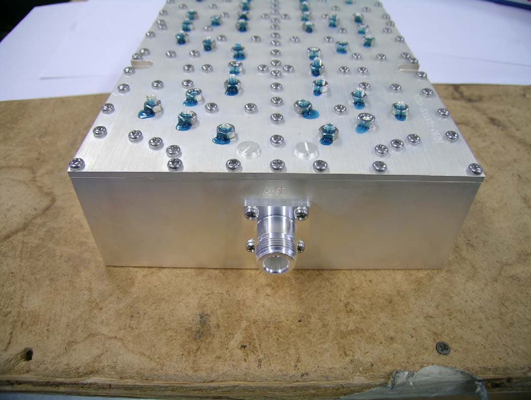
E675JS0118
Jul 26, 2010Nexus Dual Band Repeater
Equipment Class
PCB - PCS Licensed Transmitter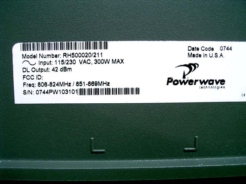
E675JS0096
Jan 10, 2008Wideband Radio Head
Equipment Class
TNB - Licensed Non-Broadcast Station Transmitter