E675JS0055PCS 1900 MHz Single Channel Power Amplifier
Powerwave Technologies Inc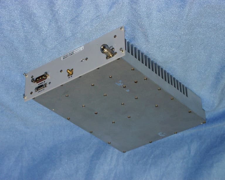
Click to zoom
Application Details
- Equipment Class
- AMP - Amplifier
- Date of Grant
- Jul 30, 2001
- Application Purpose
- Original Equipment
- Date of Application
- Jul 30, 2001
- Equipment Note
- PCS 1900 MHz Single Channel Power Amplifier
- Frequency Range
- 1930.00000000 - 1990.00000000
- Company
- Powerwave Technologies Inc
- Country
- United States
Documents & Files
Document Text
Text extracted from the exhibit documents filed with the FCC. Open a document above to read the original.
Users Manual
OPERATING INSTRUCTIONS NTQA50GA Note: These operating instructions describe the procedure for turning on and off the amplifier output power using signal generators. This amplifier will be used with transmitters which have been or will be certified separately. The specific transmitter instruction book should be consulted for the correct method to use this amplifier with transmitters. 1. The input voltage range, applied to pin A1 of the DC input connector, should be between –36VDC and –57 VDC. Pin A2 and A3 of the connector should be grounded. 2. Pin 5 of the Data I/O connector should be grounded to enable operation of the amplifier without the data interface. Pins 1, 2, 11, and 12 on the Data I/O connector are connected to ground. Operation with the Data I/O interface can only be performed using the transmitter software. See the transmitter manual for instructions. 3. Connect the RF signal generator to the RF input port. 4. Connect the RF output port to the measurement equipment. Make sure the measurement equipment is capable of handling 33 watts, or use a power attenuator or directional coupler to attenuate the signal to a level the equipment can handle. 5. To turn on the amplifier, first apply the DC voltage with the specified range (-48 VDC nominal). 6. Apply RF power from the signal generator. Adjust the RF input power until the desired RF output power is achieved. The amplifier’s maximum RF output power rating is 33 watts (+45.2 dBm) 7. The gain may change up to 0.5 dB as the amplifier temperature stabilizes after turn-on. Let the amplifier warm up for 10-30 minutes, then re-adjust the power to compensate for the gain change. 8. The amplifier is now operational. SPECIFICATIONS Parameter Specification Operating Frequency 1930 to 1990 MHz Rated Output Power +45.2 dBm (33 Watts) Gain at Full Power 48 +/- 1 dB Input Voltage Range -36 to –57 VDC Maximum DC Power Consumption 230 Watts Channeling Controlled by transmitter Modes of Transmission GSM or EDGE Type of Modulation Not applicable (performed by transmitter) Occupied Bandwidth and Emissions Designators Emissions Type Amplitude Frequency Removed from Carrier GSM (300KGXW) -30 dBc 200 kHz -33 dBc 250 kHz -60 dBc 400 kHz -70 dBc 600 kHz -73 dBc 1200 kHz -75 dBc 1800 kHz -80 dBc 6000 kHz EDGE (300KG7W) -30 dBc 200 kHz -33 dBc 250 kHz -56 dBc 400 kHz -70 dBc 600 kHz -73 dBc 1200 kHz -75 dBc 1800 kHz -80 dBc 6000 kHz
Cover Letter(s)
From: Pete Krebill Sent: Thursday, July 26, 2001 2:21 PM To: CERTADM Cc: CERTADM; Mike Kuo; Steve Cheng; Anne Liang Subject: FW: Powerwave Technologies Inc., FCC ID:E675JS0055, AN01T1432 Mike, In response to questions 2 and 3: the emissions you questioned, at 1997MHz, are fundamental emissions and are not subject to the -13dBm limit. Due to the spectral limitations of the spectrum analyzer, when using a large frequency span, the displayed marker frequency is not exact. During the block edge and output bandwidth measurements, all of the fundamental emissions were verified to be at the frequencies stated in the test report and are all within the liscensed band for FCC part 24. Regards, Pete Krebill -----Original Message----- From: Steve Cheng Sent: Thursday, July 26, 2001 1:37 PM To: Pete Krebill Subject: FW: Powerwave Technologies Inc., FCC ID:E675JS0055, AN01T1432 -----Original Message----- From: Mike Kuo Sent: Thursday, July 26, 2001 1:16 PM To: Steve Cheng Cc: Anne Liang Subject: RE: Powerwave Technologies Inc., FCC ID:E675JS0055, AN01T1432 -----Original Message----- From: CERTADM Sent: Thursday, July 26, 2001 1:15 PM To: Steve Cheng Cc: Anne Liang; Mike Kuo Subject: Powerwave Technologies Inc., FCC ID:E675JS0055, AN01T1432 Notice_content ------------- Question #1: Please provide Operational Description and Tune-Up procedures. Question #2: Page 29 of test report, out of band emission for EDGE modulation. 1997MHz is over the -13dBm limits. Please address this non-compliance emission. Question #3: Page 38 of test report, out of band emission for GSM modulation. 1997Mhz is over the -13dBm limits. Please address this non-compliance emission. Best Regards Mike Kuo / TCB Certifier The items indicated above must be submitted before processing can continue on the above referenced application. Failure to provide the requested information within 60 days of the original e-mail date may result in application dismissal and forfeiture of the filing fee. Also, please note that partial responses increase processing time and should not be submitted. Any questions about the content of this correspondence should be directed to the e-mail address listed below the name of the sender.
Cover Letter(s)
TCB RF Exposure Review Procedure Statement FCC ID:E675JS0055 Transmitter Category Device Type Product Category Approval and Review Procedures Used Specific Procedures: I Amplifier Fixed Transmitters identified in Table 1 of §1.1307 Section A SP(9) Grant Condition : Emissions listed correspond to GSM and EDGE operations. The antenna(s) used for this transmitter must be fixed-mounted on outdoor permanent structures. RF exposure compliance is addressedat the time of licensing, as required by the responsible FCC Bureau(s), including antenna co-locationrequirements of §1.1307(b)(3). SP9 Grant conditions have been reviewed by TCB and has made the determination that device complied with RF Exposure review procedures. Reviewed by Mike KuoCompliance Certification ServicesJuly 31, 2001
ID Label/Location Info
POWERWAVE TECHNOLOGIES INCORPORATED CANADA: FCC ID: E67 5JS0055 XX
Operational Description
OPERATING INSTRUCTIONS NTQA50GA Note: These operating instructions describe the procedure for turning on and off the amplifier output power using signal generators. This amplifier will be used with transmitters which have been or will be certified separately. The specific transmitter instruction book should be consulted for the correct method to use this amplifier with transmitters. 1. The input voltage range, applied to pin A1 of the DC input connector, should be between –36VDC and –57 VDC. Pin A2 and A3 of the connector should be grounded. 2. Pin 5 of the Data I/O connector should be grounded to enable operation of the amplifier without the data interface. Pins 1, 2, 11, and 12 on the Data I/O connector are connected to ground. Operation with the Data I/O interface can only be performed using the transmitter software. See the transmitter manual for instructions. 3. Connect the RF signal generator to the RF input port. 4. Connect the RF output port to the measurement equipment. Make sure the measurement equipment is capable of handling 33 watts, or use a power attenuator or directional coupler to attenuate the signal to a level the equipment can handle. 5. To turn on the amplifier, first apply the DC voltage with the specified range (-48 VDC nominal). 6. Apply RF power from the signal generator. Adjust the RF input power until the desired RF output power is achieved. The amplifier’s maximum RF output power rating is 33 watts (+45.2 dBm) 7. The gain may change up to 0.5 dB as the amplifier temperature stabilizes after turn-on. Let the amplifier warm up for 10-30 minutes, then re-adjust the power to compensate for the gain change. 8. The amplifier is now operational. SPECIFICATIONS Parameter Specification Operating Frequency 1930 to 1990 MHz Rated Output Power +45.2 dBm (33 Watts) Gain at Full Power 48 +/- 1 dB Input Voltage Range -36 to –57 VDC Maximum DC Power Consumption 230 Watts Channeling Controlled by transmitter Modes of Transmission GSM or EDGE Type of Modulation Not applicable (performed by transmitter) Occupied Bandwidth and Emissions Designators Emissions Type Amplitude Frequency Removed from Carrier GSM (300KGXW) -30 dBc 200 kHz -33 dBc 250 kHz -60 dBc 400 kHz -70 dBc 600 kHz -73 dBc 1200 kHz -75 dBc 1800 kHz -80 dBc 6000 kHz EDGE (300KG7W) -30 dBc 200 kHz -33 dBc 250 kHz -56 dBc 400 kHz -70 dBc 600 kHz -73 dBc 1200 kHz -75 dBc 1800 kHz -80 dBc 6000 kHz
Test Report
FCC CFR47 PART 24 SUBPART E BROADBAND CERTIFICATION REPORT FOR 1930MHz – 1990MHz SINGLE CHANNEL POWER AMPLIFIER MODEL: NTQA50GA FCC ID: E675JS0055 REPORT NUMBER: 01U0838 ISSUE DATE: 07/20/01 Prepared for POWERWAVE TECHNOLOGIES, INC. 1801 E. ST. ANDREW PLACE SANTA ANA, CA 92705 Prepared by COMPLIANCE CERTIFICATION SERVICES, INC. d.b.a. COMPLIANCE ENGINEERING SERVICES, INC. 561F Monterey Road Morgan Hill, CA 95037-9001 U.S.A. TEL: (408) 463-0885 FAX: (408) 463-0888 PROJECT NO: 01U0838-1 FCC ID: E675JS0055 DATE: JULY 20, 2001 EUT: 1930-1990MHz SINGLE CHANNEL POWER AMPLIFIER PAGE 2 OF 74 COMPLIANCE CERTIFICATION SERVICES DOCUMENT NO:CCSUP4031A 561F Monterey Rd., Morgan Hill, CA 95037-9001, USA TEL:(408) 752-8166 FAX:(408) 752-8168 This report shall not be reproduced except in full, without the written approval of CCS. TABLE OF CONTENTS PAGE 1. FCC CERTIFICATION INFORMATION...................................................................................................3 2. TEST EQUIPMENT LIST.................................................................................................................................6 3. FCC 15 TEST RESULTS...................................................................................................................................6 3.1 PRODUCT DESCRIPTION........................................................................................................................6 3.2 TESTED SYSTEM DETAILS....................................................................................................................7 3.3 EUT SETUP PHOTOS.................................................................................................................................8 3.4 TEST EQUIPMENT LIST.........................................................................................................................10 3.5 RADIATED EMISSION............................................................................................................................11 3.6 CONDUCTED EMISSION.......................................................................................................................12 3.7 EXTERNAL I/O CABLE CONSTRUCTION DESCRIPTION.........................................................12 3.8 CONFIGURATION BLOCK DIAGRAM..............................................................................................13 4. FCC PART 2 CERTIFICATION TEST RESULTS:....................................................................................13 SECTION 2.1046: RF POWER OUTPUT...........................................................................................................14 SECTION 2.1047: MODULATION CHARACTERISTICS............................................................................15 SECTION 2.1049: OCCUPIED BANDWIDTH.................................................................................................15 SECTION 2.1051: SPURIOUS EMISSION AT ANTENNA TERMINAL...................................................20 SECTION 2.1053: FIELD STRENGTH OF SPURIOUS RADIATION........................................................40 SECTION 2.1055: FREQUENCY STABILITY.................................................................................................43 ATTACHMENT 1. SETUP PHOTOS 2. EUT PHOTOGRAPHS 3. INSTALLATION & SERVICE MANUAL 4. SCHEMATIC, PART LISTS & BLOCK DIGRAM 5. PROPOSED FCC ID LABEL FORMAT PROJECT NO: 01U0838-1 FCC ID: E675JS0055 DATE: JULY 20, 2001 EUT: 1930-1990MHz SINGLE CHANNEL POWER AMPLIFIER PAGE 3 OF 74 COMPLIANCE CERTIFICATION SERVICES DOCUMENT NO:CCSUP4031A 561F Monterey Rd., Morgan Hill, CA 95037-9001, USA TEL:(408) 752-8166 FAX:(408) 752-8168 This report shall not be reproduced except in full, without the written approval of CCS. 1. FCC CERTIFICATION INFORMATION The following information is in accordance with FCC Rules, 47CFR Part2, Subpart J, Sections 2.1033 – 2.1055. 2.1033(c)(1): Applicant: POWERWAVE TECHNOLOGIES, INC. 1801 E. ST. ANDREW PLACE SANTA ANA, CA 92705 Contact person: CLINT LAWRENCE Telephone number: (916) 941-3167 2.1033(c)(2) FCC ID: E675JS0055 2.1033(c)(3) Instructions/Installation Manual Refer to Attachment: Installation and Service manual. 2.1033(c)(4) Type of emissions GXW (GSM) G7W (EDGE) 2.1033(c)(5) Frequency Range Transmit: 1930 MHz. to 1990 MHz. 2.1033(c)(6) Range of Operation Power 0 - 33 WATTS 2.1033(c)(7) Maximum Power Rating 33 WATTS. 2.1033(c)(8) Applied voltage and currents into the final transistor elements -48VDC @ 5 Amps maximum 2.1033(c)(9) Tune-up/Optimizations Procedure Refer to Attachment: Installation and Service manual. 2.1033(c)(10)Complete Circuit Diagrams and Functional Diagram Refer to Attachment: Schematics, Parts list & Block Diagram. Confidentiality is requested for these items. PROJECT NO: 01U0838-1 FCC ID: E675JS0055 DATE: JULY 20, 2001 EUT: 1930-1990MHz SINGLE CHANNEL POWER AMPLIFIER PAGE 4 OF 74 COMPLIANCE CERTIFICATION SERVICES DOCUMENT NO:CCSUP4031A 561F Monterey Rd., Morgan Hill, CA 95037-9001, USA TEL:(408) 752-8166 FAX:(408) 752-8168 This report shall not be reproduced except in full, without the written approval of CCS. 2.1033(c)(10a) Means for Frequency Stabilization Not Applicable. Eut is a power amplifier 2.1033(c)(10b) Means for Suppressing of Spurious radiation. Not Applicable. Eut is a power amplifier. 2.1033(c)(10c) Means for Limiting Modulation. Not Applicable. Eut is a power amplifier. 2.1033(c)(10d) Means for Limiting Power. Gain control loop. 2.1033(c)(11)Equipment Identification A drawing of the equipment identification nameplate appears under Attachment: PROPOSED FCC ID LABEL FORMAT. 2.1033(c)(12)Photographs Photographs of the equipment, internal and external views, are found in the Attachment: Eut Photographs. 2.1033(c)(13)Description of Digital Modulation Techniques Not Applicable. Eut is a power amplifier. 2.1033(c)(14) Standard Test Condition The power amplifier was tested under the following conditions. DC Supply Voltage: -4…
Text truncated - open the document above for the full version.
Test Setup Photos
SETUP PHOTOS CONDUCTED EMISSIONS RADIATION FRONT RADIATION BACK SUBSTITUTION SUBSTITUTION
Contact Information
Applicant
Jeff Dale(Principal Reliability Engineer)
Test Firm
Compliance Certification Services IncSteve Cheng
Technical Specifications
| # | Rule Parts | Frequency Range | Power Output | Emission | Tolerance |
|---|---|---|---|---|---|
| 2 | 24 | 1.93 GHz - 1.99 GHz | 33 W | G7W | Amp |
Other Applications from Powerwave Technologies Inc
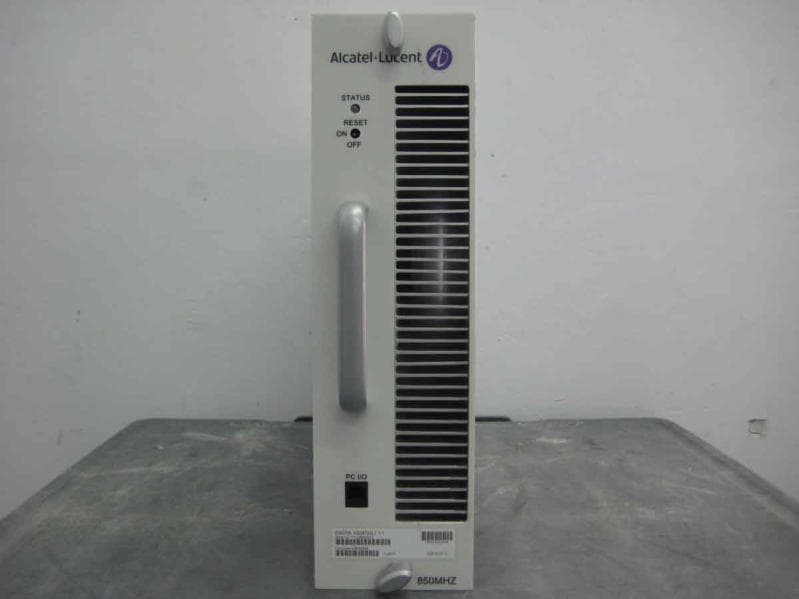
E675JS0123
Nov 03, 2011Multi-carrier RF Power Amplifier
Equipment Class
AMP - Amplifier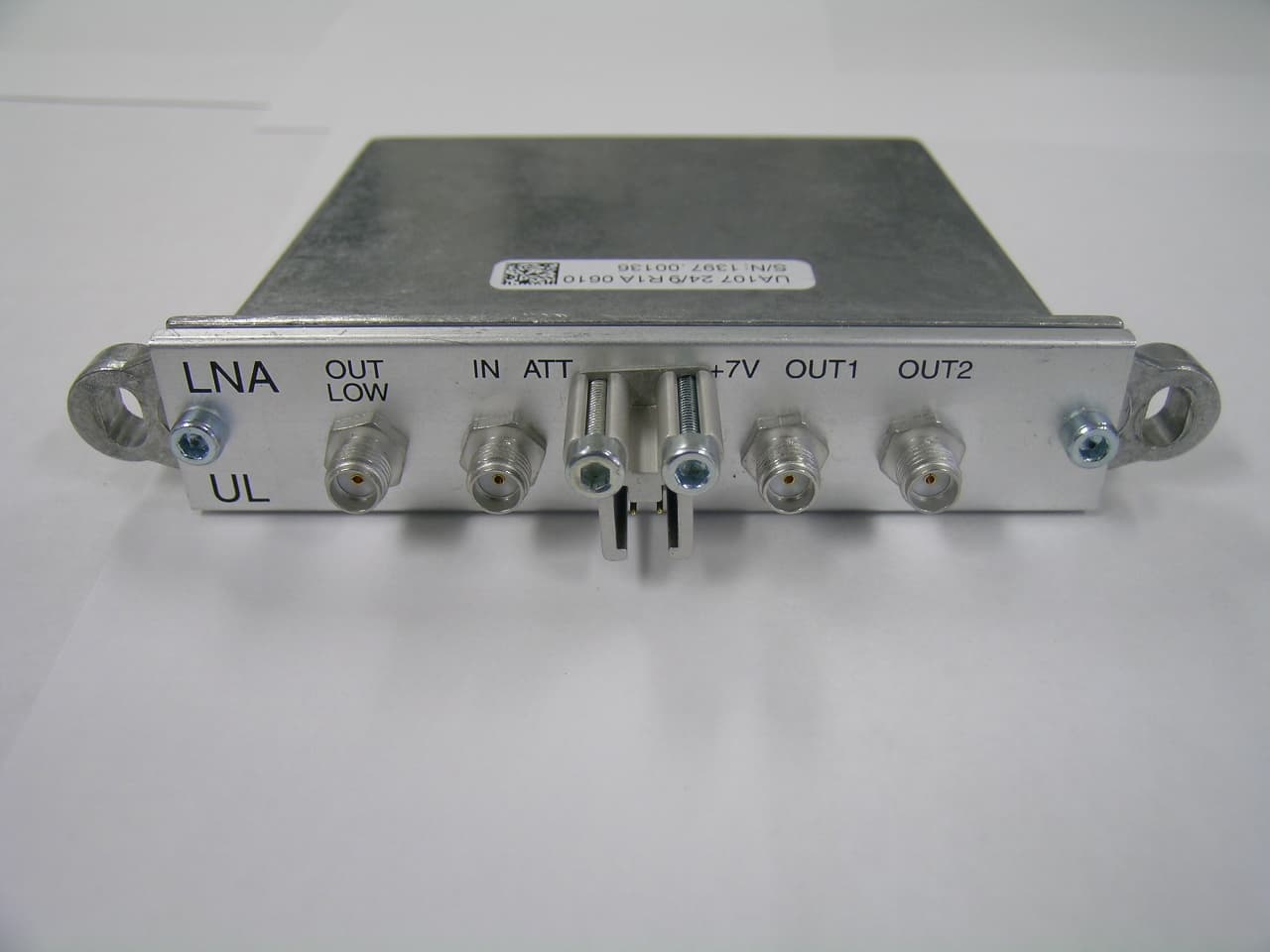
E675JS0120
Aug 26, 2010Nexus Dual Band Repeater
Equipment Class
TNB - Licensed Non-Broadcast Station Transmitter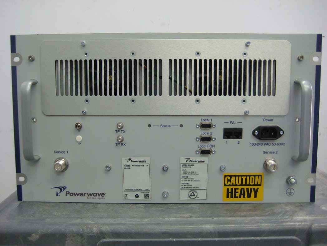
E675JS0119
Aug 01, 2010Nexus Dual Band Repeater
Equipment Class
PCB - PCS Licensed Transmitter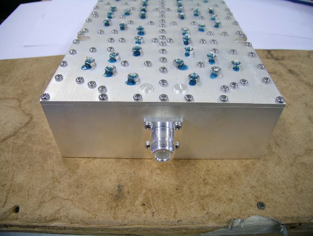
E675JS0118
Jul 26, 2010Nexus Dual Band Repeater
Equipment Class
PCB - PCS Licensed Transmitter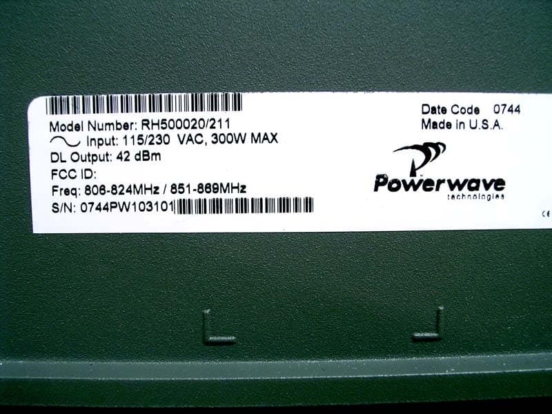
E675JS0096
Jan 10, 2008Wideband Radio Head
Equipment Class
TNB - Licensed Non-Broadcast Station Transmitter