E675JS00591900MHz CDMA Multi-Channel Amplifier
Powerwave Technologies Inc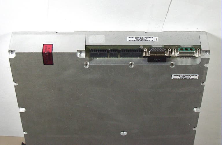
Click to zoom
Application Details
- Equipment Class
- AMP - Amplifier
- Date of Grant
- May 12, 2002
- Application Purpose
- Original Equipment
- Date of Application
- May 12, 2002
- Equipment Note
- 1900MHz CDMA Multi-Channel Amplifier
- Frequency Range
- 1930.00000000 - 1990.00000000
- Company
- Powerwave Technologies Inc
- Country
- United States
Documents & Files
Document Text
Text extracted from the exhibit documents filed with the FCC. Open a document above to read the original.
Users Manual
044-xxxxx Rev. x INSTALLATION & SERVICE MANUAL MULTICHANNEL POWER AMPLIFIER NTGY81AC 1930-1990 MHz 50 WATTS AVERAGE POWER 04 April 2002 Powerwave Technologies, Inc.Tel: (714) 466-1000 1801 E. St. Andrew PlaceFax: (714) 466-5800 Santa Ana, CA 92705Web Site: www.powerwave.com ® 044-xxxxx Rev. x ii TABLE OF CONTENTS Par.Section 1Page No.General DescriptionNo. 1-1Introduction ..................................................................................................................... 1-1 1-2General Description....................................................................................................... 1-1 1-3Functional and Physical Specifications........................................................................... 1-1 Section 2 Installation 2-1Introduction ..................................................................................................................... 2-1 2-2Electrical Service Recommendations ............................................................................. 2-1 2-3Unpacking and Inspection .............................................................................................. 2-1 2-4Installation Instructions ...................................................................................................2-2 2-5+26 VDC Power and Ground Connector P1................................................................... 2-2 2-6Alarms and Sensing Connector P2 ................................................................................ 2-3 2-7Differential IIC Clock, Receive, and Transmit Connector P3.......................................... 2-4 2-8IIC, Power, Alarms,and Controls Connector P4 ............................................................. 2-4 2-9IIC, RS485, Power, and Other Signals Connector P5 .................................................... 2-6 Section 3 Operating Instructions 3-1Introduction ..................................................................................................................... 3-1 3-2Initial Start-Up and Operating Procedures...................................................................... 3-1 Section 4 Principles of Operation 4-1Introduction ..................................................................................................................... 4-1 4-2RF Input Signal ............................................................................................................... 4-1 4-3RF Output Load ..............................................................................................................4-1 4-4Amplifier Functional Description ..................................................................................... 4-1 4-4.1Input Amplifier................................................................................................................. 4-1 4-4.2Predistortion Amplifier ....................................................................................................4-1 4-4.3Driver Amplifier ............................................................................................................... 4-2 4-4.4Main Amplifier ................................................................................................................. 4-2 4-4.5Multifunction Board ......................................................................................................... 4-2 4-5Amplifier Module Cooling................................................................................................ 4-2 4-5Power Distribution...........................................................................................................4-2 044-xxxxx Rev. x iii TABLE OF CONTENTS (Continued) Par.Section 5Page No.Maintenance No. 5-1Introduction ..................................................................................................................... 5-1 5-2Periodic Maintenance ..................................................................................................... 5-1 5-3Test Equipment Required For Test ................................................................................ 5-1 5-4Performance Test ........................................................................................................... 5-2 5-4.1Amplifier Performance Test............................................................................................ 5-2 5-5Field Replacement of the Module................................................................................... 5-5 Section 6 Troubleshooting 6-1Introduction .......................................................................................................................6-1 6-2Troubleshooting................................................................................................................6-1 6-3Return for Service Procedures .........................................................................................6-1 6-3.1Obtaining an RMA ............................................................................................................6-1 6-3.2Repackaging for Shipment ...............................................................................................6-1 LIST OF ILLUSTRATIONS FigurePage No.No. 1-1NTGY81AC Multichannel Power Amplifier ..................................................................... 1-3 2-1+26 Vdc Power and Ground Connector P1 .................................................................... 2-2 2-2Alarms and Sensing Connector P2 ................................................................................ 2-3 2-3Differential IIC Clock, Receive, and Transmit Connector P3.......................................... 2-4 2-4IIC, Power, Alarms, and Controls Connector P4 ............................................................ 2-4 2-5IIC, RS485, Power and Other Connector P5 .................................................................. 2-6 4-1NTGY81AC Multichannel Power Amplifier Functional Block Diagram ............…
Text truncated - open the document above for the full version.
ID Label/Location Info
4.0 1.0 4X R.06 BLANK LABEL INPUT OUTPUT FCC ID MODEL NUMBER DATE CODE LOGO CANADA ID -001 AMPLIFIER NTGY71AA 26VDC, 23.4A MAXIMUM 70W E675JS0047 WEEK/YEAR NORTEL -002 AMPLIFIER NTGY81AA 26VDC, 21.2A MAXIMUM 50W E675JS0046 WEEK/YEAR NORTEL -003 AMPLIFIER NTGY71AB 26VDC, 23.4A MAXIMUM 70W E675JS0047 WEEK/YEAR NORTEL -004 AMPLIFIER NTGY81AB 26VDC, 21.2A MAXIMUM 50W E675JS0046 WEEK/YEAR NORTEL -005 AMPLIFIER NTGY81AC 26VDC, 21.2A MAXIMUM 50W E675JS0059 WEEK/YEAR NORTEL DASH No. PART DESCRIPTION MODEL NUMBER INPUT OUTPUT FCC ID DATE CODE LOGO TABLE 1 2 3. 1. NOTES: UNLESS OTHERWISE SPECIFIED. DRAWING FOR REFERENCE ONLY. ACTUAL LABEL MAY DIFFER FROM DRAWING. MATERIAL: MAKE FROM PWAV P/N 900-00087-001. IMPRINT LABEL WITH INFORMATION SHOWN IN TABLE 1 USING DATAMAX LABLELING SYSTEM. -001 SHOWN D C B A A B C D CAD GENERATED DRAWING, DO NOT MANUALLY UPDATE SCALE 1:1 SIZE RELEASE DATE DWG. NO. B SHEET 1 OF 1 REV. DATE APPROVALS DRAWN MECH ELEC MFG DOC CNTL UNLESS OTHERWISE SPECIFIED DIMENSIONS ARE IN INCHES TOLERANCES ARE: FRACTIONS DECIMALS ANGLES .XX .01 1 .XXX .005 MATERIAL FINISH DO NOT SCALE DRAWING TABULATION DESCRIPTION DASH No. 123 456 7 8 87 6 5 4 32 1 THE INFORMATION CONTAINED IN THIS DOCUMENT IS PROPRIETARY TO POWERWAVE TECHNOLOGIES. ANY REPRODUCTION IN PART OR WHOLE WITHOUT PRIOR WRITTEN AUTHORIZATION OF POWERWAVE TECHNOLOGIES IS PROHIBITED. REVISIONS REV.DESCRIPTION QA -001 TORNADO NON-SOFT FAIL J.RIOUX 001127 D REV PER ECO-15920 100-04879 D REGULATORY LABEL, MFRM 800 AND 1900 REV A REV BY 2 - J.R. SEE TABULATION BLOCK FOR PART REVISIONS 1801 E. St Andrew Place Santa Ana, CA 92705 +1.714.466.1000 A HURRICANE NON-SOFT FAIL -002 A TORNADO SOFT FAIL -003 -004 HURRICANE SOFT FAIL A SEQUOIA SOFT FAIL A -005
Operational Description
044-xxxxx Rev. x4-1 PRINCIPLES OF OPERATION 4-1. INTRODUCTION This section contains a functional description of the multichannel power amplifier (MCPA). 4-2. RF INPUT SIGNAL The maximum input power should not exceed the limits specified in table 1-1. 4-3. RF OUTPUT LOAD The load impedance should be as good as possible (1.5:1 or better) in the working band for good power transfer to the load. 4-4. AMPLIFIER FUNCTIONAL DESCRIPTION The NTGY81AC amplifier (figures 1-1 and 4-1) is a linear, multichannel power amplifier that operates in the 60 MHz frequency band from 1930 MHz to 1990 MHz at an output power of 50 watts. Each amplifier is a self-contained module and is functionally independent of any other amplifier modules in the system. Each amplifier module has an alarm board that monitors the amplifier performance. If a failure or fault occurs in an amplifier module, it is transmitted to the host system via an RS485 interface. The amplifier is compliant to the requirements of FCC Part 24 with respect to spurious emissions (see table 1-1). Constant gain is maintained by continuously comparing active paths with passive references, and correcting for small variations through the RF feedback controls. All gain variations, for example those due to temperature, are reduced to the passive reference variations. The amplifier module is comprised of: An input amplifier A predistortion amplifier A driver amplifier A main amplifier A multifunction board 4-4.1. INPUT AMPLIFIER RF is fed to the input amplifier, which consists of an isolator at the input, bandpass filter, VVAs, and phase shifters for gain control and phase sweeping functions. They are controlled by a microprocessor on the multifunction board. At its output, the input amplifier splits the signal to the predistortion amplifier and carrier cancellation circuits. 4-4.2. PREDISTORTION AMPLIFIER The predistortion amplifier predistorts the input signal in a way that it linearizes the output of the main amp at 50 watts. It also contains the main loop VVAs and phase shifters. All the predistortion voltages and loop voltages are controlled by a microprocessor. Section 4 044-xxxxx Rev. x4-2 4-4.3. DRIVER AMPLIFIER The driver amplifier consists of two stages of class AB amplification which provide approximately 40 dB of gain in the 60 MHz frequency band from 1930 MHz to 1990 MHz. The amplifier operates on +26 Vdc, and a safe bias voltage which is controlled by microprocessors. 4-4.4. MAIN AMPLIFIER The main amplifier employs two class AB amplification stages for maximum efficiency. It provides approximately 25 dB of gain in the 60 MHz frequency band. The output from the main amplifier is typically 48.6 dBm. The amplifier operates on +26 Vdc, and gate bias voltages controlled by microprocessors. 4-4.5. MULTIFUNCTION BOARD The multifunction board consists of control and alarm circuits. The MCPA communicates to the host system through the multifunction board which gathers the status information of the amplifier and reports to the host system via the RS485 interface when instructed. It also protects the MCPA from adverse conditions such as overpower, input overdrive, overvoltage, etc. A microprocessor on the multifunction board also controls two loops in the feed-forward system. 4-5. AMPLIFIER MODULE COOLING Each amplifier module is contained within a thermally conductive chassis which, when properly mounted on an adequate thermal surface, will provide sufficient cooling to maintain the amplifier within the specified operating temperature range. 4-6. POWER DISTRIBUTION Primary DC power for the amplifier is provided by the host system. The amplifier generates all the required voltages internally from the main source. Figure 4-1. NTGY81AC Multichannel Power Amplifier Functional Block Diagram RF IN INPUT AMPLIFIER PREDISTORTION AMPLIFIER DRIVER AMPLIFIER MAIN AMPLIFIER RF OUT MULTIFUNCTION BOARD (ALARMS AND LOOP CONTROLS)
Parts List/Tune Up Info
044-xxxxx Rev. x5-1 MAINTENANCE 5-1. INTRODUCTION This section contains periodic maintenance and performance test procedures for the multichannel power amplifier. It also contains a list of test equipment required to perform the identified tasks. NOTE Check your sales order and equipment warranty before attempting to service or repair the unit. Do not break the seals on equipment under warranty or the warranty will be null and void. Do not return equipment for warranty or repair service until proper shipping instructions are received from the factory. 5-2. PERIODIC MAINTENANCE Periodic maintenance requirements are listed in Table 5-1. Table 5-1 also lists the intervals at which the tasks should be performed. Table 5-1. Periodic Maintenance TASKINTERVALACTION Inspection Cables and Connectors 12 MonthsInspect signal and power cables for frayed insulation. Check RF connectors to be sure that they are tight. Performance Tests 12 MonthsPerform annual test per paragraph 5-5. 5-3. TEST EQUIPMENT REQUIRED FOR TEST Test equipment required to test the amplifier is listed in Table 5-2. Equivalent test equipment may be substituted for any item, keeping in mind that a thermistor type power meter is required. NOTE All RF test equipment must be calibrated to 0.05 dB resolution. Any deviation from the nominal attenuation must be accounted for and factored into all output readings. Section 5 044-xxxxx Rev. x5-2 Table 5-2. Test Equipment Required MENCLATUREMANUFACTURERMODEL Signal GeneratorAgilent (H.P.)ESG4433B 30 dB Attenuator, 250 WattTenuline Spectrum AnalyzerH.P.8562E Coax Directional CouplerH.P.778D Power Meter / SensorH.P.437B / 8481A Network AnalyzerH.P.8753D Current Probe Source DiskettePowerwave Driver PA (1930-1990 MHz)12 dB gain, P 1dB = 29 dBm (min) 5-4. PERFORMANCE TEST Performance testing should be conducted every 12 months to ensure that the amplifier system meets the operational specifications listed in table 5-3. Also verify system performance after any amplifier module is replaced in the field. The test equipment required to perform the testing is listed in table 5-2, and the test setup is shown in figure 5-1. 5-4.1. AMPLIFIER PERFORMANCE TEST. To perform the test, proceed as follows: 1. Connect test equipment as shown in figure 5-1. NOTE Do not apply any RF signals at this time. AMPLIFIER SPURIOUS EMISSIONS TEST: 2. Load the MFRM waveform on the ESG (signal generator). Apply this signal through a driver amplifier to the MCPA so that the RF signal going into the MCPA is approximately 0 dBm (adjust the input RF signal level to get 47 dBm output power). Measure spurious emissions. Verify that it is within specification. GAIN TEST: 3. Set input power level to power amplifier at 0 dBm (1932, 1960, and 1987 MHz). 4. Measure the output power in dBm. 5. Subtract input power (in dBm) from output power (in dBm) to get gain. 6. Check the amplifier gain across the band from 1930 MHz to 1990 MHz. Gain should be 47 ±2 dB. Record test data in table 5-3. INPUT RETURN LOSS TEST: 7. Read and record the S 11 return loss measurement on network analyzer. Record test data in table 5-3. 044-xxxxx Rev. x5-3 Figure 5-1. NTGY81AC Amplifier Test Setup Diagram 044-xxxxx Rev. x5-4 Table 5-3. Multichannel Power Amplifier NTGY81AC Test Data Sheet Tested By: ___________________Serial No: ________________ Pass/Fail: ____________________Date: ____________________ 50W MCPA Test Test Conditions: Load and source impedance: 50 ohms, VSWR < 1.2:1 Supply voltage: +26 Vdc ± ±± ± 0.4 Vdc (unless otherwise noted). Network Analyzer Span: 60 MHz Marker #1 = 1930 MHz, #2 = 1960 MHz, #3 = 1990 MHz TEST CONDITIONMINMAXFREQUENCY (MHz) 1.00NETWORK ANALYZER193019601990 1.01Gain 45.0 dB49.0 dB 1.02Gain Flatness 0 dB 0.4 dB/ 1.25 MHz 1.03Input Return Loss, worst case In band -10 dB 1.04Output Return Loss, worst case in band -15 dB 2.00CDMA TESTS (Spurious Emissions) 3 TONE: W-CDMA @ 50W out RBW= 3KHz; VBW=10KHz 2.01 ∆ @ +2.25 Mhz -16 dBm/ 1 MHz 2.02 ∆ @ ñ2.25 Mhz -16 dBm/ 1 MHz 2.032 nd Harmonic 386039203980 -16 dBm/ 1 MHz 2.04Pilot 192519451965 16 dBm/ 1 MHz 2.05Current @ 50 W out 19 A 044-xxxxx Rev. x5-5 5-5. FIELD REPLACEMENT OF THE MODULE The NTGY81AC multichannel power amplifier module can be replaced in the field on site by a qualified technician with adequate ESD protection and experience maintaining RF power amplifiers and similar equipment. To replace a power amplifier module, proceed as follows: 1. Turn off 26 Vdc power to that specific module. 2. Disconnect the two RF cables and connectors P1 through P5. 3. Remove 13 screws that secure amplifier module to heat sink. 4. Carefully remove amplifier module from heat sink. 5. Add Thermstrate thermal interface pad to surface of replacement amplifier which mates with heatsink. 6. Install replacement in reverse order of steps 1 through 4 above.
Test Report
FCC CFR47 PART 24 E CERTIFICATION TEST REPORT FOR 1900 MHz CDMA MULTI-CHANNEL AMPLIFIER MODEL: NTGY81AC FCC ID: E675JS0059 REPORT NUMBER: 02U1245-1 ISSUE DATE: APRIL 12, 2002 Prepared for POWERWAVE TECHNOLOGIES, INC. 1801 E. ST. ANDREW PLACE SANTA ANA, CA 92705 USA Prepared by COMPLIANCE ENGINEERING SERVICES, INC. 561F MONTEREY ROAD, ROUTE 2 MORGAN HILL, CA 95037, USA TEL: (408) 463-0885 FAX: (408) 463-0888 REPORT NO: 02U1245-1 DATE: APRIL 12, 2002 EUT: 1900MHz CDMA MULTI-CHANNEL AMPLIFIER FCC ID: E675JS0059 Page 2 of 61 COMPLIANCE CERTIFICATION SERVICES DOCUMENT NO: CCSUP4031A 561F MONTEREY ROAD, MORGAN HILL, CA 95037 USA TEL: (408) 463-0885 FAX: (408) 463-0888 This report shall not be reproduced except in full, without the written approval of CCS. This document may be altered or revised by Compliance Certification Services personnel only, and shall be noted in the revision section of the document. TABLE OF CONTENT 1. TEST RESULT CERTIFICATION---------------------------------------------------------------------------3 2. EUT DESCRIPTION---------------------------------------------------------------------------------------------4 3. TEST METHODOLOGY----------------------------------------------------------------------------------------4 4. TEST FACILITY--------------------------------------------------------------------------------------------------4 5. ACCREDITATION AND LISTING--------------------------------------------------------------------------4 6. MEASURING INSTRUMENT CALIBRATION----------------------------------------------------------4 7. APPLICABLE RULES AND BRIEF TEST RESULT----------------------------------------------------5 8. TEST SETUP, PROCEDURE AND RESULT--------------------------------------------------------------8 8.1. SECTION 2.1046: RF POWER OUTPUT-----------------------------------------------------------------8 8.2. SECTION 2.1047: MODULATION CHARACTERISTICS-------------------------------------------10 8.3. SECTION 2.1049: OCCUPIED BANDWIDTH--------------------------------------------------------10 8.4. SECTION 2.1051: SPURIOUS EMISSION AT ANTENNA TERMINAL---------------------------19 8.5. SECTION 2.1053: FIELD STRENGTH OF SPURIOUS RADIATION-----------------------------49 8.6. SECTION 2.1055: FREQUENCY STABILITY---------------------------------------------------------61 REPORT NO: 02U1245-1 DATE: APRIL 12, 2002 EUT: 1900MHz CDMA MULTI-CHANNEL AMPLIFIER FCC ID: E675JS0059 Page 3 of 61 COMPLIANCE CERTIFICATION SERVICES DOCUMENT NO: CCSUP4031A 561F MONTEREY ROAD, MORGAN HILL, CA 95037 USA TEL: (408) 463-0885 FAX: (408) 463-0888 This report shall not be reproduced except in full, without the written approval of CCS. This document may be altered or revised by Compliance Certification Services personnel only, and shall be noted in the revision section of the document. 1. TEST RESULT CERTIFICATION COMPANY NAME: POWERWAVE 1801 E. ST. ANDREW PLACE SANTA ANA, CA 92705, USA CONTACT PERSON: CLINT LAWRENCE / QA ENGINEER TELPHONE NO: (916) 941-3167 EUT DESCRIPTION: 1900 MHZ CDMA MULTI-CHANNEL AMPLIFIER MODEL NAME: NTGY81AC DATE TESTED: APRIL 9 - 11, 2002 EQUIPMENT TYPE 1930-1990 MHz POWER AMPLIFIER MEASUREMENT PROCEDURE ANSI 63.4 / 1992, TIA/EIA 603 PROCEDURE CERTIFICATION FCC RULE CFR 47 PART 2, 15 and 24 Subpart E Compliance Certification Services, Inc. tested the above equipment for compliance with the requirement set forth in CFR 47, PART 24 Subpart E-Broadband PCS. This said equipment in the configuration described in this report, shows the maximum emission levels emanating from equipment are within the compliance requirements. Warning : This document reports conditions under which testing was conducted and results of tests performed. This document may not be altered or revised in any way unless done so by Compliance Certification Services and all revisions are duly noted in the revisions section. Any alteration of this document not carried out by Compliance Certification Services will constitute fraud and shall nullify the document. Released For CCS By: Tested By: MIKE HECKROTTE KERWIN CORPUZ CHIEF ENGINEER ASSOCIATE EMC ENGINEER COMPLIANCE CERTIFICATION SERVICES COMPLIANCE CERTIFICATION SERVICES REPORT NO: 02U1245-1 DATE: APRIL 12, 2002 EUT: 1900MHz CDMA MULTI-CHANNEL AMPLIFIER FCC ID: E675JS0059 Page 4 of 61 COMPLIANCE CERTIFICATION SERVICES DOCUMENT NO: CCSUP4031A 561F MONTEREY ROAD, MORGAN HILL, CA 95037 USA TEL: (408) 463-0885 FAX: (408) 463-0888 This report shall not be reproduced except in full, without the written approval of CCS. This document may be altered or revised by Compliance Certification Services personnel only, and shall be noted in the revision section of the document. 2. EUT DESCRIPTION This product is design to provide power gain over the PCS cellular band transmit frequency range of 1930 MHz to 1990 MHz, with a maximum power output of 50 Watts. 3. TEST METHODOLOGY Both conducted and radiated testing were performed according to the procedures documented on chapter 13 of ANSI C63.4 and FCC CFR 47 2.1046, 2.1047, 2.1049, 2.1051, 2.1053, 2.1055 and 2.1057. 4. TEST FACILITY The open area test sites and conducted measurement facilities used to collect the radiated data are located at 561F Monterey Road, Morgan Hill, California, USA. The sites are constructed in conformance with the requirements of ANSI C63.7, ANSI C63.4 and CISPR Publication 22. 5. ACCREDITATION AND LISTING The test facilities used to perform radiated and conducted emissions tests are accredited by National Voluntary Laboratory Accreditation Program for the specific scope of accreditation under Lab Code: 200065-0 to perform Electromagnetic Interference tests according to FCC PART 15 AND CISPR 22 requirements. No part of this report may be used to claim or imply product endorsement by NVLAP or any agency of the US Government. In addition, the test facilities are listed with Federal Communications Commission (reference no: 31040/SIT (1300B3) and 31040/SIT (1300F2)) 6. MEASURING INSTRUMENT…
Text truncated - open the document above for the full version.
Test Setup Photos
REPORT NO: 02U1245-1 DATE: APRIL 12, 2002 EUT: 1900MHz CDMA MULTI-CHANNEL AMPLIFIER FCC ID: E675JS0059 Page 12 of 61 COMPLIANCE CERTIFICATION SERVICES DOCUMENT NO: CCSUP4031A 561F MONTEREY ROAD, MORGAN HILL, CA 95037 USA TEL: (408) 463-0885 FAX: (408) 463-0888 This report shall not be reproduced except in full, without the written approval of CCS. This document may be altered or revised by Compliance Certification Services personnel only, and shall be noted in the revision section of the document. INPUT SETUP OUTPUT SETUP TEST PROCEDURE The EUT’s occupied bandwidth output plot is compared with the input source plot to check that the output bandwidth is representative of the input bandwidth. Identical bandwidths, spans and center frequencies are used for both plots. Reference levels and attenuation are adjusted. RESULT Plots of the input and output are included. Please refer to spectrum plots below. REPORT NO: 02U1245-1 DATE: APRIL 12, 2002 EUT: 1900MHz CDMA MULTI-CHANNEL AMPLIFIER FCC ID: E675JS0059 Page 20 of 61 COMPLIANCE CERTIFICATION SERVICES DOCUMENT NO: CCSUP4031A 561F MONTEREY ROAD, MORGAN HILL, CA 95037 USA TEL: (408) 463-0885 FAX: (408) 463-0888 This report shall not be reproduced except in full, without the written approval of CCS. This document may be altered or revised by Compliance Certification Services personnel only, and shall be noted in the revision section of the document. TEST PROCEDURE 1) Two balanced signals were applied to the RF input. One set as close as possible to the bottom of the block edge and one set as close as possible to the top of the block edge and one set of each ends of the block edges. Set the RES BW to 1% of the emission bandwidth to show compliance with the –13dBm limit, in the 1 MHz bands immediately outside and adjacent to the top and bottom edges of the frequency block. 2) For the Out-of-Band measurements a 1 MHz RES BW was used to scan from 30 MHz to 20 GHz of the fundamental carrier for all frequency block. A display line was placed at –13dBm to show compliance. The entire frequency band was split at the spectrum analyzer low band/high bands break. RESULT The following table indicates the plot number associated with the Block Edges, Intermodulation and Out- of-Band emission plots. All measurements are either peak or average detector mode as specified from plot. REPORT NO: 02U1245-1 DATE: APRIL 12, 2002 EUT: 1900MHz CDMA MULTI-CHANNEL AMPLIFIER FCC ID: E675JS0059 Page 51 of 61 COMPLIANCE CERTIFICATION SERVICES DOCUMENT NO: CCSUP4031A 561F MONTEREY ROAD, MORGAN HILL, CA 95037 USA TEL: (408) 463-0885 FAX: (408) 463-0888 This report shall not be reproduced except in full, without the written approval of CCS. This document may be altered or revised by Compliance Certification Services personnel only, and shall be noted in the revision section of the document. Radiated Emission Setup Below 1 GHz Radiated Emission Setup REPORT NO: 02U1245-1 DATE: APRIL 12, 2002 EUT: 1900MHz CDMA MULTI-CHANNEL AMPLIFIER FCC ID: E675JS0059 Page 52 of 61 COMPLIANCE CERTIFICATION SERVICES DOCUMENT NO: CCSUP4031A 561F MONTEREY ROAD, MORGAN HILL, CA 95037 USA TEL: (408) 463-0885 FAX: (408) 463-0888 This report shall not be reproduced except in full, without the written approval of CCS. This document may be altered or revised by Compliance Certification Services personnel only, and shall be noted in the revision section of the document. 1 – 18 GHz Radiated Emission Setup Above 18 GHz Radiated Emission Setup REPORT NO: 02U1245-1 DATE: APRIL 12, 2002 EUT: 1900MHz CDMA MULTI-CHANNEL AMPLIFIER FCC ID: E675JS0059 Page 53 of 61 COMPLIANCE CERTIFICATION SERVICES DOCUMENT NO: CCSUP4031A 561F MONTEREY ROAD, MORGAN HILL, CA 95037 USA TEL: (408) 463-0885 FAX: (408) 463-0888 This report shall not be reproduced except in full, without the written approval of CCS. This document may be altered or revised by Compliance Certification Services personnel only, and shall be noted in the revision section of the document. 1 - 18 GHz Substitution Method Setup Above 18 GHz Substitution Method Setup
Contact Information
Applicant
Jeff Dale(Principal Reliability Engineer)
Test Firm
Compliance Certification Services IncSteve Cheng
Technical Specifications
| # | Rule Parts | Frequency Range | Power Output | Emission | Tolerance |
|---|---|---|---|---|---|
| 1 | 24 | 1.93 GHz - 1.99 GHz | 50 W | F9W | Amp |
Other Applications from Powerwave Technologies Inc
E675JS0123
Nov 03, 2011Multi-carrier RF Power Amplifier
Equipment Class
AMP - Amplifier
E675JS0120
Aug 26, 2010Nexus Dual Band Repeater
Equipment Class
TNB - Licensed Non-Broadcast Station Transmitter
E675JS0119
Aug 01, 2010Nexus Dual Band Repeater
Equipment Class
PCB - PCS Licensed Transmitter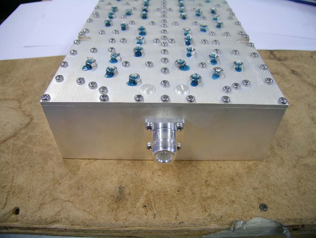
E675JS0118
Jul 26, 2010Nexus Dual Band Repeater
Equipment Class
PCB - PCS Licensed Transmitter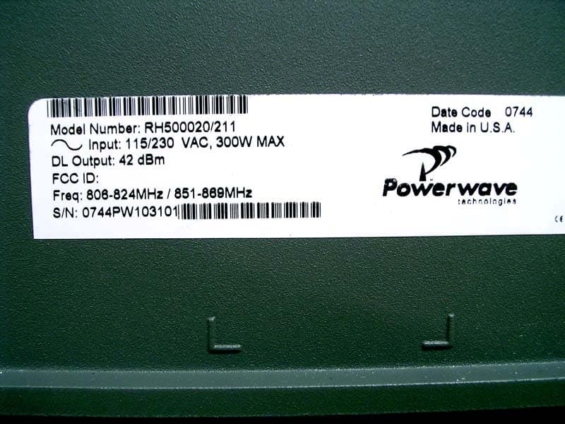
E675JS0096
Jan 10, 2008Wideband Radio Head
Equipment Class
TNB - Licensed Non-Broadcast Station Transmitter