E675JS0064Single-Channel GSM/EDGE Amplifier
Powerwave Technologies Inc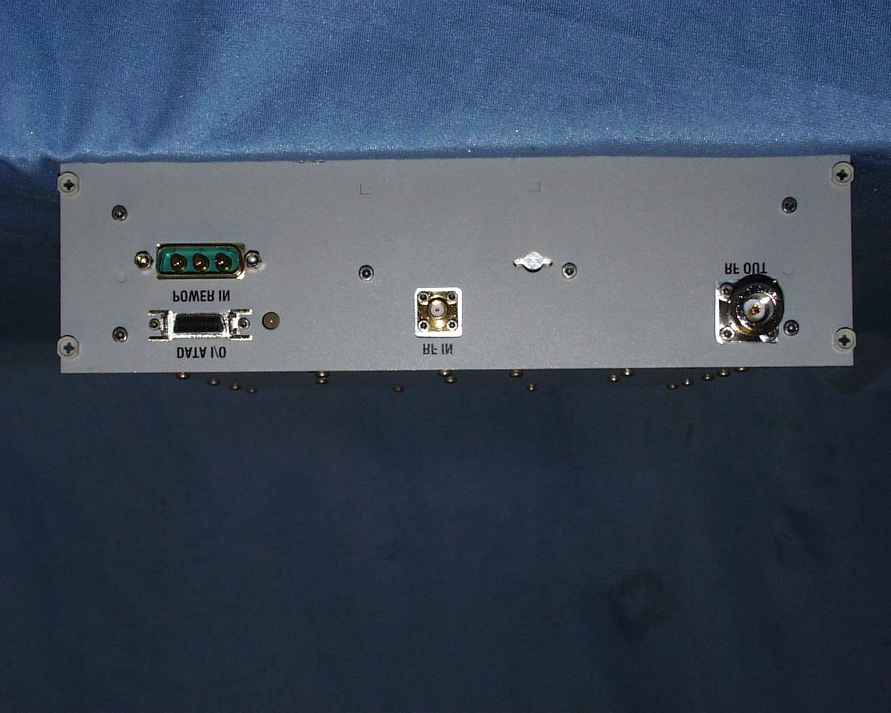
Click to zoom
Application Details
- Equipment Class
- AMP - Amplifier
- Date of Grant
- Apr 08, 2003
- Application Purpose
- Original Equipment
- Date of Application
- Apr 08, 2003
- Equipment Note
- Single-Channel GSM/EDGE Amplifier
- Frequency Range
- 869.00000000 - 894.00000000
- Company
- Powerwave Technologies Inc
- Country
- United States
Documents & Files
Document Text
Text extracted from the exhibit documents filed with the FCC. Open a document above to read the original.
Users Manual
869-894 MHz Copyright Powerwave Technologies, Inc., February 2003. All rights reserved 044-xxxxx Rev.AFebruary 2003 Model SCA 9321-30C Single-Channel Cellular Amplifier Installation & Service Manual SCA 9321-30C Installation & Service Manual Copyright Powerwave Technologies, Inc., February 2003. All rights reserved 044-xxxxx Rev. AiiFebruary 2003 February 2003 Powerwave Technologies, Inc.Tel: (714) 466-1000 1801 East St. Andrew Place(888) 797-9283 Santa Ana, CA 92705Fax: (714) 466-5800 Web Site: www.powerwave.com © 2003 Powerwave Technologies Incorporated. All rights reserved. Powerwave Technologies, and the Powerwave logo are registered trademarks Powerwave Technologies, Inc. reserves the right to make changes to the documentation and equipment, including but not limited to component substitution and circuitry changes. Changes that impact this manual may subsequently be incorporated in a later revision of this manual. SCA 9321-30C Installation & Service Manual Copyright Powerwave Technologies, Inc., February 2003. All rights reserved 044-xxxxx Rev. AFebruary 2003 iii Table Of Contents Par.Section 1Page No.General DescriptionNo. 1-1Introduction.............................................................................................................................1-1 1-2General Description.................................................................................................................1-1 1-3Functional and Physical Specifications....................................................................................1-1 1-4Equipment Changes.................................................................................................................1-1 Section 2 Installation 2-1Introduction.............................................................................................................................2-1 2-2Electrical Service Recommendations.......................................................................................2-1 2-3Unpacking and Inspection.......................................................................................................2-1 2-4Installation Instructions...........................................................................................................2-2 2-5Amplifier Module Connectors..................................................................................................2-2 2-5.1Data I/O Connector.................................................................................................................2-3 2-5.2Amplifier RF Connectors.........................................................................................................2-4 2-5.3DC Power Connector...............................................................................................................2-4 Section 3 Operating Instructions 3-1Introduction.............................................................................................................................3-1 3-2Location and Function of Amplifier Indicators.........................................................................3-1 3-3Initial Start-Up and Operating Procedures...............................................................................3-1 Section 4 Principles of Operation 4-1Introduction.............................................................................................................................4-1 4-2RF Input Signal.......................................................................................................................4-1 4-3RF Output Load.......................................................................................................................4-1 4-4SCA 9321-30C Amplifier........................................................................................................4-1 4-4.1Driver Amplifier......................................................................................................................4-2 4-4.2Main Amplifier.......................................................................................................................4-2 4-4.3Power Distribution...................................................................................................................4-2 4-4.4Multifunction Board................................................................................................................4-2 Section 5 Maintenance 5-1Periodic Maintenance..............................................................................................................5-1 SCA 9321-30C Installation & Service Manual Copyright Powerwave Technologies, Inc., February 2003. All rights reserved 044-xxxxx Rev. AFebruary 2003 iv Section 6 Troubleshooting 6-1Introduction.............................................................................................................................6-1 6-2Trouble shooting......................................................................................................................6-1 6-3Return for Service Procedures..................................................................................................6-1 6-3.1Obtaining an RMA..................................................................................................................6-1 6-3.2Repackaging for Shipment.......................................................................................................6-1 List Of Illustrations FigurePage No.No. 1-1SCA 9321-30C Amplifier........................................................................................................1-3 2-1SCA 9321-30C Front Panel View............................................................................................2-2 2-2Data I/O Connector.................................................................................................................2-3 2-3DC Power Connector.......................................................................................................…
Text truncated - open the document above for the full version.
Cover Letter(s)
From: Claire Hoque Sent: Tuesday, April 08, 2003 1:39 PM To: Mike Kuo Cc: Anne Liang Subject: Powerwave Technologies Inc., FCC ID:E675JS0064, AN03T2734(03U1803) Hi Mike, Here are the answers from Powerwave. Question #1: There are so many duplicated internal photos. Please review the internal photos file submitted. Delete any duplicated photos and also provide additional photo to show the solder side of PCB. ANSWER: Pls see the revised attachment. Powerwave also Powerwave requested additional confidentiality for all the internal photos. Pls see client's comments as belows. I also attached revised confidentiality letter. Please note SGA and SCA uses the same boards. Powerwave Comments: We would like to proceed with requesting confidentiality for the internal photos. I have highlighted in the document you provided the section I believe applies. In four of the attached photos (photos with single model nos.) we are using a process that is not known to the general public/industry. We prefer not to make this publicly available. We feel our product falls into the category stated below. It is sold to only one customer and is serviceable by Powerwave or a licensee. It is definitely not accessible by the general public. "Another example is when a non-consumer device is not accessible by the general public, such as a device mounted on the top of a large tower (or in a fenced enclosure) that is only serviceable by the licensee or his designated technicians." Question #2: Page 12 of test report contains the measurement result of output power. However, there is no unit of measurement indicated on the tabular data. Please make necessary correction. ANSWER: Pls see the revised report. Thanks, Claire
ID Label/Location Info
POWERWAVE TECHNOLOGIES INCORPORATED CANADA: FCC ID: E675JS0064XX E 1 7 8 9 7 52868C-SCA9321
Operational Description
SCA 9321-30C Installation & Service Manual Copyright Powerwave Technologies, Inc., February 2003. All rights reserved 044-05113 Rev.A4-1February 2003 Section 4 Principles of Operation 4-1 Introduction This section contains a functional description of the single-carrier SCA 9321-30C amplifier. 4-2 RF Input Signal The maximum input power should not exceed the levels to produce the maximum rated RF out- put power in table 1-1. This level is approximately 0 dBm, but should be set through the base- transceiver station’s software interface. See the BTS manual for detailed instructions. 4-3 RF Output Load The load impedance should be as good as possible (1.5:1 or better) in the working band for good power transfer to the load. 4-4 SCA 9321-30C Amplifier The amplifier, figure 4-1, has an average output power of 30 watts, and is designed to support transmission in GMSK and EDGE modulation. With an input signal of approximately 0 dBm, the amplifier will operate at its rated output power. The amplifier is comprised of: Driver Amplifier Main Amplifier Multifunction Board DC/DC Converter Module Main Amp Temp Sense Det Driver DAC MCU RS-485 Intfc 20-pin SCSI 3 PWR Conn Red/ Grn Input Filter/ Protection Current Sense DC/DC -48/+26 5 V Reg. Power Supply +26 Multifunction Figure 4-1 SCA 9321-30C Amplifier Block Diagram SCA 9321-30C Installation & Service Manual Copyright Powerwave Technologies, Inc., February 2003. All rights reserved 044-05113 Rev.A4-2February 2003 4-4.1 Driver Amplifier The driver amplifier is a two-stage amplifier which provides approximately 28 dB of gain in the 25 MHz frequency band from 869 to 894 MHz. The amplifier is mounted directly on a heat sink, which is temperature monitored by a thermal sensor. 4-4.2 Main Amplifier The main amplifier is a single-stage Class AB amplifier with approximately 13 dB gain and a P1dB of +50 dBm. The amplifier’s output is protected from output mismatches. The amplifier is designed to meet spectral mask requirements for GSM and EDGE signals when operated up to +45.2 dBm. The amplifier is mounted directly on a heat sink. 4-4.3 Power Distribution The amplifier module operates on a –48 VDC nominal power supply consuming 2.9 amps (typi- cally) current at full power. A DC/DC converter to supply internal circuitry with +26 VDC and +5 VDC. 4-4.4 Multifunction Board The multifunction board enables communication between the amplifier and the base-transceiver station in which it is installed, and stores information about the amplifier. It includes gain control and two gain stages providing 7 dB gain. The multifunction board also monitors several ampli- fier performance parameters and reports output power so that the BTS can maintain the output power within specified limits. When these parameters are beyond acceptable levels, the ampli- fier will alarm. The multifunction board is mounted directly on a heat sink, which is temperature monitored by a thermal sensor. The alarms are: Temperature Alarm - If the internal temperature reaches 90°C, the PA shuts down and communicates an alarm through the digital interface. DC/DC Alarm - If the output voltage of the converter falls below 23.5V, the PA shuts down and communicates an alarm through the digital interface. Over-current Alarm - If the output current of the DC/DC converter goes above a nominal threshold (7.5 A), the PA shuts down and communicates an alarm through the digital interface. Communication Alarm - If the serial interface detects an error in transmission (parity, over- run, framing), an alarm is sent for one burst only during the very next burst. The PA operation is not affected.
Parts List/Tune Up Info
SCA 9321-30C Installation & Service Manual Copyright Powerwave Technologies, Inc., February 2003. All rights reserved 044-xxxxx Rev. A3-1February 2003 Section 3 Operating Instructions 3-1 Introduction This section contains operating instructions for the single channel cellular amplifier system. 3-2 Location And Function Of Amplifier Indicators The front panel LED is located to the right of the 20-pin Data connector and indicates the ampli- fier status. • Green means the amplifier is operating properly. • Red indicates an alarm or off condition. The nature of the alarm can only be determined through the software interface of the Base- Transceiver System (BTS). Please consult the BTS manual for details on monitoring amplifier status. Figure 3-1 Front Panel Indicators 3-3 Initial Start-Up And Operating Procedures To perform the initial start-up, proceed as follows: 1. Verify that all input and output cables are properly connected. CAUTION Before applying power, make sure that the input and output of the amplifier are properly terminated at 50 ohms. Do not operate the amplifier without a load attached. Refer to table 1-1 for input power requirements. Excessive input power may damage the amplifier NOTE The output coaxial cable between the amplifier and the antenna must be 50 ohm coaxial cable. Use of any other cable will distort the output. 2. Turn on supply that provides -48 Vdc to the amplifier system. Do not apply an RF signal to the amplifier system 3. Verify that the LED is lit and the color Green. 4. Turn on external exciter/transceiver and apply RF input signals. Adjust the input power to achieve the desired output power. Refer to the BTS manual for instructions on performing this step. Front Panel Status Indicator
Test Report
FCC CFR47 PART 22 CERTIFICATION TEST REPORT FOR 869-894MHz SINGLE-CHANNEL GSM/EDGE AMPLIFIER MODEL: SCA9321-30C FCC ID: E675JS0064 REPORT NUMBER: 03U1803-1 ISSUE DATE: MARCH 11, 2003 Prepared for POWERWAVE TECHNOLOGIES, INC. 1801 E. St. ANDREW PLACE SANTA ANA, CA 92705 USA Prepared by COMPLIANCE CERTIFICATION SERVICES, INC. 561 F MONTEREY ROAD MORGAN HILL, CA 95037 USA TEL: 408-463-0885 FAX: 408-463-0888 REPORT NO: 03U1803-1 DATE: MARCH 11, 2003 FCC ID: E675JS0064 EUT: 869-894MHz GSM / EDGE SINGLE-CHANNEL AMPLIFIER PAGE 2 OF 64 COMPLIANCE CERTIFICATION SERVICES DOCUMENT NO:CCSUP4031A 561 F MONTEREY ROAD, MORGAN HILL, CA 95037 USA TEL:(408) 463-0885 FAX:(408) 463-0888 This report shall not be reproduced except in full, without the written approval of CCS. This document may be altered or revised by Compliance Certification Services personnel only, and shall be noted in the revision section of the document. TABLE OF CONTENTS PAGE 1. FCC CERTIFICATION INFORMATION....................................................................................................3 2. TEST FACILITY..............................................................................................................................................4 3. ACCREDITATION AND LISTING...............................................................................................................4 4. MEASUREMENT INSTRUMENTATION....................................................................................................4 5. MEASURING INSTRUMENT CALIBRATION...........................................................................................4 6. UNITS OF MEASUREMENT.........................................................................................................................5 7. EQUIPMENT MODIFICATIONS..................................................................................................................5 8. TEST EQUIPMENT LIST................................................................................................................................6 9. EUT SETUP PHOTOS.....................................................................................................................................7 10. EXTERNAL I/O CABLE CONSTRUCTION DESCRIPTION.................................................................10 11. CONFIGURATION BLOCK DIAGRAM....................................................................................................10 12. PART 2: CERTIFICATION TEST REQUIREMENT:.............................................................................11 SECTION 2.1046: RF POWER OUTPUT............................................................................................................11 SECTION 2.1047: MODULATION CHARACTERISTICS.................................................................................13 SECTION 2.1049: OCCUPIED BANDWIDTH...................................................................................................13 SECTION 2.1051: SPURIOUS EMISSION AT ANTENNA TERMINALS........................................................21 SECTION 2.1055: FREQUENCY STABILITY...................................................................................................32 RADIATED EMISSIONS.....................................................................................................................................32 ATTACHMENTS.....................................................................................................................................................38 EUT PHOTOGRAPHS............................................................................................................................................39 REPORT NO: 03U1803-1 DATE: MARCH 11, 2003 FCC ID: E675JS0064 EUT: 869-894MHz GSM / EDGE SINGLE-CHANNEL AMPLIFIER Page 3 of 45 COMPLIANCE CERTIFICATION SERVICES DOCUMENT NO:CCSUP4031A 561 F MONTEREY ROAD, MORGAN HILL, CA 95037 USA TEL:(408) 463-0885 FAX:(408) 463-0888 This report shall not be reproduced except in full, without the written approval of CCS. This document may be altered or revised by Compliance Certification Services personnel only, and shall be noted in the revision section of the document. 1. FCC CERTIFICATION INFORMATION The following information is in accordance with FCC Rules, 47CFR Part2, Subpart J, Sections 2.1033 – 2.1055. 2.1033(c)(1) Applicant: POWERWAVE TECHNOLOGIES, INC. 1801 E. St. ANDREW PLACE SANTA ANA, CA 92705 Contact person: CLINT LAWRENCE Telephone number: (916) 941-3167 2.1033(c)(2) FCC ID: E675JS0064 2.1033(c)(4) Types of Emissions: G7W (EDGE), GXW (GSM) 2.1033(c)(5) Frequency Range: 869 – 894 MHz 2.1033(c)(6) Range of Operation Power: 30Watts 2.1033(c)(7) Maximum Power Rating: 30 Watts 2.1033(c)(8) DC Voltage and DC Current: -48Vdc @ 2.9 A; typical Section 22.913(a); Maximum ERP. The effective radiated power (ERP) of base transmitters and cellular repeaters must not exceed 500 Watts. TYPE OF EQUIPMENT: CELLULAR AMPLIFIER MEASUREMENT DISTANCE: 3 METER TECHNICAL LIMIT: FCC 22.359, 22.917 FCC RULES: PART 22 EQUIPMENT AUTHORIZATION PROCEDURE CERTIFICATION / PERMISSIVE CHANGE MODIFICATIONS MADE ON EUT YES (REFER TO PAGE 5) NO The above equipment was tested by Compliance Certification Services for compliance with the requirements set forth in the FCC CFR 47, PART 22. The results of testing in this report apply to the product/system, which was tested only. Other similar equipment will not necessarily produce the same results due to production tolerance and measurement uncertainties. TESTED BY: REVIEWED and RELEASED BY: VIEN TRAN THU CHAN ASSOCIATE EMC ENGINEER EMC SUPERVISOR COMPLIANCE CERTIFICATION SERVICES COMPLIANCE CERTIFICATION SERVICES REPORT NO: 03U1803-1 DATE: MARCH 11, 2003 FCC ID: E675JS0064 EUT: 869-894MHz GSM / EDGE SINGLE-CHANNEL AMPLIFIER Page 4 of 45 COMPLIANCE CERTIFICATION SERVICES DOCUMENT NO:CCSUP4031A 561 F MONTEREY ROAD, MORGAN HILL, CA 95037 USA TEL:(408) 463-0885 FAX:(408) 463-08…
Text truncated - open the document above for the full version.
Test Setup Photos
REPORT NO: 03U1803-1 DATE: MARCH 11, 2003 FCC ID: E675JS0064 EUT: 869-894MHz GSM / EDGE SINGLE-CHANNEL AMPLIFIER Page 7 of 45 COMPLIANCE CERTIFICATION SERVICES DOCUMENT NO:CCSUP4031A 561 F MONTEREY ROAD, MORGAN HILL, CA 95037 USA TEL:(408) 463-0885 FAX:(408) 463-0888 This report shall not be reproduced except in full, without the written approval of CCS. This document may be altered or revised by Compliance Certification Services personnel only, and shall be noted in the revision section of the document. 9. EUT SETUP PHOTOS Occupied Bandwidth Input Setup REPORT NO: 03U1803-1 DATE: MARCH 11, 2003 FCC ID: E675JS0064 EUT: 869-894MHz GSM / EDGE SINGLE-CHANNEL AMPLIFIER Page 8 of 45 COMPLIANCE CERTIFICATION SERVICES DOCUMENT NO:CCSUP4031A 561 F MONTEREY ROAD, MORGAN HILL, CA 95037 USA TEL:(408) 463-0885 FAX:(408) 463-0888 This report shall not be reproduced except in full, without the written approval of CCS. This document may be altered or revised by Compliance Certification Services personnel only, and shall be noted in the revision section of the document. Occupied Bandwidth Output Setup REPORT NO: 03U1803-1 DATE: MARCH 11, 2003 FCC ID: E675JS0064 EUT: 869-894MHz GSM / EDGE SINGLE-CHANNEL AMPLIFIER Page 9 of 45 COMPLIANCE CERTIFICATION SERVICES DOCUMENT NO:CCSUP4031A 561 F MONTEREY ROAD, MORGAN HILL, CA 95037 USA TEL:(408) 463-0885 FAX:(408) 463-0888 This report shall not be reproduced except in full, without the written approval of CCS. This document may be altered or revised by Compliance Certification Services personnel only, and shall be noted in the revision section of the document. Radiated Emission Setup
Contact Information
Applicant
Jeff Dale(Principal Reliability Engineer)
Test Firm
Compliance Certification Services IncSteve Cheng
Technical Specifications
| # | Rule Parts | Frequency Range | Power Output | Emission | Tolerance |
|---|---|---|---|---|---|
| 2 | 22.901(d) | 869 MHz - 894 MHz | 30 W | G7W | Amp |
Other Applications from Powerwave Technologies Inc
E675JS0123
Nov 03, 2011Multi-carrier RF Power Amplifier
Equipment Class
AMP - Amplifier
E675JS0120
Aug 26, 2010Nexus Dual Band Repeater
Equipment Class
TNB - Licensed Non-Broadcast Station Transmitter
E675JS0119
Aug 01, 2010Nexus Dual Band Repeater
Equipment Class
PCB - PCS Licensed Transmitter
E675JS0118
Jul 26, 2010Nexus Dual Band Repeater
Equipment Class
PCB - PCS Licensed Transmitter
E675JS0096
Jan 10, 2008Wideband Radio Head
Equipment Class
TNB - Licensed Non-Broadcast Station Transmitter