E675JS0067W-CDMA Multi-Channel PCS Amplifier
Powerwave Technologies Inc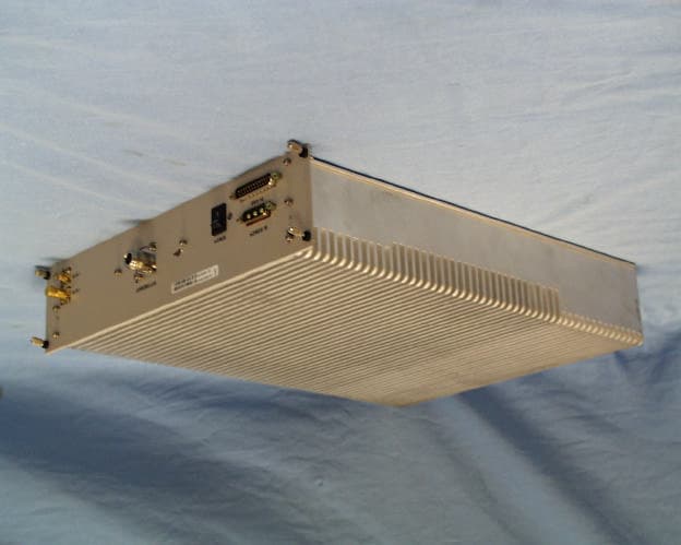
Click to zoom
Application Details
- Equipment Class
- AMP - Amplifier
- Date of Grant
- Jun 26, 2003
- Application Purpose
- Original Equipment
- Date of Application
- Jun 26, 2003
- Equipment Note
- W-CDMA Multi-Channel PCS Amplifier
- Frequency Range
- 1930.00000000 - 1990.00000000
- Company
- Powerwave Technologies Inc
- Country
- United States
Documents & Files
Document Text
Text extracted from the exhibit documents filed with the FCC. Open a document above to read the original.
Users Manual
1930-1990 MHz Installation & Service Manual Model NTUM30DA Multi-Channel PCS Amplifier Copyright Powerwave Technologies, Inc., June 2003. All rights reserved 044-05141 Rev. A June 2003 NTUM30DA Installation & Service Manual Copyright Powerwave Technologies, Inc., June 2003. All rights reserved June 2003 © 2003 Powerwave Technologies Incorporated. All rights reserved. Powerwave Technologies, and the Powerwave logo are registered trademarks Powerwave Technologies, Inc. reserves the right to make changes to the documentation and equipment, including but not limited to component substitution and circuitry changes. Changes that impact this manual may subsequently be incorporated in a later revision of this manual. Powerwave Technologies, Inc. Tel: (714) 466-1000 1801 East St. Andrew Place (888) 797-9283 Santa Ana, CA 92705 Fax: (714) 466-5800 Web Site: www.powerwave.com 044-05141 Rev. A ii June 2003 NTUM30DA Installation & Service Manual Table Of Contents Par. Section 1 Page No. General Description No. 1-1 Introduction.....................................................................................................................................................1-1 1-2 General Description.......................................................................................................................................1-1 1-3 Functional and Physical Specifications....................................................................................................1-1 Section 2 Installation 2-1 Introduction.....................................................................................................................................................2-1 2-2 Electrical Service Recommendations........................................................................................................2-1 2-3 Unpacking and Inspection............................................................................................................................2-1 2-4 Installation Instructions................................................................................................................................2-2 2-5 Power In Connector.......................................................................................................................................2-2 2-6 Data I/O Connector.........................................................................................................................................2-3 2-7 P3: Differential IIC Clock, Receive, & Transmit Connector................................................................... 2-4 2-8 P4: IIC, Power, Alarms, & Controls Connector.........................................................................................2-4 2-9 P5: IIC, RS485, Power, & Other Signals Connector.................................................................................2-6 Section 3 Operating Instructions 3-1 Introduction.....................................................................................................................................................3-1 3-2 Initial Start-Up and Operating Procedures...............................................................................................3-1 Section 4 Principles of Operation 4-1 Introduction.....................................................................................................................................................4-1 4-2 RF Input Signal................................................................................................................................................4-1 4-3 RF Output Load................................................................................................................................................4-1 4-4 Amplifier Functional Description................................................................................................................4-1 4-4.1 Input Amplifier................................................................................................................................................4-1 4-4.2 1 st Loop Phase & Gain....................................................................................................................................4-1 4-4.3 Driver Amplifier..............................................................................................................................................4-2 4-4.4 Main Amplifier................................................................................................................................................4-2 4-4.5 Multifunction Board.......................................................................................................................................4-2 4-5 Amplifier Module Cooling............................................................................................................................4-2 4-6 Power Distribution.........................................................................................................................................4-3 4-7 Amplifier Alarms.............................................................................................................................................4-3 4-7.1 Minor Alarms...................................................................................................................................................4-3 4-7.1.1 Main Loop Cancellation Alarm (1 st Loop Alarm)......................................................................................4-3 4-7.1.2 Error Loop Cancellation Alarm (2 nd Loop Alarm)......................................................................................4-4 4-7.1.3 Gain Alarm.......................................................................................................................................................4-4 4-7.1.4 Partial Failure of Main Amplifier Alarm (Transistor/Device Fail)........................................................4-4 4-…
Text truncated - open the document above for the full version.
Cover Letter(s)
From: Helen Zhao Sent: Friday, June 27, 2003 4:41 PM To: Mike Kuo Cc: Anne Liang; Steve Cheng; Sylvia Lin Subject: RE: Powerwave Technologies Inc. FCC ID:E675JS0067, AN03T2947 Hello Mike, Question #1: Please provide justification for requesting internal photos as confidential document. Answer: <Powerwave Comments> We would like to proceed with requesting confidentiality for the internal photos. I have highlighted in the document you provided the section I believe applies. In four of the attached photos (photos with single model nos.) we are using a process that is not known to the general public/industry. We prefer not to make this publicly available. We feel our product falls into the category stated below. It is sold to only one customer and is serviceable by Powerwave or a licensee. It is definitely not accessible by the general public. "Another example is when a non-consumer device is not accessible by the general public, such as a device mounted on the top of a large tower (or in a fenced enclosure) that is only serviceable by the licensee or his designated technicians." Thank you! Helen
External Photos
External Photos Front Side Rear Side
ID Label/Location Info
POWERWAVE TECHNOLOGIES INCORPORATED CANADA: FCC ID: E675JS0067 XX E 1 7 8 9 7 5 2868C-NTUM30DA
Operational Description
NTUM30DA Installation & Service Manual Section 4 Principles of Operation 4-1 Introduction This section contains a functional description of the multichannel power amplifier (MCPA). 4-2 RF Input Signal The maximum input power should not exceed the limits specified in table 1-1. 4-3 RF Output Load The load impedance should be as good as possible (1.5:1 or better) in the working band for good power transfer to the load. 4-4 Amplifier Functional Description The NTUM30DA amplifier (figures 1-1 and 4-1) is a linear, MCPA that operates in the 60 MHz frequency band from 1930 MHz to 1990 MHz with an instantaneous bandwidth of 20 MHz. The operating band is determined by the operating frequency selection(s) of the base station (refer to table 1-1). The amplifier produces 45 watts of output power when operated in mode 1 or 30 watts of output power when operated in mode 2. Each amplifier is a self-contained module and is func- tionally independent of any other amplifier module(s) in the system. Each amplifier module has an alarm board that monitors the amplifier performance. If a failure or fault occurs in an amplifier module, it is transmitted to the host system via an RS-485 interface. The amplifier is compliant to the requirements of FCC rules with respect to spurious emissions (see table 1-1). Constant gain is maintained by continuously comparing active paths with passive references, and correcting for small variations through the RF feedback controls. All gain varia- tions, for example those due to temperature, are reduced to the passive reference variations. The amplifier module is comprised of: An input amplifier 1 st Loop Phase & Gain A driver amplifier A main amplifier A multifunction board 4-4.1 Input Amplifier RF is fed to the input amplifier, which consists of an isolator at the input, bandpass filter, voltage variable attenuators (VVA), and phase shifters for gain control and phase sweeping functions. The circuits in this section of the amplifier are controlled by a microprocessor on the Multifunction board. At its output, the input amplifier splits the signal to the 1 st Loop Phase and Gain circuit, and the carrier cancellation circuit. 4-4.2 1 st Loop Phase & Gain The 1 st Loop Phase & Gain circuit is a predistortion amplifier. The input signal is predistorted such that it linearizes the output of the main amp at the rated output power of the MCPA. It also contains the main loop VVAs and phase shifters. All the predistortion voltages and loop voltages are controlled by a microprocessor. Copyright Powerwave Technologies, Inc., June 2003. All rights reserved 044-05141 Rev. A 4-1 June 2003 NTUM30DA Installation & Service Manual 4-4.3 Driver Amplifier The driver amplifier consists of two stages of class AB amplification, which provide the approxi- mately 40% of the gain in the 60 MHz frequency band from 1930 MHz to 1990 MHz. 4-4.4 Main Amplifier The main amplifier employs two class AB amplification stages for maximum efficiency. It provides approximately 40% of the gain in the 60 MHz frequency band. The output from the main amplifier is typically higher than the rated output power of the MCPA, to allow for losses associated with the components in the remaining RF path. The RF signals are then applied to a delay line and directional coupler, where the distortion products are cancelled out and the amplifier power per- formance is monitored. 4-4.5 Multifunction Board The multifunction board consists of feed forward loop control and alarm circuits. The MCPA com- municates to the host system through the multifunction board, which gathers the status informa- tion of the amplifier and reports to the host system via the RS-485 interface when instructed. It also protects the MCPA from adverse conditions such as overpower, input overdrive, over- voltage, etc. A microprocessor on the multifunction board also controls two loops in the feed- forward system. Pre Amp Driver Main Amp Error Amp Delay Feed Forward Loop control 2nd Loop Phase & Gain 1st Loop Phase & Gain Delay Alarms & Display +15 +5 -5 Power Supply -30dB -10dB -40dB RF Out RFL PWR FWD PWR Front Panel Smart Rack +27VDC Figure 4-1 NTUM30DA Multichannel Power Amplifier Functional Block Diagram 4-5 Amplifier Module Cooling Each amplifier module is contained within a thermally conductive chassis and properly mounted on an adequate thermal surface, which provides sufficient cooling when forced air is circulated over the heat sink fins to maintain the amplifier within the specified operating temperature range. Copyright Powerwave Technologies, Inc., June 2003. All rights reserved 044-05141 Rev. A 4-2 June 2003 NTUM30DA Installation & Service Manual 4-6 Power Distribution Primary DC power for the amplifier is provided by the host system. The amplifier generates all the required voltages internally from the main source. 4-7 Amplifier Alarms 4-7.1 Minor Alarms When a minor alarm condition occurs, the alarm is latched into a minor alarm condition. The am- plifier alarm state is read by the BTS the next time the amplifier is poled by the BTS. After the alarm status is sent the minor alarm register is cleared, unless the alarm condition still exists. If the amplifier receives a “Enable Command” or “Clear Alarms Command”, all minor alarms will be cleared. If the amplifier is disabled, all minor alarms are also cleared. Minor alarms do not directly affect amplifier functionality. BTS MCPA OPERATIONAL Read Power and Status response - Alarm reported Minor Alarm condition appears Minor Alarm condition disappears Read Power and Status command Minor Alarm condition still exists Read Power and Status command Read Power and Status response - Alarm reported Read Power and Status command Read Power and Status response - No Alarm reported Figure 4-2 Minor Alarm Reporting Sequence 4-7.1.1 Main Loop Cancellation Alarm (1 st Loop Alarm) During normal operation, if the 1 st Loop is not locked for 30 seconds a Main Loop Cancellation Alarm is declared. During power-u…
Text truncated - open the document above for the full version.
Parts List/Tune Up Info
NTUM30DA Installation & Service Manual Section 3 Operating Instructions 3-1 Introduction This section contains operating instructions for the Multicarrier Cellular Amplifier. 3-2 Initial Start-Up & Operating Procedures There are no operating controls or indicators on the NTUM30DA amplifier module. To perform the initial start-up, proceed as follows: 1. Verify that all input and output cables are properly connected, per section 2. CAUTION Before applying power, make sure that the input and output of the amplifier are prop- erly terminated at 50 ohms. Do not operate the amplifier without a load attached. Re- fer to table 1-1 for input power requirements. Excessive input power may damage the amplifier. NOTE The output coaxial cable between the amplifier and the antenna must be 50 ohm co- axial cable. Use of any other cable will distort the output. 2. Turn on supply that provides -48 Vdc to the amplifier system. 3. Turn the amplifier front panel switch to On. The amplifier will run through built-in-test for a few seconds, and notify the BTS when the loops converge. The base station allows up to 30 seconds for this step to complete. 4. Turn on external exciter/transceiver and apply RF input signals. Copyright Powerwave Technologies, Inc., June 2003. All rights reserved 044-05141 Rev. A 3-1 June 2003
Test Report
FCC CFR47 PART 24 SUBPART E BROADBAND CERTIFICATION REPORT FOR 1930-1990MHz W-CDMA MULTI-CARRIER POWER AMPLIFIER (45W) MODEL: NTUM30DA FCC ID: E675JS0067 REPORT NUMBER: 03U1998-1 ISSUE DATE: 06/06/03 Prepared for POWERWAVE TECHNOLOGIES, INC. 1117 WINDFIELD WAY, SUITE 100 EL DORADO HILLS, CA 95762 Prepared by COMPLIANCE CERTIFICATION SERVICES 561F Monterey Road Morgan Hill, CA 95037 U.S.A. TEL: (408) 463-0885 FAX: (408) 463-0888 PROJECT NO: 03U1998-1 FCC ID: E675JS0067 DATE: JUNE 06, 2003 EUT: 1930-1990MHz W-CDMA MULTI-CRRIER POWER AMPLIFIER (45W) PAGE 2 OF 32 COMPLIANCE CERTIFICATION SERVICES DOCUMENT NO:CCSUP4031A 561F Monterey Rd., Morgan Hill, CA 95037-9001, USA TEL:(408) 752-8166 FAX:(408) 752-8168 This report shall not be reproduced except in full, without the written approval of CCS. TABLE OF CONTENT 1. TEST RESULT CERTIFICATION.....................................................................................................................3 2. EUT DESCRIPTION...............................................................................................................................................4 3. FACILITIES, LABORATORY AND ACCREDITATION..........................................................................4 3.1. FACILITIES.........................................................................................................................................................4 3.2. LABORATORY ACCREDITATION.............................................................................................................4 3.3. LIST OF ACCREDITATIONS.........................................................................................................................5 4. CALIBRATION, METHODOLOGY AND UNCERTAINTY....................................................................6 4.1. EQUIPMENT CALIBRATION........................................................................................................................6 4.2. TEST METHODOLOGY..................................................................................................................................6 4.3. MEASUREMENT UNCERTAINTY..............................................................................................................6 4.4 TEST AND MEASUREMENT EQUIPMENT...............................................................................................7 5. APPLICABLE RULES............................................................................................................................................7 5.1. RF POWER OUTPUT §2.1046........................................................................................................................7 5.2. MODULATION CHARACTERISTICS §2.1047.........................................................................................7 5.3. OCCUPIED BANDWIDTH §2.1049..............................................................................................................8 5.4. SPURIOUS EMISSIONS AT ANTENNA TERMINALS §2.1051...........................................................8 5.5. FIELD STRENGTH OF SPURIOUS RADIATION §2.1053.....................................................................8 5.6. FREQUENCY STABILITY §2.1055..............................................................................................................8 5.7 FREQUENCY RANGE TO BE INVESTIGATED §2.1057........................................................................9 5.8. RADIATED EMISSIONS, FCC PART 15, SECTIONS 209 & 205.......................................................10 6. TEST SETUP, PROCEDURES, AND RESULTS.........................................................................................11 6.1.1 RF CONDUCTED POWER OUTPUT.......................................................................................................11 6.1.2 RF RADIATED POWER OUTPUT............................................................................................................12 6.2. OCCUPIED BANDWIDTH............................................................................................................................13 6.3. SPURIOUS EMISSIONS AT ANTENNA TERMINAL...........................................................................20 6.4 FIELD STRENGTH OF SPURIOUS RADIATION....................................................................................23 6.5. RADIATED EMISSIONS, FCC PART 15, SECTIONS 209 & 205.......................................................27 7. ATTACHMENT.................................................................................................................................................30 7.1 EUT SETUP PHOTOS..............................................................................................................................30 7.2 EUT PHOTOGRAPHS...............................................................................................................................32 7.3 INSTALLATION AND SERVICE MANUAL......................................................................................32 7.4 SCHEMATIC, PART LISTS AND BLOCK DIAGRAM...................................................................32 7.5 PROPOSED FCC ID LABEL FORMAT................................................................................................32 PROJECT NO: 03U1998-1 FCC ID: E675JS0067 DATE: JUNE 06, 2003 EUT: 1930-1990MHz W-CDMA MULTI-CRRIER POWER AMPLIFIER (45W) PAGE 3 OF 32 COMPLIANCE CERTIFICATION SERVICES DOCUMENT NO:CCSUP4031A 561F Monterey Rd., Morgan Hill, CA 95037-9001, USA TEL:(408) 752-8166 FAX:(408) 752-8168 This report shall not be reproduced except in full, without the written approval of CCS. 1. TEST RESULT CERTIFICATION COMPANY NAME: POWERWAVE TECHNOLOGIES, INC. 1117 WINDFIELD WAY, SUITE 100 EL DORADO HILLS, CA 95762 EUT DESCRIPTION: 1930-1990MHz W-CDMA MULTI-CRRIER POWER AMPLIFIER (45W) MODEL NUMBER: NTUM30DA DATE TESTED: MAY 20, 2003 – MAY 25, 2003 EQUIPMENT TYPE INTENTIONAL RADIAT…
Text truncated - open the document above for the full version.
Test Report
Measurement Result Plots 2 1 4 3 6 5 8 7 10 9 12 11 14 13 16 15 18 17 20 19 22 21 24 23 26 25 28 27 30 29 32 31 34 33 36 35 38 37 40 39 42 41
Test Setup Photos
PROJECT NO: 03U1998-1 FCC ID: E675JS0067 DATE: JUNE 06, 2003 EUT: 1930-1990MHz W-CDMA MULTI-CRRIER POWER AMPLIFIER (45W) PAGE 30 OF 32 COMPLIANCE CERTIFICATION SERVICES DOCUMENT NO:CCSUP4031A 561F Monterey Rd., Morgan Hill, CA 95037-9001, USA TEL:(408) 752-8166 FAX:(408) 752-8168 This report shall not be reproduced except in full, without the written approval of CCS. 7. ATTACHMENT 7.1 EUT SETUP PHOTOS CONDUCTED RF MEASUREMENTS HIGH FREQUENCY, VERTICAL POLARIZATION PROJECT NO: 03U1998-1 FCC ID: E675JS0067 DATE: JUNE 06, 2003 EUT: 1930-1990MHz W-CDMA MULTI-CRRIER POWER AMPLIFIER (45W) PAGE 31 OF 32 COMPLIANCE CERTIFICATION SERVICES DOCUMENT NO:CCSUP4031A 561F Monterey Rd., Morgan Hill, CA 95037-9001, USA TEL:(408) 752-8166 FAX:(408) 752-8168 This report shall not be reproduced except in full, without the written approval of CCS. RADIATED EMISSIONS
Contact Information
Applicant
Jeff Dale(Principal Reliability Engineer)
Test Firm
Compliance Certification Services IncSteve Cheng
Technical Specifications
| # | Rule Parts | Frequency Range | Power Output | Emission | Tolerance |
|---|---|---|---|---|---|
| 1 | 24 | 1.93 GHz - 1.99 GHz | 45 W | F9W | Amp |
Other Applications from Powerwave Technologies Inc
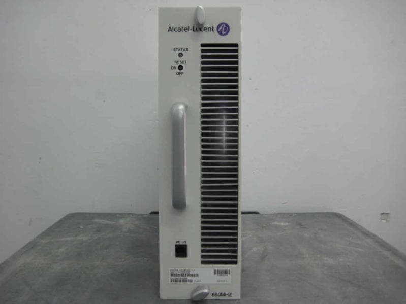
E675JS0123
Nov 03, 2011Multi-carrier RF Power Amplifier
Equipment Class
AMP - Amplifier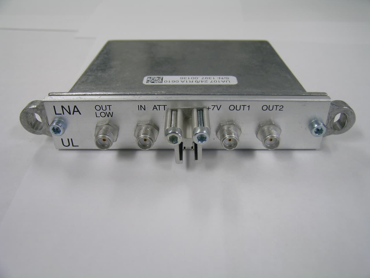
E675JS0120
Aug 26, 2010Nexus Dual Band Repeater
Equipment Class
TNB - Licensed Non-Broadcast Station Transmitter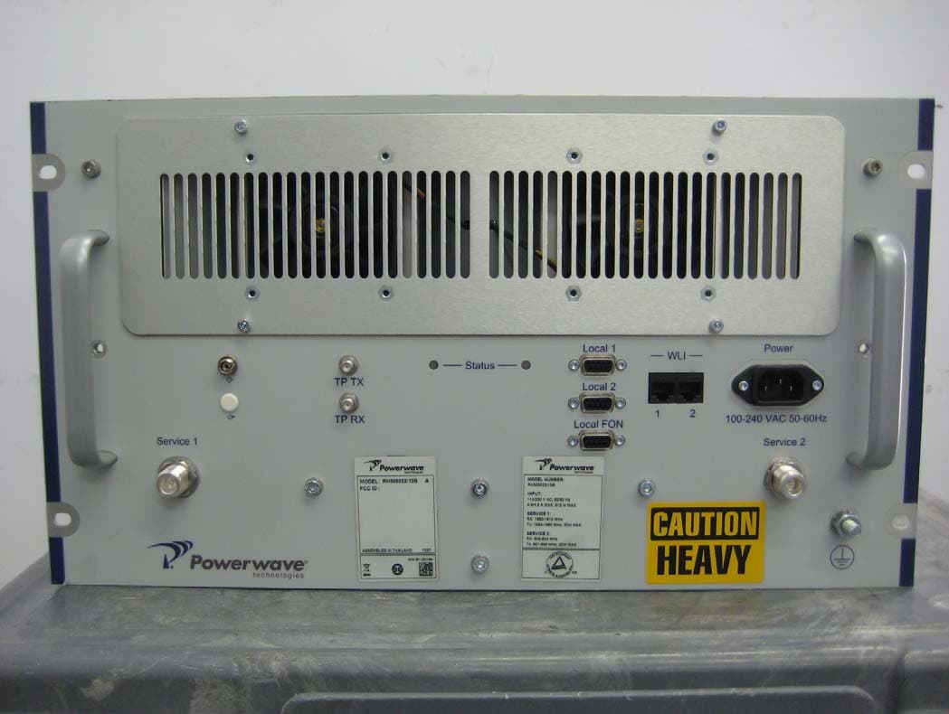
E675JS0119
Aug 01, 2010Nexus Dual Band Repeater
Equipment Class
PCB - PCS Licensed Transmitter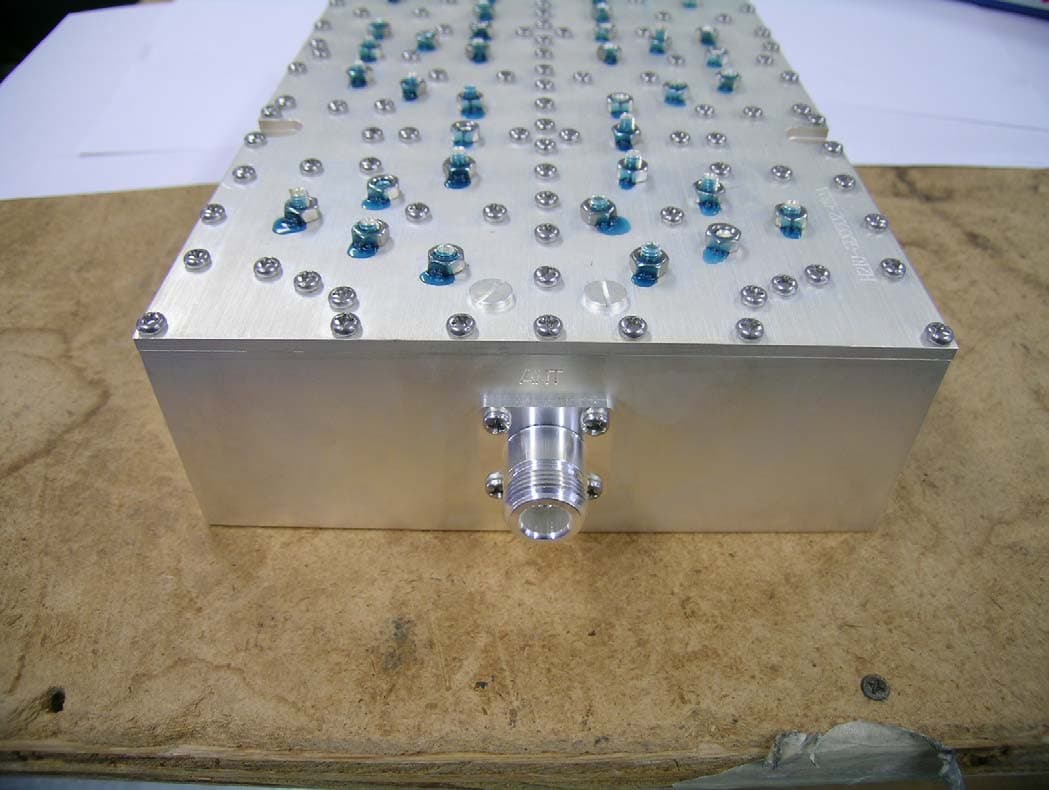
E675JS0118
Jul 26, 2010Nexus Dual Band Repeater
Equipment Class
PCB - PCS Licensed Transmitter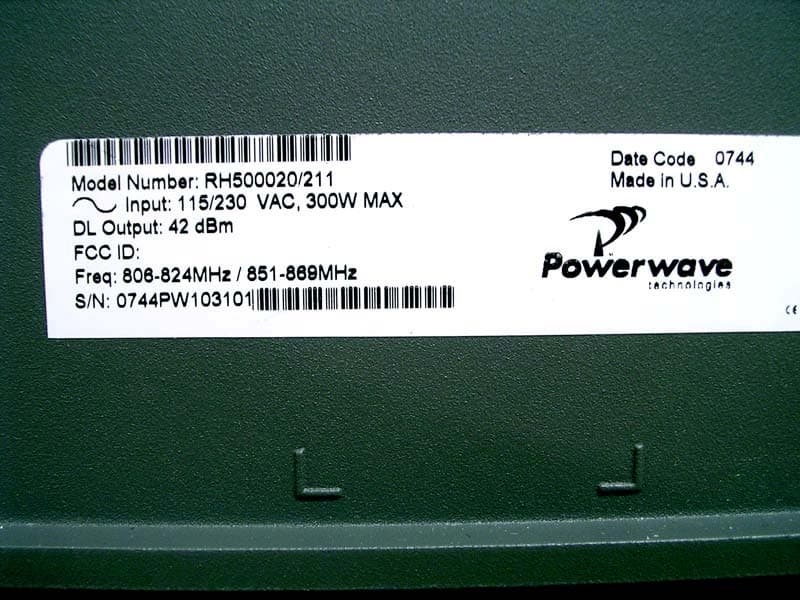
E675JS0096
Jan 10, 2008Wideband Radio Head
Equipment Class
TNB - Licensed Non-Broadcast Station Transmitter