E675JS0070Three Sector 1900 MHz RF Power Amplifier Cabinet
Powerwave Technologies IncApplication Details
- Equipment Class
- AMP - Amplifier
- Date of Grant
- Sep 18, 2004
- Application Purpose
- Original Equipment
- Date of Application
- Sep 18, 2004
- Equipment Note
- Three Sector 1900 MHz RF Power Amplifier Cabinet
- Frequency Range
- 1930.00000000 - 1990.00000000
- Company
- Powerwave Technologies Inc
- Country
- United States
Documents & Files
Document Text
Text extracted from the exhibit documents filed with the FCC. Open a document above to read the original.
Users Manual
044-05156 Rev C 1 Reference Manual 1. Abbreviations and Acronyms Abbreviation / Acronym Definition { = Two definitions, { same abbreviation/acronym ACLR....................................................... Adjacent Channel Leakage Power Ratio ACP......................................................... Adjacent Channel Power A/D .......................................................... Analog-to-Digital Conversion ADC......................................................... {Analog-to-Digital Converter {Automatic Data Collection AM ........................................................... Amplitude Modulation AMPS ...................................................... Advanced Mobile Phone System ANSI........................................................ American National Standards Institute APC......................................................... Automatic Power Control APTT ....................................................... Analog Push To Talk ASG......................................................... Applications Support Group ASIC........................................................ Application Specific Integrated Circuit ATE ......................................................... Automatic (Automated) Test Equipment ATP ......................................................... Acceptance Test Procedure ATTEN .................................................... Attenuator BER......................................................... Beyond Economical Repair BOM ........................................................ Bill Of Materials BPF ......................................................... Band Pass Filter BS ........................................................... Base Station BTS ......................................................... Base Transceiver Station (System) BW .......................................................... BandWidth °C ............................................................ Degrees Celsius CAD......................................................... Computer Aided Design CCA......................................................... {Circuit Card Assembly CCW........................................................ Counter ClockWise CDMA...................................................... Code Division Multiple Access CDPD ......................................................Cellular Digital Packet Data CTRL....................................................... Control CW .......................................................... {ClockWise {Continuous Wave dB ............................................................ deciBels dBc .......................................................... Referenced to a carrier level dBm......................................................... Reference to a specific power level (one milliwatt) dBw ......................................................... Reference to a specific power level (one watt) DIN ......................................................... Deutsches Insitut für Normung eV DLNA....................................................... Duplexer Low Noise Amplifier DPTT....................................................... Digital Push To Talk DQPSK.................................................... Differential Quadrature Phase Shift Keyed DSP......................................................... Digital Signal Processing DUT......................................................... Device Under Test ECD......................................................... Estimated Completion Date ECM ........................................................ Electronic Counter Measure EDGE ...................................................... Enhanced Data for GSM Evolution EEPROM................................................. Electrically-Erasable Programmable Read-Only Memory EIA .......................................................... Electronic Industries Association EMC ........................................................ ElectroMagnetic Compatibility EMI .......................................................... ElectroMagnetic Interference EPROM ................................................... {Electrically Programmable Read-Only Memory {Erasable Programmable Read-Only Memory 044-05156 Rev C 2 ESD......................................................... ElectroStatic Discharge ESG......................................................... Electronic Signal Generator ETDMA.................................................... Extended Time Division Multiple Access ETSI ........................................................ European Telecommunications Standard Institute EUT ......................................................... Equipment Under Test FAR ......................................................... Failure Analysis Report FCC......................................................... Federal Communications Commission FDMA ...................................................... Frequency Division Multiple Access FET ......................................................... Field Effect Transistor FHMA ...................................................... Frequency Hopping Multiple Access FM ........................................................... Frequency Modulation FRU......................................................... Field Replaceable Unit FSK ......................................................... Frequency Shift Key modulation GHz ......................................................... GigaHertz GMSK...................................................... Gaussian Minimum Shift Keying GOLAY.................................................... See GSC GSC ........................................................ Golay Sequential Code GSM ........................................................ Global System for Mobile Communications HPF ......................................................... High Pass Filter HW .......................…
Text truncated - open the document above for the full version.
Block Diagram
LVD Monitor System Interface Module 150 A Main CB 4 KW (148 amp) Rectifier Line Line GND 4 KW (148 amp) Rectifier Line Line GND 4 KW (148 amp) Rectifier Line Line GND 4 KW (148 amp) Rectifier Line Line GND 4 KW (148 amp) Rectifier Line Line GND Alpha Amplifier Subrack Beta Amplifier Subrack Gamma Amplifier Subrack Alarm 1Alarm 2Alarm 3 04-0063B-B DLNA 3 DLNA 2 DLNA 1 DLNA 0 DLNA 4 DLNA 5 30 A CB 30 A CB 30 A CB 30 A CB 30 A CB 15 A CB GFCI Outlet 15 A CB AC Relay 20 A CB Surge Pro. 30 A CB Battery Heater 30 A CB Reserved Line Line 100 A 100 A T EMI Filter Line Line GND Bus Neutral Bus GND Neu Connect when wired as Main Panel; Disconnect when wired as Sub-Panel (default) Customer Supplied Prewired Prewired 600A600A K1 K1K2K3 K4 600A
Block Diagram
Pre Amp Pre Main Main Amp Error Amp Delay Feed Forward Loop control 2nd Loop Phase & Gain 1st Loop Phase & Gain Delay Alarms & Display +15 +5 -5 Power Supply RF Out RFL PWR FWD PWR Front Panel Smart Rack +27VDC Pre Dist Phase & Gain
Block Diagram
System Interface Module AFE D B C I 2 C d I 2 C m 1 3 2 FORM-C 6 66 9 99 99 9 MCR21929-1-2 Max Combined Power 220W (53.4dBm) +51.5 +/-0.5dB Gain Max 10 dB Dynamic Range VVA Controller G3S-1900-125 Switch Comb. S p l i t t e r +27VDC GND Form-C 1 6 To Controller RS-485 RS-485 VVA_Contro l Switch_ Control L/A -0.1dB TX R X DLNA0 Detector Circuit FWD RVS -3.0dB -0.1dB -0.1dB LNA d 50 Ω I 2 C I 2 C +27VDC B 9 GND +12VDC -0.8dB TX/RX m +52.1dBm +53.3dBm +53.4dBm -0.1dB -0.5dB -0.3dB -0.2dB +49dBm +21.7dBm Max/Carrier +30.7dBm Composite +30.9dBm -0.2dB+21.7dBm Max/Carrier +30.7dBm Composite TX: +52.0dBm (160W) 8 Carriers @ +43.0dBm/Carrier RX: -23.0dBm Max/Carrier -14.0dBm Composite +4.7dBm +5.2dBm Composite 8 Carriers @ -3.8dBm/Carrier Power from S- New Cabinet with Cable Loss VVA Set @ -2.8dB to achieve max RF output RX d A N T RS-485 To 2nd MCPA TX R X DLNA1 Detector Circuit FWD RVS -3.0dB -0.1dB -0.1dB LNA d 50 Ω I 2 C I 2 C 9 +12VDC -0.8dB +53.3dBm -0.3dB +49dBm +30.9dBm A N T A 04-0065B-B G3S-1900-125 +27VDC GND Antenna Power Levels: L/A -0.1dB
Block Diagram
TX RX LNA1:2 FWD -40 dB REF -40 dB 1:2 A:DA:D micro-C Alarm Vcc Gain Adjust Regulator Vcc Vcc RS-485 RX RS-485 TX RS-485 RX Vcc Temp Sensor 1 2 3 4 VSWR S1 Gain Adjust Antenna N-F TX In N-F RX Div SMA-F RX Main SMA-F TX Sample -55 dB +27 VDC VSWR Alarm LNA Alarm 04-0066B-A 45 dB Gain
Block Diagram
DALI 1DALI 2 I 2 C MainI 2 C DiversityCircuit Breakers Front Door Rear Door Battery Door VAC Door μCtrl RS-485 +27 VDC Fan Ctrl Temp DLNA 0-5 Temp MCR 0 MCR 2 MCR 4 MCR 1 MCR 3 MCR 5 AC Relay Surge VAC LVD Rect 1 Rect 2Rect 3 Rect 5Rect 4 DLNA 0DLNA 1DLNA 2DLNA 3DLNA 4DLNA 5 BTS 04-0107B-A MCR 4 MCR 1 MCR 1, 3, & 5 Only Seperate Breaker for each DNLA System Interface Module
External Photos
Front of Cabinet Rear of Cabinet Right Side of Cabinet
ID Label/Location Info
Regulatory Label Placement Cabinet Front with door open Close up of label Interior cabinet front / upper right hand side near sector 3
Operational Description
Operational Description - 82251 The OPAF-1923-P07C01 is an AC powered, linear, feed-forward multicarrier power amplifier system that operates in the 60 MHz frequency band from 1930 MHz to 1990 MHz with an instantaneous bandwidth of 25 MHz. It consists of: • One outdoor enclosure assembly. • Up to six model G3S-1900-125 amplifiers (two per sector, each mounted in an MCR21929-1-2 two-way subrack). • Six Duplexer Low Noise Amplifier modules • Four 930-00018-005, 148-amp rectifiers. • One Low Voltage Disconnect system. • Four 12 Vdc 105 AH Batteries. • System Interface Module Designed for outdoor use, the IP54 rated enclosure is a sturdy aluminum cabinet with front and rear locking ventilating doors. Access to the RF, and alarm cabling is located at the lower sides and rear of the enclosure. Access to the AC power cabling is located at the left side AC panel of the enclosure The enclosure protects the Powerwave equipment from the outdoor elements as well as housing the System Interface Module (SIM) and the electrical interface for the 148-amp rectifiers and G3S-1900-125 MCPAs (Multicarrier Power Amplifiers). The all solid-state G3S-1900-125 plug-in amplifier module MCPAs are designed to produce high-peak power output. The modular construction and unique and highly effective Light Emitting Diode (LED)-based operation and fault indicators always display the current operating status of the amplifiers. The turn-on and turn-off sequence of voltages are fully automatic, as is overload protection and recycling. A nominal 52-Amps of current is required for the G3S-1900-125 amplifier at rated output power. Each of the three MCR21929-1-2 subracks, contain up to two MCPAs. The MCPA outputs are combined to provide one composite output per subrack. Each subrack is equipped with an Automatic Power Control (APC) circuit and an RF GAIN ADJUST potentiometer. The APC indicator and GAIN ADJUST potentiometer are located on the upper-right front of the subrack. Each subrack provides two RS-485 alarm interface ports, a preamp alarm interface port, a Form-C alarm interface port and an RS-232 maintenance port, as well as, RF IN, RF OUT and a –50dB RF sample port. The 148-amp rectifiers and associated subracks require primary input power between 176 to 264 Vac. The rectifier converts the AC input power to the +27 VDC for use by the system. The system design provides 12 minutes of battery backup time with P/N 920- 00337-003 batteries under a full operational load (3 hrs 30 mins. under a light load). A Low Voltage Disconnect (LVD) monitors the output voltage of the battery system and disconnects the batteries from the circuit when the battery voltage drops below 21 VDC. The LVD also provides the trickle charge path for the batteries during recovery and normal operation. The System Interface Module (SIM) monitors the performance and alarm state of the rectifiers, amplifier subracks, and Duplexer Low Noise Amplifier (DLNA) modules.
Parts List/Tune Up Info
Site Preparation and Installation Manual 1. Abbreviations and Acronyms Abbreviation / Acronym Definition { = Two definitions, { same abbreviation/acronym ACLR.......................................................Adjacent Channel Leakage Power Ratio ACP.........................................................Adjacent Channel Power A/D..........................................................Analog-to-Digital Conversion ADC.........................................................{Analog-to-Digital Converter {Automatic Data Collection AM...........................................................Amplitude Modulation AMPS......................................................Advanced Mobile Phone System ANSI........................................................American National Standards Institute APC.........................................................Automatic Power Control APTT.......................................................Analog Push To Talk ASG.........................................................Applications Support Group ASIC........................................................Application Specific Integrated Circuit ATE.........................................................Automatic (Automated) Test Equipment ATP.........................................................Acceptance Test Procedure ATTEN....................................................Attenuator BER.........................................................Beyond Economical Repair BOM........................................................Bill Of Materials BPF.........................................................Band Pass Filter BS...........................................................Base Station BTS.........................................................Base Transceiver Station (System) BW..........................................................BandWidth °C ............................................................Degrees Celsius CAD.........................................................Computer Aided Design CCA.........................................................{Circuit Card Assembly CCW........................................................Counter ClockWise CDMA......................................................Code Division Multiple Access CDPD ......................................................Cellular Digital Packet Data CTRL.......................................................Control CW..........................................................{ClockWise {Continuous Wave dB............................................................deciBels dBc..........................................................Referenced to a carrier level dBm.........................................................Reference to a specific power level (one milliwatt) dBw.........................................................Reference to a specific power level (one watt) DIN .........................................................Deutsches Insitut für Normung eV DLNA.......................................................Duplexer Low Noise Amplifier DPTT.......................................................Digital Push To Talk DQPSK....................................................Differential Quadrature Phase Shift Keyed DSP.........................................................Digital Signal Processing DUT.........................................................Device Under Test ECD.........................................................Estimated Completion Date ECM........................................................Electronic Counter Measure EDGE......................................................Enhanced Data for GSM Evolution EEPROM.................................................Electrically-Erasable Programmable Read-Only Memory EIA..........................................................Electronic Industries Association EMC........................................................ElectroMagnetic Compatibility EMI..........................................................ElectroMagnetic Interference EPROM...................................................{Electrically Programmable Read-Only Memory 044-05163 Rev B 1 {Erasable Programmable Read-Only Memory ESD.........................................................ElectroStatic Discharge ESG.........................................................Electronic Signal Generator ETDMA....................................................Extended Time Division Multiple Access ETSI........................................................European Telecommunications Standard Institute EUT.........................................................Equipment Under Test FAR.........................................................Failure Analysis Report FCC.........................................................Federal Communications Commission FDMA......................................................Frequency Division Multiple Access FET.........................................................Field Effect Transistor FHMA......................................................Frequency Hopping Multiple Access FM...........................................................Frequency Modulation FRU.........................................................Field Replaceable Unit FSK.........................................................Frequency Shift Key modulation GHz.........................................................GigaHertz GMSK......................................................Gaussian Minimum Shift Keying GOLAY....................................................See GSC GSC........................................................Golay Sequential Code GSM........................................................Global System for Mobile Communications HPF.........................................................High Pass Filter HW..........................................................Hardware Hz...............................................…
Text truncated - open the document above for the full version.
RF Exposure Info
5473A Clouds Rest Road : Mariposa, CA 95338 : Phone 209-966-5420 : Fax 209-742-6133 Maximum Permissible Exposure Calculations Date of Report: 6/2/04 Calculations prepared for: Powerwave Technologies 1801 E. St. Andrew Place Santa Ana, CA 92705 Calculations prepared by: Eddie Wong 110 N. Olinda Place Brea, CA 9283 Model Number: S18000 MCPS Cabinet FCC Identification: NA Fundamental Operating Frequency: 1930-1990 MHz Maximum Rated Output Power: 480 Watt Measured Output Power: 480 Watt MPE Limit in accordance with 1.1310(b): Limits for general population/uncontrolled exposure MPE Limit for 1930-1990 MHz = 1 mW/cm 2 (10 W/m 2 ) Power Output (Watts) Power Density Limit (mW/cm 2 ) Minimum Distance (Meters) 480 1 1.95 P t = Power Delivered to the Antenna G = Antenna Gain d = Distance in meters Zo = Impedance of Free Space The typical antennas to be used with the EUT are structure mount antennas which under normal operation has an antenna height of at least 5 meters. As can be seen from the MPE result, this device passes the limit specified in 1.1310 at a distance of 1.95 meter. Calculation: = 1.95 meter. 377 x 10 1 480 30xx d= 0 2 t 2 x Zd G x P x 30 )(W/m Density Power=
Test Report
Page 1 of 60 Report No.: FC04-043A ADDENDUM TO POWERWAVE TECHNOLOGIES TEST REPORT FC04-043 FOR THE RF AMPLIFIER, S18000 MCPA CABINET FCC PART 24, CISPR 22 (1997) CLASS B AND RSS-133 COMPLIANCE DATE OF ISSUE: SEPTEMBER 14, 2004 PREPARED FOR: Powerwave Technologies 1801 E. St. Andrew Place Santa Ana, CA 92705 PREPARED BY: Mary Ellen Clayton CKC Laboratories, Inc. 5473A Clouds Rest Mariposa, CA 95338 W.O. No.:82251Date of test:May 25 – June 1, 2004 Report No.: FC04-043A This report contains a total of 60 pages and may be reproduced in full only. Partial reproduction may only be done with the written consent of CKC Laboratories, Inc. The results in this report apply only to the items tested, as identified herein. Page 2 of 60 Report No.: FC04-043A TABLE OF CONTENTS Administrative Information..............................................................................................3 Summary of Results.........................................................................................................4 Conditions for Compliance..............................................................................................4 Approvals.........................................................................................................................4 Equipment Under Test (EUT) Description......................................................................5 Equipment Under Test.....................................................................................................5 Peripheral Devices............................................................................................................5 Temperature and Humidity During Testing.....................................................................6 FCC 2.1033(c)(3) User’s Manual.....................................................................................6 FCC 2.1033(c)(4) Type of Emissions..............................................................................6 FCC 2.1033(c)(5) Frequency Range................................................................................6 FCC 2.1033(c)(6) Operating Power.................................................................................6 FCC 2.1033(c)(7) Maximum Power Rating.....................................................................6 FCC 2.1033(c)(8) DC Voltages.......................................................................................6 FCC 2.1033(c)(9) Tune-Up Procedure.............................................................................6 FCC 2.1033(c)(10) Schematics and Circuitry Description..............................................6 FCC 2.1033(c)(11) Label and Placement.........................................................................6 FCC 2.1033(c)(12) Submittal Photos...............................................................................6 FCC 2.1033(c)(13) Modulation Information...................................................................6 FCC 2.1033(c)(14)/2.1046/24.232(a) - RF Power Output...............................................7 FCC 2.1033(c)(14)/2.1047(b) - Audio Frequency Response...........................................9 FCC 2.1033(c)(14)/2.1047(b) - Modulation Limiting Response.....................................9 FCC 2.1033(c)(14)/2.1049(i) - Occupied Bandwidth......................................................9 FCC 2.1033(c)(14)/2.1051/24.238(a) - Spurious Emissions at Antenna Terminal.........22 FCC 2.1033(c)(14)/2.1053/24.238(a) - Field Strength of Spurious Radiation................24 CISPR 22 – AC Conducted Emissions............................................................................31 CISPR 22 – Radiated Emissions......................................................................................40 Bandedge..........................................................................................................................45 RSS-133 99% Bandwidth.................................................................................................53 Page 3 of 60 Report No.: FC04-043A ADMINISTRATIVE INFORMATION DATE OF TEST:May 25 – June 1, 2004 DATE OF RECEIPT:May 25, 2004 PURPOSE OF TEST:To demonstrate the compliance of the RF Amplifier, S18000 MCPA Cabinet with the requirements for FCC Part 24, CISPR 22 Class B and RSS-133 devices. Addendum A is to revise the bandedge and RSS-133 99% bandwidth plots. TEST METHOD:ANSI C63.4 (2001), FCC Part 24 and RSS-133 FREQUENCY RANGE TESTED:9 kHz-2 GHz MANUFACTURER:Powerwave Technologies 1801 E. St. Andrew Place Santa Ana, CA 92705 REPRESENTATIVE:Robert Biedka TEST LOCATION:CKC Laboratories, Inc. 110 Olinda Place Brea, CA 92621 Page 4 of 60 Report No.: FC04-043A SUMMARY OF RESULTS As received, the Powerwave Technologies RF Amplifier, S18000 MCPA Cabinet was found to be fully compliant with the following standards and specifications: Canadian Standard Canadian Section FCC Standard FCC Section Test Description RSS-1335.5NANATypes of modulation RSS-1336.247 CFR24.232Power Output RSS-1336.347 CFR24.238Emissions Limitations RSS-133847 CFR1.1307RF Exposure IC 3172-D100638Site File No. CONDITIONS FOR COMPLIANCE Modification: 0.047 uF caps installed from +ve to return of each switching power supply module. APPROVALS Steve Behm, Director of Engineering Services QUALITY ASSURANCE:TEST PERSONNEL: Joyce Walker, Quality Assurance Administrative Manager Eddie Wong, EMC Engineer Page 5 of 60 Report No.: FC04-043A EQUIPMENT UNDER TEST (EUT) DESCRIPTION The EUT tested by CKC Laboratories was representative of a production unit EQUIPMENT UNDER TEST RF Amplifier Manuf: Powerwave Technologies Model: S18000 MCPA Cabinet Serial: NA FCC ID: pending PERIPHERAL DEVICES The EUT was tested with the following peripheral device(s): Signal Generator Manuf: Agilent Model: E4433B Serial: US40051853 FCC ID: NA Signal Generator Manuf: Agilent Model: E4433B Serial: US40051477 FCC ID: NA Signal Generator Manuf: Agilent Model: E4432B Serial: US40052250 FCC ID: NA Pag…
Text truncated - open the document above for the full version.
Test Report
Intermodulation Rejection Due to the unique design of the amplifier system, the intermodulation rejection test was performed with slight deviation from the usual three tone intermodulation test. The Test was performed with eight channel of RF input simultaneously, evenly spaced at 562.5 kHz within the designated frequency band assigned to the amplifier section when operating in the designated block. A spectrum analyzer was connected to the RF output of the amplifier section under test. The intermodulation rejection of Block A and Block C were evaluated by first detecting any intermodulation products with a reduced bandwidth. Result: no intermodulation product was detected. The resolution bandwidth was then set to the applicable bandwidth, plots were captured and simultaneously presented to show block edge compliance within Block A and Block C as well. Justification for the deviation: The EUT can only achieve the rated output power with the eight-assigned channel injected at the RF input port of the amplifier. This arrangement is believed to be the worse case scenario due to the multiple tone employed during the actual operation of the product.
Test Setup Photos
PHOTOGRAPH SHOWING RF OUTPUT POWER PHOTOGRAPH SHOWING DIRECT CONNECT EMISSIONS PHOTOGRAPH SHOWING RADIATED EMISSIONS Radiated Emissions - Loop Antenna PHOTOGRAPH SHOWING RADIATED EMISSIONS Radiated Emissions - Front View PHOTOGRAPH SHOWING RADIATED EMISSIONS Radiated Emissions - Back View PHOTOGRAPH SHOWING RADIATED EMISSIONS Radiated Emissions - Horn Antenna PHOTOGRAPH SHOWING MAINS CONDUCTED EMISSIONS Mains Conducted Emissions - Front View PHOTOGRAPH SHOWING MAINS CONDUCTED EMISSIONS Mains Conducted Emissions - Back View
Contact Information
Applicant
Jeff Dale(Principal Reliability Engineer)
Technical Contact
CKC Laboratories, Inc.Mary Ellen Clayton
[email protected]800-500-4362
5473A Clouds Rest · Mariposa, California · United States
Non-Technical Contact
CKC Laboratories, IncMary Ellen Clayton
[email protected]800-500-4362
Test Firm
CKC Laboratories, Inc.Steve Behm
Technical Specifications
| # | Rule Parts | Frequency Range | Power Output | Emission | Tolerance |
|---|---|---|---|---|---|
| 2 | 24E | 1.93 GHz - 1.99 GHz | 160 W | G7W | Amp |
Other Applications from Powerwave Technologies Inc
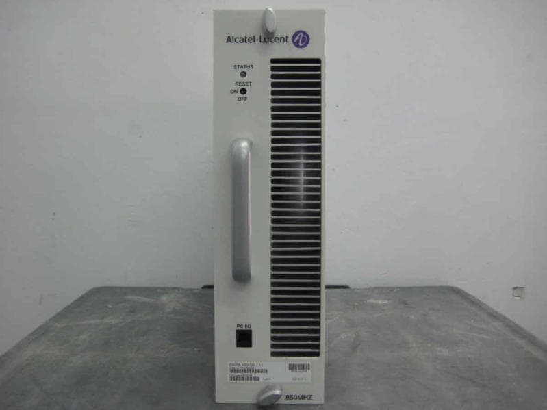
E675JS0123
Nov 03, 2011Multi-carrier RF Power Amplifier
Equipment Class
AMP - Amplifier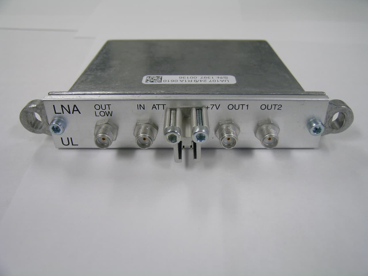
E675JS0120
Aug 26, 2010Nexus Dual Band Repeater
Equipment Class
TNB - Licensed Non-Broadcast Station Transmitter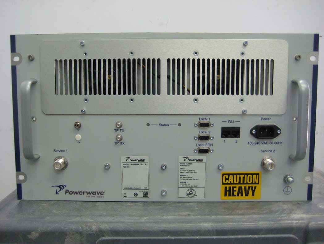
E675JS0119
Aug 01, 2010Nexus Dual Band Repeater
Equipment Class
PCB - PCS Licensed Transmitter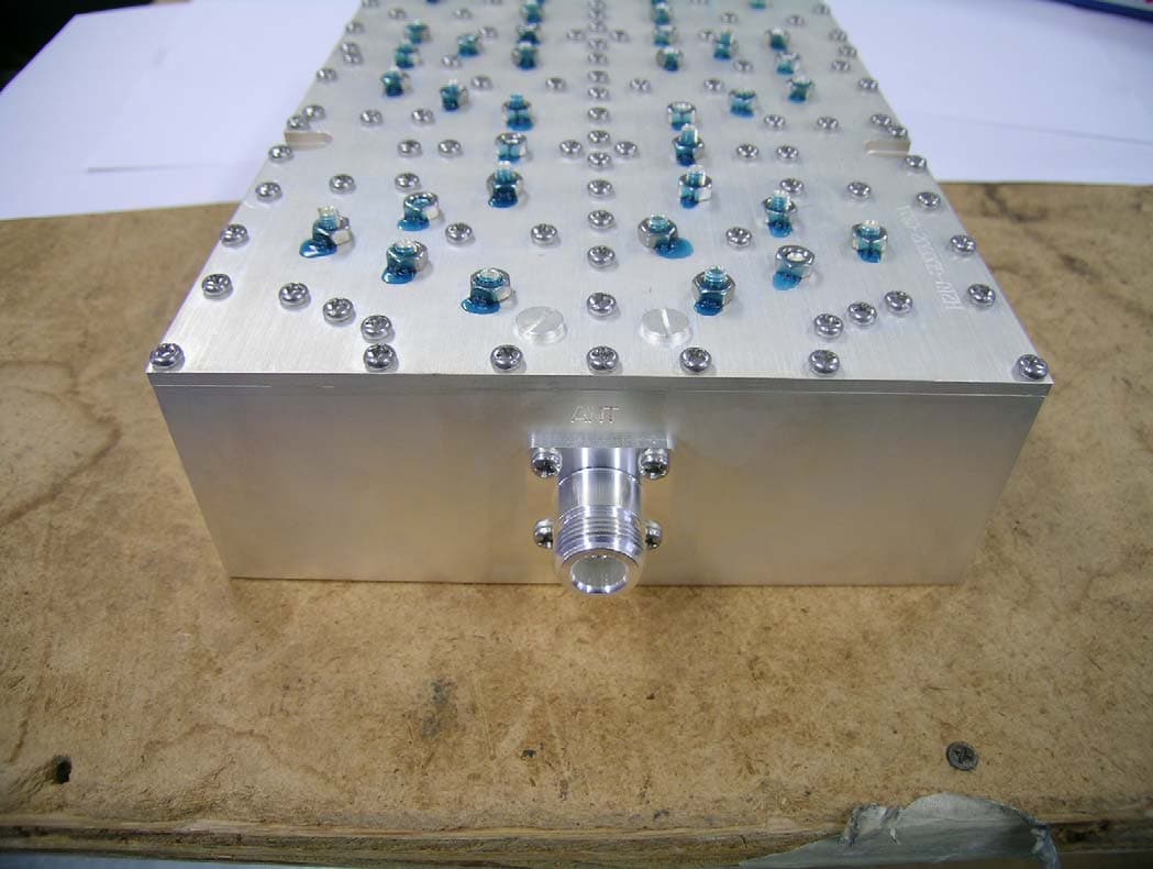
E675JS0118
Jul 26, 2010Nexus Dual Band Repeater
Equipment Class
PCB - PCS Licensed Transmitter
E675JS0096
Jan 10, 2008Wideband Radio Head
Equipment Class
TNB - Licensed Non-Broadcast Station Transmitter