E675JS0071Multi Carrier RF Power Amplifier
Powerwave Technologies Inc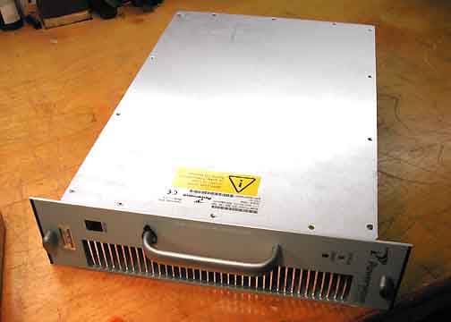
Click to zoom
Application Details
- Equipment Class
- AMP - Amplifier
- Date of Grant
- Jan 06, 2005
- Application Purpose
- Original Equipment
- Date of Application
- Jan 06, 2005
- Equipment Note
- Multi Carrier RF Power Amplifier
- Frequency Range
- 869.00000000 - 894.00000000
- Company
- Powerwave Technologies Inc
- Country
- United States
Documents & Files
Document Text
Text extracted from the exhibit documents filed with the FCC. Open a document above to read the original.
Users Manual
G3L-850-135 Multi-Carrier Power Am plifier Service and Installation Manual 044-05117 December 2004 044-05117 © 2004 Powerwave Technologies Incorporated. All rights reserved. Powerwave Technologies, and the Powerwave logo are registered trademarks Powerwave Technologies, Inc. reserves the right to make changes to the documentation and equipment, including but not limited to component substitution and circuitry changes. Changes that impact this manual may subsequently be incorporated in a later revision of this manual. This Powerwave product is designed to operate within the Normal Operating (typical operating) ranges or conditions specified in this document. Operation of this equipment beyond the specified ranges in this document may cause (1) spurious emissions that violate regulatory requirements; (2) the equipment to be automatically removed from service when maximum thresholds are exceeded; or (3) the equipment to not perform in accordance with its specifications. It is the Operator's responsibility to ensure this equipment is properly installed and operated within Powerwave operating specifications to obtain proper performance from the equipment and to comply with regulatory requirements. ii Installation and Service Manual - G3L-850-135 Multi-Carrier Power Amplifier 044-05117 Warnings, Cautions, and Notes Warnings, cautions, and notes are found throughout this manual. The associated icons in warnings and cautions are used to quickly identify a potential condition that could result in the consequences described below if precautions are not taken. Notes clarify and provide additional information to assist the user. WARNING This warning symbol means danger. You are in a situation that could cause bodily injury. Before you work on any equipment, be aware of the hazards involved with electrical and RF circuitry and be familiar with standard practices for preventing accidents. CAUTIO N This caution symbol means reader, be careful. In this situation, the user might do something that could result in equipment damage or loss of data. Note This note symbol means reader, take note. Notes contain helpful suggestions or references to material not covered in the document. Procedures are not contained in notes. 044-05117 Revision Record Revision Record Revision Letter Date of Entry Reason for Change A December, 2004 Original version of product ii Installation and Service Manual - G3L-850-135 Multi-Carrier Power Amplifier 044-05117 Table of Contents Chapter No. Title Page Chapter 1 General Description 1-1 1-1 Introduction...................................................................................................................1-1 1-2 General Description......................................................................................................1-1 1-3 Functional and Physical Specifications........................................................................1-2 1-4 Ordering Information....................................................................................................1-5 1-5 General Safety..............................................................................................................1-6 1-5.1 Lifting Standards...........................................................................................................1-6 1-5.1.1 Power Plant..................................................................................................................1-6 1-5.1.2 Electronic Modules.......................................................................................................1-6 1-5.1.3 Electrostatic Discharge.................................................................................................1-6 Chapter 2 Installation 2-1 2-1 Introduction...................................................................................................................2-1 2-2 Site Survey...................................................................................................................2-1 2-3 Electrical Service Recommendations...........................................................................2-1 2-4 Air Conditioning............................................................................................................2-2 2-5 Unpacking and Inspection............................................................................................2-3 2-6 Installation Instructions.................................................................................................2-4 2-6.1 Installing the Amplifier into the Subrack.......................................................................2-4 2-6.2 Amplifier Module Power, Alarm, Control, and RF Connector.......................................2-5 Chapter 3 Operating Instructions 3-1 3-1 Introduction...................................................................................................................3-1 3-2 Controls and Indicators................................................................................................3-1 3-2.1 RESET Switch..............................................................................................................3-1 3-2.2 LED Status Indicator and RESET/On/Off Toggle Switch.............................................3-1 3-2.3 RJ-11 PC Interface.......................................................................................................3-2 3-3 Initial Start-Up and Operating Procedures...................................................................3-2 Chapter 4 Principles of Operation 4-1 4-1 Introduction...................................................................................................................4-1 4-2 RF Input Signal.............................................................................................................4-1 4-3 RF Output Load............................................................................................................4-1 4-4 Functional Description............…
Text truncated - open the document above for the full version.
Cover Letter(s)
DC Voltages - 82936 27 Vdc, 3A into the output devices.
External Photos
Overall Top Front Overall Bottom Back
Operational Description
044-05117 Chapter 4 Principles of Operation 4-1 Introduction This chapter contains a functional description of the G3L-850-135 Multi-Carrier Power Amplifier (MCPA). 4-2 RF Input Signal The maximum input power for all carrier frequencies to the amplifier should not exceed the limits specified in Table 1-2 4-3 RF Output Load For good power transfer to the RF load, the load impedance should be as closely matched to the output impedance of the amplifier as possible. A VSWR of less than 1.5:1 across the working band of frequencies is satisfactory. If the amplifier is operated into a filter, it maintains its distortion characteristics outside the signal band even if the VSWR is infinite. A parasitic signal of less than one-watt incident on the output will not cause distortion at a higher level than the normal forward distortion (i.e. -65 dBc). 4-4 Functional Description The Multi-Carrier Power Amplifier (MCPA) is a linear, feedforward amplifier that operates in the frequency band from 869 MHz to 894 MHz with an instantaneous bandwidth of less than 25 MHz (refer to Table 1-2 for amplifier specifications). The instantaneous bandwidth is the maximum frequency band that a set of two or more signals can occupy .The amplifier’s instantaneous bandwidth is set automatically and does not require any manual setup. The amplifier provides a gain of 63 dB. Typical outputs for different carrier types are specified in Table 1-2. Each amplifier is a self-contained module and is functionally independent of any other MCPA in a system. The amplifiers are designed for parallel operation to achieve a high peak power output. Each MCPA has an alarm board that monitors the amplifier performance. If a failure or fault occurs in an MCPA, it is transmitted to a subrack system via the D-sub 21WA4 connector located at the rear of the module. The subrack reports all alarms to the host system. Continuously comparing active paths with passive references, and correcting for small variations through RF feedback controls maintain constant gain. All gain variations, for example those due to temperature, are reduced to the passive reference variations. Refer to Figure 4-1 for the amplifier functional block diagram. The amplifier consists of the following major functional blocks: • Preamplifier • Main amplifier • Error amplifier • Alarm monitoring and control • First and second loop control circuits • Pilot tone generator Installation and Service Manual - G3L-850-135 Multi-Carrier Power Amplifier 4-1 044-05117 Figure 4-1. Functional Block Diagram 4-4.1 Preamplifier The RF carriers are applied to the input port of the amplifier, where they are fed to the preamplifier stage. The preamplifier provides two stages of class-A mode-amplification. The output of the preamplifier is then split into two paths, one to the main amplifier and one to the error amplifier. 4-4.2 Main and Error Amplifiers The main amplifier provides the balance of gain and power (refer to Table 1-1 for amplifier specifications). The main amplifier employs class AB amplification for maximum efficiency. The error amplifier and feed forward loops are used to correct signal distortion introduced by non- linearity in the class AB main amplifier. The error amplifier operates in class A mode. The RF signal from the preamp is coupled to an attenuator and phase shifter in the first feed-forward loop where it is phase shifted by 180 degrees and amplified in the pre-main amplifier. The output from the pre-main amplifier is fed to the class AB main amplifier. The signal output from the main amplifier is sampled using a coupler, and the sample signal is combined with the main input signal and input to the second feed-forward loop. The error signal is attenuated, phase shifted 180 degrees, then fed to the error amplifier where it is amplified to a level identical to the sample output from the main amplifier. The output from the error amplifier is then coupled back and added to the output from the main amplifier. The control loops continuously make adjustments to cancel out any distortion in the final output signals. 4-4.3 Alarm Monitoring and Control The alarm logic controls the +5 Vdc bias voltage that shuts down the amplifier. During routine operation, all normal variations are automatically compensated for by the feed-forward loop control. However, when large variations occur beyond the adjustment range of the loop control, a 4-2 Installation and Service Manual - G3L-850-135 Multi-Carrier Power Amplifier 044-05117 loop fault occurs. When this happens, an alarm indicator is illuminated on the front panel of the subrack. The fault is transmitted back to an external summary module via the external alarm interface connection on the front panel of the subrack. 4-4.4 First and Second Loop Control Circuits The primary function of the first loop is to amplify the carrier signals and isolate an error signal for the second loop. The primary function of the second loop is to amplify the error signal to cancel out spurious products developed in the main amplifier. The input signal is amplified by a preamplifier and fed to a coupler and delay line. The signal from the coupler is fed to the attenuator and phase shifter in the first loop. The first loop control section phase shifts the main input signals by 180 degrees and constantly monitors the output for correct phase and gain. The second loop control section obtains a sample of the distortion added to the output signals by the main amplifiers. The signal is phase shifted 180 degrees, then fed to the error amplifier where it is amplified to the same power level as the input sample. The signal is then coupled to the error signal of the main amplifier output. The final output is monitored by the second loop and adjusted to ensure that the signal distortion and intermodulation distortion (IMD) on the final output is cancelled out. 4-4.5 Pilot Tone Generator A Pilot Tone is an internally generated signal, who’s precise frequency, phase, and …
Text truncated - open the document above for the full version.
Test Report
Page 1 of 63 Report No.: FC04-086 POWERWAVE TECHNOLOGIES TEST REPORT FOR THE POWER AMPLIFIER, G3L-850-135 FCC PART 22 AND RSS-131 COMPLIANCE DATE OF ISSUE: DECEMBER 7, 2004 PREPARED FOR: Powerwave Technologies 1801 E. St. Andrew Place Santa Ana, CA 92705 PREPARED BY: Mary Ellen Clayton CKC Laboratories, Inc. 5473A Clouds Rest Mariposa, CA 95338 W.O. No.: 82936Date of test: November 16-30, 2004 Report No.: FC04-086 This report contains a total of 63 pages and may be reproduced in full only. Partial reproduction may only be done with the written consent of CKC Laboratories, Inc. The results in this report apply only to the items tested, as identified herein. Page 2 of 63 Report No.: FC04-086 TABLE OF CONTENTS Administrative Information .............................................................................................3 Summary of Results .........................................................................................................4 Conditions for Compliance ..............................................................................................4 Approvals .........................................................................................................................4 Equipment Under Test (EUT) Description ......................................................................5 Equipment Under Test .....................................................................................................5 Peripheral Devices ...........................................................................................................5 Temperature and Humidity During Testing.....................................................................6 FCC 2.1033(c)(3) User’s Manual ....................................................................................6 FCC 2.1033(c)(4) Type of Emissions ..............................................................................6 FCC 2.1033(c)(5) Frequency Range................................................................................6 FCC 2.1033(c)(6) Operating Power.................................................................................6 FCC 2.1033(c)(7) Maximum Power Rating ....................................................................6 FCC 2.1033(c)(8) DC Voltages .......................................................................................6 FCC 2.1033(c)(9) Tune-Up Procedure ............................................................................6 FCC 2.1033(c)(10) Schematics and Circuitry Description..............................................6 FCC 2.1033(c)(11) Label and Placement ........................................................................6 FCC 2.1033(c)(12) Submittal Photos ..............................................................................6 FCC 2.1033(c)(13) Modulation Information ...................................................................6 FCC 2.1033(c)(14)/2.1046/22.913 - RF Power Output ...................................................7 FCC 2.1033(c)(14)/2.1047(b) - Audio Frequency Response...........................................8 FCC 2.1033(c)(14)/2.1047(b) - Modulation Limiting Response.....................................8 FCC 2.1033(c)(14)/2.1051/22.917(a) - Spurious Emissions at Antenna Terminal .........9 FCC 2.1033(c)(14)/2.1053/22.917(a) - Field Strength of Spurious Radiation ................15 Input Plots GSM ..............................................................................................................21 Output Plots GSM............................................................................................................24 Input Plots EDGE ............................................................................................................27 Output Plots EDGE..........................................................................................................30 Input Plots WCDMA .......................................................................................................33 Output Plots WCDMA.....................................................................................................36 Blockedge Plots GSM......................................................................................................40 Blockedge Plots EDGE....................................................................................................42 Blockedge Plots WCDMA...............................................................................................44 Intermodulation................................................................................................................47 99% Bandwidth Plots GSM .............................................................................................51 99% Bandwidth Plots EDGE ...........................................................................................54 99% Bandwidth Plots WCDMA ......................................................................................57 RSS-131 Section 6.2 ........................................................................................................61 Page 3 of 63 Report No.: FC04-086 ADMINISTRATIVE INFORMATION DATE OF TEST: November 16-30, 2004 DATE OF RECEIPT: November 16, 2004 PURPOSE OF TEST: To demonstrate the compliance of the Power Amplifier, G3L-850-135 with the requirements for FCC Part 22 and RSS-131devices. TEST METHOD: FCC Part 22 and RSS-212 FREQUENCY RANGE TESTED: 9 kHz-9 GHz MANUFACTURER: Powerwave Technologies 1801 E. St. Andrew Place Santa Ana, CA 92705 REPRESENTATIVE: Jeffrey Dale TEST LOCATION: CKC Laboratories, Inc. 110 Olinda Place Brea, CA 92621 Page 4 of 63 Report No.: FC04-086 SUMMARY OF RESULTS As received, the Powerwave Technologies Power Amplifier, G3L-850-135 was found to be fully compliant with the following standards and specifications: Canadian Standard Canadian Section FCC Standard FCC Section Test Description RSS-1315.4NANAExternal Controls RSS-1315.547 CFR1.…
Text truncated - open the document above for the full version.
Test Setup Photos
RF POWER OUTPUT PHOTOGRAPH SHOWING DIRECT CONNECT TEST SETUP PHOTOGRAPH SHOWING RADIATED EMISSIONS Radiated Emissions - Front View PHOTOGRAPH SHOWING RADIATED EMISSIONS Radiated Emissions - Back View INPUT VS OUTPUT BLOCKEDGE INTERMODULATION 99% BANDWIDTH RSS-131 SECTION 6.2
Contact Information
Applicant
Jeff Dale(Principal Reliability Engineer)
Technical Contact
CKC Laboratories, Inc.Mary Ellen Clayton
[email protected]209-966-5240
5473-A Clouds Rest · Mariposa, California · United States
Test Firm
CKC Laboratories, Inc.Steve Behm
Technical Specifications
| # | Rule Parts | Frequency Range | Power Output | Emission | Tolerance |
|---|---|---|---|---|---|
| 3 | 22H | 869 MHz - 894 MHz | 145 W | GXW | Amp |
Other Applications from Powerwave Technologies Inc
E675JS0123
Nov 03, 2011Multi-carrier RF Power Amplifier
Equipment Class
AMP - Amplifier
E675JS0120
Aug 26, 2010Nexus Dual Band Repeater
Equipment Class
TNB - Licensed Non-Broadcast Station Transmitter
E675JS0119
Aug 01, 2010Nexus Dual Band Repeater
Equipment Class
PCB - PCS Licensed Transmitter
E675JS0118
Jul 26, 2010Nexus Dual Band Repeater
Equipment Class
PCB - PCS Licensed Transmitter
E675JS0096
Jan 10, 2008Wideband Radio Head
Equipment Class
TNB - Licensed Non-Broadcast Station Transmitter