EZZ6138Channelized Signal Booster
Bird Technologies Group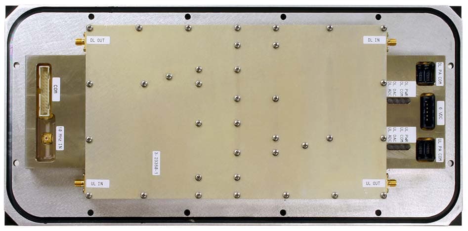
Click to zoom
Application Details
- Equipment Class
- TNB - Licensed Non-Broadcast Station Transmitter
- Date of Grant
- Sep 21, 2011
- Application Purpose
- Original Equipment
- Date of Application
- Sep 20, 2011
- Equipment Note
- Channelized Signal Booster
- Frequency Range
- 806.00000000 - 824.00000000
- Company
- Bird Technologies Group
- Country
- United States
Documents & Files
Document Text
Text extracted from the exhibit documents filed with the FCC. Open a document above to read the original.
Users Manual
YOU'RE HEARD, LOUD AND CLEAR. 8625 Industrial Parkway, Angola, NY 14006 Tel: 716-549-4700 Fax: 716-549-4772 [email protected] www.bird-technologies.com Installation and Operation Manual for the SBIII Digital Signal Booster Model 613-8 Manual Part Number 7-9485 DIGITAL TECHNOLOGY Warranty This warranty applies for one year from shipping date. TX RX Systems Inc. warrants its products to be free from defect in material and workmanship at the time of shipment. Our obligation under warranty is limited to replacement or repair, at our option, of any such products that shall have been defective at the time of manufacture. TX RX Systems Inc. reserves the right to replace with merchandise of equal performance although not identical in every way to that originally sold. TX RX Systems Inc. is not liable for dam- age caused by lightning or other natural disasters. No product will be accepted for repair or replacement without our prior written approval. The purchaser must prepay all shipping charges on returned products. TX RX Systems Inc. shall in no event be liable for consequential damages, installation costs or expense of any nature resulting from the purchase or use of products, whether or not they are used in accordance with instructions. This warranty is in lieu of all other warranties, either expressed or implied, including any implied warranty or merchantability of fitness. No repre- sentative is authorized to assume for TX RX Systems Inc. any other liability or warranty than set forth above in con- nection with our products or services. TERMS AND CONDITIONS OF SALE PRICES AND TERMS: Prices are FOB seller’s plant in Angola, NY domestic packaging only, and are subject to change without notice. Fed- eral, State and local sales or excise taxes are not included in prices. When Net 30 terms are applicable, payment is due within 30 days of invoice date. All orders are subject to a $100.00 net minimum. QUOTATIONS: Only written quotations are valid. ACCEPTANCE OF ORDERS: Acceptance of orders is valid only when so acknowledged in writing by the seller. SHIPPING: Unless otherwise agreed at the time the order is placed, seller reserves the right to make partial shipments for which payment shall be made in accordance with seller’s stated terms. Shipments are made with transportation charges col- lect unless otherwise specified by the buyer. Seller’s best judgement will be used in routing, except that buyer’s routing is used where practicable. The seller is not responsible for selection of most economical or timeliest routing. CLAIMS: All claims for damage or loss in transit must be made promptly by the buyer against the carrier. All claims for shortages must be made within 30 days after date of shipment of material from the seller’s plant. SPECIFICATION CHANGES OR MODIFICATIONS: All designs and specifications of seller’s products are subject to change without notice provided the changes or modifi- cations do not affect performance. RETURN MATERIAL: Product or material may be returned for credit only after written authorization from the seller, as to which seller shall have sole discretion. In the event of such authorization, credit given shall not exceed 80 percent of the original pur- chase. In no case will Seller authorize return of material more than 90 days after shipment from Seller’s plant. Credit for returned material is issued by the Seller only to the original purchaser. ORDER CANCELLATION OR ALTERATION: Cancellation or alteration of acknowledged orders by the buyer will be accepted only on terms that protect the seller against loss. NON WARRANTY REPAIRS AND RETURN WORK: Consult seller’s plant for pricing. Buyer must prepay all transportation charges to seller’s plant. Standard shipping pol- icy set forth above shall apply with respect to return shipment from TX RX Systems Inc. to buyer. DISCLAIMER Product part numbering in photographs and drawings is accurate at time of printing. Part number labels on TX RX products supersede part numbers given within this manual. Information is subject to change without notice. Bird Technologies Group TX RX Systems Inc. Symbols Commonly Used WARNING ESD Electrostatic Discharge Hot Surface Electrical Shock Hazard Important Information CAUTION or ATTENTION High Voltage Heavy Lifting Bird Technologies GroupTX RX Systems Inc. NOTE Manual Part Number 7-9485 Copyright © 2011 TX RX Systems, Inc. First Printing: May 2011 Version NumberVersion Date 105/16/11 1.407/25/11 1.609/02/11 1.709/12/11 Contact Information Changes to this Manual Bird Technologies GroupTX RX Systems Inc. Sales Support at 716-217-3113 Customer Service at 716-217-3144 Technical Publications at 716-549-4700 extension 5019 We have made every effort to ensure this manual is accurate. If you discover any errors, or if you have suggestions for improving this manual, please send your comments to our Angola, New York facility to the attention of the Technical Publications Department. This manual may be periodically updated. When inquiring about updates to this manual refer to the manual part number and revision number on the revision page following the front cover. Table of Contents Manual 7-9485-1.7 09/12/11 Table of Contents Overview............................................................................................................... 1 Down / Up Conversion......................................................................................... 2 Unpacking ............................................................................................................ 3 Installation............................................................................................................ 3 Location ............................................................................................................. 3 Mounting............................................................................................................. 3 Connections...............................................................…
Text truncated - open the document above for the full version.
External Photos
Channelized Signal Booster (Model 613-8) - External Photos (revision 1) Channel Module 3-23350-1, 3-23368-1, 3-23919, 3-23920, 3-23921, 3-23922, 3-23923, 3-23924 top left side view (3-23350 shown as example, all modules have same physical appearance except for the part number sticker). Channel Module 3-23350-1, 3-23368-1, 3-23919, 3-23920, 3-23921, 3-23922, 3-23923, 3-23924 top right side view (3-23350 shown as example, all modules have same physical appearance except for the part number sticker). Channelized Signal Booster (Model 613-8) - External Photos (revision 1) Channel Module 3-23350-1, 3-23368-1, 3-23919, 3-23920, 3-23921, 3-23922, 3-23923, 3-23924 top view (3-23350 shown as example, all modules have same physical appearance except for the part number sticker).
External Photos
Channelized Signal Booster (Model 613-8) - External Photos Control Board 3-23360 front-right view. Control Board 3-23360 rear-right view. Channelized Signal Booster (Model 613-8) - External Photos Control Board 3-23360 top view. Control Board 3-23350 side view. Channelized Signal Booster (Model 613-8) - External Power Amplifier 3-23365 top front view. Power Amplifier 3-23365 top rear view. Channelized Signal Booster (Model 613-8) - External Photos Power Amplifier 3-23365 top view. Power Amplifier 3-23365 front view. Power Amplifier 3-23365 rear view. Channelized Signal Booster (Model 613-8) - External Photos AC Power Supply 3-23912 left side view. AC Power Supply 3-23912 right side view. Channelized Signal Booster (Model 613-8) - External Photos AC Power Supply 3-23912 AC Input close-up. AC Power Supply 3-23912 DC Output close-up. Channelized Signal Booster (Model 613-8) - External Photos DC - DC Converter 3-23913 top left view. DC - DC Converter 3-23913 top right view. Channelized Signal Booster (Model 613-8) - External Photos DC - DC Converter 3-23913 top view. DC - DC Converter 3-23913 side view. Channelized Signal Booster (Model 613-8) - External Photos Directional Coupler 3-5688 top view. Directional Coupler 3-5688 bottom view. Channelized Signal Booster (Model 613-8) - External Photos Directional Coupler 3-5688 front-right view. Directional Coupler 3-5688 front-left view. Channelized Signal Booster (Model 613-8) - External Photos Triplexer 8-23088 top left view. Triplexer 8-23088 top right view. Channelized Signal Booster (Model 613-8) - External Photos Triplexer 8-23088 left side view. Triplexer 8-23088 right side view. Triplexer 8-23088 top view. Channelized Signal Booster (Model 613-8) - External Photos Line Filter 8-23887 left side view. Line Filter 8-23887 right side view. Line Filter 8-23887 top view. Channelized Signal Booster (Model 613-8) - External Photos Line Filter 8-23909 top left view. Line Filter 8-23909 top right view. Channelized Signal Booster (Model 613-8) - External Photos Line Filter 8-23909 right side view. Line Filter 8-23909 top view. Channelized Signal Booster (Model 613-8) - External Photos Channel Module top left side view (3-23350 shown as an example). Channel Module top right side view (3-23350 shown as an example). Channelized Signal Booster (Model 613-8) - External Photos Channel Module top view (3-23350 shown as an example). Channelized Signal Booster (Model 613-8) - External Photos Enclosure front view. Channelized Signal Booster (Model 613-8) - External Photos Enclosure top view. Enclosure bottom view. Channelized Signal Booster (Model 613-8) - External Photos Enclosure left view. Enclosure right view.
ID Label/Location Info
This device complies with part 15 of the FCC rules. Operation is subject to the following two conditions: (1) This device may not cause harmful interference and (2) this device must accept any interference received, including interference that may cause undesired operation. Bird Technologies TX RX Systems, Inc. Model: 613-8 FCC ID: EZZ6138 IC: 1940A-6138 Bird Technologies TX RX Systems, Inc. Serial Number: PRE-PRODUCTION 001
Internal Photos
Channelized Signal Booster (Model 613-8) - Internal Photos Channel Module Oscillator board 3-23351-1 top view. Channel Module Oscillator board 3-23351-1 bottom view. Channelized Signal Booster (Model 613-8) - Internal Photos Channel Module Oscillator board 3-23351-2 top view. Channel Module Oscillator board 3-23351-2 bottom view. Channelized Signal Booster (Model 613-8) - Internal Photos Channel Module Oscillator board 3-23351-3 top view. Channel Module Oscillator board 3-23351-3 bottom view. Channelized Signal Booster (Model 613-8) - Internal Photos Channel Module Oscillator board 3-23351-4 top view. Channel Module Oscillator board 3-23351-4 bottom view. Channelized Signal Booster (Model 613-8) - Internal Photos Channel Module Digital board 3-23353-1 top view. Channelized Signal Booster (Model 613-8) - Internal Photos Channel Module Digital board 3-23353-1 top view. Channelized Signal Booster (Model 613-8) - Internal Photos Channel Module Digital board 3-23353-2 top view. Channelized Signal Booster (Model 613-8) - Internal Photos Channel Module Digital board 3-23353-2 bottom view. Channelized Signal Booster (Model 613-8) - Internal Photos Channel Module Downconverter board 3-23355-1 top view. Channel Moule Downconverter board 3-23355-1 bottom view. Channelized Signal Booster (Model 613-8) - Internal Photos Channel Module Downconverter board 3-23355-2 top view. Channel Module Downconverter board 3-23355-2 bottom view. Channelized Signal Booster (Model 613-8) - Internal Photos Channel Module Downconverter board 3-23355-3 top view. Channel Module Downconverter board 3-23355-3 bottom view. Channelized Signal Booster (Model 613-8) - Internal Photos Channel Module Downconverter board 3-23355-4 top view. Channel Module Downconverter board 3-23355-4 bottom view. Channelized Signal Booster (Model 613-8) - Internal Photos Channel Module Upconverter board 3-23357-1 top view. Channel Module Upconverter board 3-23357-1 bottom view. Channelized Signal Booster (Model 613-8) - Internal Photos Channel Module Upconverter board 3-23357-2 top view. Channel Module Upconverter board 3-23357-2 bottom view. Channelized Signal Booster (Model 613-8) - Internal Photos Channel Module Upconverter board 3-23357-3 top view. Channel Module Upconverter board 3-23357-3 bottom view. Channelized Signal Booster (Model 613-8) - Internal Photos Channel Module Upconverter board 3-23357-4 top view. Channel Module Upconverter board 3-23357-4 bottom view. Channelized Signal Booster (Model 613-8) - Internal Photos Channel Module Upconverter board 3-23357-5 top view. Channel Module Upconverter board 3-23357-5 bottom view. Channelized Signal Booster (Model 613-8) - Internal Photos Channel Module Upconverter board 3-23357-6 top view. Channel Module Upconverter board 3-23357-6 bottom view. Channelized Signal Booster (Model 613-8) - Internal Photos Channel Module Upconverter board 3-23357-7 top view. Channel Module upconverter board 3-23357-7 bottom view. Channelized Signal Booster (Model 613-8) - Internal Photos Channel Module Upconverter board 3-23357-8 top view. Channel Module Upconverter board 3-23357-8 bottom view. Channelized Signal Booster (Model 613-8) - Internal Photos Control Board 3-23361 front view. (used in subassembly 3-23360) Control Board 3-23361 back view. (used in subassembly 3-23360) Channelized Signal Booster (Model 613-8) - Internal Photos Power Amplifier Board 3-23366 front view. (used in subassembly 3-23912) Power Amplifier Board 3-23366 back view. (used in subassembly 3-23912) Channelized Signal Booster (Model 613-8) - Internal Photos Directional Coupler 3-5688 internal view bottom. Directional Coupler 3-5688 Internal view bottom left. Channelized Signal Booster (Model 613-8) - Internal Photos Directional coupler board 4-5435 front view. (used in subassembly 3-5688) Directional coupler board 4-5435 rear view. (used in subassembly 3-5688)
Operational Description
Dual 8-/10-/12-/14-/16-Bit 250 MSPS Digital-to-Analog Converters AD9741/AD9743/AD9745/AD9746/AD9747 Rev. 0 Information furnished by Analog Devices is believed to be accurate and reliable. However, no responsibility is assumed by Analog Devices for its use, nor for any infringements of patents or other rights of third parties that may result from its use. Specifications subject to change without notice. No license is granted by implication or otherwise under any patent or patent rights of Analog Devices. Trademarks and registered trademarks are the property of their respective owners. One Technology Way, P.O. Box 9106, Norwood, MA 02062-9106, U.S.A. Tel: 781.329.4700 www.analog.com Fax: 781.461.3113 ©2007 Analog Devices, Inc. All rights reserved. FEATURES High dynamic range, dual DACs Low noise and intermodulation distortion Single carrier WCDMA ACLR = 80 dBc @ 61.44 MHz IF Innovative switching output stage permits useable outputs beyond Nyquist frequency LVCMOS inputs with dual-port or optional interleaved single-port operation Differential analog current outputs are programmable from 8.6 mA to 31.7 mA full scale Auxiliary 10-bit current DACs with source/sink capability for external offset nulling Internal 1.2 V precision reference voltage source Operates from 1.8 V and 3.3 V supplies 315 mW power dissipation Small footprint, Pb-free, 72-Lead LFCSP APPLICATIONS Wireless infrastructure: WCDMA, CDMA2000, TD-SCDMA, WiMAX Wideband communications: LMDS/MMDS, point-to-point Instrumentation: RF signal generators, arbitrary waveform generators GENERAL DESCRIPTION The AD9741/AD9743/AD9745/AD9746/AD9747 are pin- compatible, high dynamic range, dual digital-to-analog converters (DACs) with 8-/10-/12-/ 14-/16-bit resolutions and sample rates of up to 250 MSPS. The devices include specific features for direct conversion transmit applications, including gain and offset compensation, and they interface seamlessly with analog quadrature modulators, such as the ADL5370. A proprietary, dynamic output architecture permits synthesis of analog outputs even above Nyquist by shifting energy away from the fundamental and into the image frequency. Full programmability is provided through a serial peripheral interface (SPI) port. In addition, some pin-programmable features are offered for those applications without a controller. PRODUCT HIGHLIGHTS 1. Low noise and intermodulation distortion (IMD) enables high quality synthesis of wideband signals. 2. Proprietary switching output for enhanced dynamic performance. 3. Programmable current outputs and dual auxiliary DACs provide flexibility and system enhancements. FUNCTIONAL BLOCK DIAGRAM 16-BIT DAC1 16-BIT DAC2 INTERFACE LOGIC GAIN DAC GAIN DAC OFFSET DAC OFFSET DAC INTERNAL REFERENCE AND BIAS REFIO FSADJ SERIAL PERIPHERAL INTERFACE SDO SDIO SCLK CSB 10 CMOS INTERFACE CLKP CLKN PID<15:0> P2D<15:0> IOUT1P IOUT1N IOUT2P IOUT2N AUX1P AUX1N AUX2P AUX2N 06569-001 Figure 1. AD9741/AD9743/AD9745/AD9746/AD9747 Rev. 0 | Page 2 of 28 TABLE OF CONTENTS Features .............................................................................................. 1 Applications....................................................................................... 1 General Description ......................................................................... 1 Product Highlights ........................................................................... 1 Functional Block Diagram .............................................................. 1 Revision History ............................................................................... 2 Specifications..................................................................................... 3 DC Specifications ......................................................................... 3 AC Specifications.......................................................................... 5 Digital and Timing Specifications.............................................. 7 Absolute Maximum Ratings............................................................ 8 Thermal Resistance ...................................................................... 8 ESD Caution.................................................................................. 8 Pin Configurations and Function Descriptions ........................... 9 Typical Performance Characteristics ........................................... 14 Terminology .................................................................................... 17 Theory of Operation ...................................................................... 18 Serial Peripheral Interface ......................................................... 18 General Operation of the Serial Interface ............................... 18 Instruction Byte .......................................................................... 18 MSB/LSB Transfers .................................................................... 19 Serial Interface Port Pin Descriptions ..................................... 19 SPI Register Map ............................................................................ 20 SPI Register Descriptions .............................................................. 21 Digital Inputs and Outputs ........................................................... 22 Input Data Timing ..................................................................... 22 Dual-Port Mode Timing ........................................................... 22 Single-Port Mode Timing ......................................................... 22 SPI Port, Reset, and Pin Mode.................................................. 22 Driving the DAC Clock Input .................................................. 23 Full-Scale Current Generation ................................................. 23 DAC Transfer Function ............................................................. 24 Analog Modes of Operation ..................................................... 24 Aux…
Text truncated - open the document above for the full version.
Operational Description
LTC6400-20 8 640020f FREQUENCY (MHz) THIRD ORDER IMD (dBc) –40 –50 –60 –80 –90 –70 –100 640020 G17 050100150200250300 UNFILTERED NO R L UNFILTERED 200Ω R L FILTERED NO R L SINGLE-ENDED INPUT V OUT = 2V P-P COMPOSITE FREQUENCY (MHz) THIRD ORDER IMD (dBc) –40 –50 –60 –80 –90 –70 –110 –100 640020 G14 UNFILTERED NO R L UNFILTERED 200Ω R L FILTERED NO R L DIFFERENTIAL INPUT V OUT = 2V P-P COMPOSITE 050100150200250300 FREQUENCY (MHz) HARMONIC DISTORTION (dBc) –40 –50 –60 –80 –90 –70 –100 640020 G15 HD2 NO R L HD2 200Ω R L HD3 NO R L HD3 200Ω R L SINGLE-ENDED INPUT V OUT = 2V P-P 050100150200250300 FREQUENCY (MHz) HARMONIC DISTORTION (dBc) –40 –50 –60 –80 –90 –70 –100 640020 G16 HD2 HD3 SINGLE-ENDED INPUT V OUT = 2V P-P NO R L 050100150200250300 TIME (ns) 0 OUTPUT VOLTAGE (V) 2.5 0.5 1.0 2.0 1.5 0 50100150 200 640020 G10 –OUT R L = 87.5Ω PER OUTPUT +OUT TIME (ns) 0 SETTLING (%) 5 4 3 2 1 –4 –3 –2 –1 –5 0 0.51.01.52.52.0 3.0 640020 G11 R L = 87.5Ω PER OUTPUT TYPICAL PERFORMANCE CHARACTERISTICS Overdrive Recovery Time 1% Settling Time for 2V Output Step Harmonic Distortion (Unfi ltered) vs Frequency Harmonic Distortion (Filtered) vs Frequency Third Order Intermodulation Distortion vs Frequency Harmonic Distortion (Unfi ltered) vs Frequency Harmonic Distortion (Filtered) vs Frequency Harmonic Distortion vs Output Common Mode Voltage (Unfi ltered Outputs) FREQUENCY (MHz) 050 HARMONIC DISTORTION (dBc) –40 –50 –60 –80 –90 –70 –100 100150200250300 640020 G12 HD2 NO R L HD2 200Ω R L HD3 NO R L HD3 200Ω R L DIFFERENTIAL INPUT V OUT = 2V P-P FREQUENCY (MHz) HARMONIC DISTORTION (dBc) –40 –50 –60 –80 –90 –70 –100 640020 G13 HD2 HD3 DIFFERENTIAL INPUT V OUT = 2V P-P NO R L 050100150200250300 Third Order Intermodulation Distortion vs Frequency OUTPUT COMMON MODE VOLTAGE (V) 1.01.11.21.31.4 1.5 640020 G18 HD2 HD3 HARMONIC DISTORTION (dBc) –40 –50 –60 –80 –90 –70 –100 V OUT = 2V P-P at 100MHz R L = 400Ω LTC6400-20 9 640020f TIME (ns) 0–100 VOLTAGE (V) 3.5 2.0 2.5 1.0 1.5 3.0 –0.5 0.5 0 SUPPLY CURRENT (mA) 140 80 100 40 60 120 –20 20 0 100200300400 500 640020 G21 +OUT –OUT I CC ENABLE R L = 87.5Ω PER OUTPUT VOLTAGE (V) 3.5 2.0 2.5 1.0 1.5 3.0 –0.5 0.5 0 SUPPLY CURRENT (mA) 140 80 100 40 60 120 –20 20 0 640020 G22 +OUT –OUT ENABLE I CC R L = 87.5Ω PER OUTPUT TIME (ns) 0–100100200300400500 FREQUENCY (MHz) 50 OUTPUT 1dB COMPRESSION (dBm) 20 19 18 16 17 15 100150200250300 640020 G19 DIFFERENTIAL INPUT R L = 400Ω (NOTE 7) FREQUENCY (MHz) OUTPUT IP3 (dBm) 60 50 40 20 10 30 0 640020 G20 UNFILTERED NO R L UNFILTERED 200Ω R L FILTERED NO R L DIFFERENTIAL INPUT V OUT = 2V P-P COMPOSITE (NOTE 7) 050100150200250300 TYPICAL PERFORMANCE CHARACTERISTICS Output 1dB Compression Point vs Frequency Output Third Order Intercept vs Frequency Turn-On TimeTurn-Off Time LTC6400-20 10 640020f BLOCK DIAGRAM PIN FUNCTIONS V + (Pins 1, 3, 10): Positive Power Supply (Normally tied to 3V or 3.3V). All three pins must be tied to the same voltage. Bypass each pin with 1000pF and 0.1μF capaci- tors as close to the pins as possible. V OCM (Pin 2): This pin sets the output common mode voltage. A 0.1μF external bypass capacitor is recom- mended. V – (Pins 4, 9, 12, 17): Negative Power Supply (GND). All four pins must be connected to same voltage/ground. –OUT, +OUT (Pins 5, 8): Unfi ltered Outputs. These pins have series resistors, R OUT 12.5Ω. –OUTF, +OUTF (Pins 6, 7): Filtered Outputs. These pins have 50Ω series resistors and a 2.7pF shunt capacitor. ⎯ E ⎯ N ⎯ A ⎯ B ⎯ L ⎯ E (Pin 11): This pin is a logic input referenced to V EE . If low, the part is enabled. If high, the part is disabled and draws approximately 1mA supply current. +IN (Pins 13, 14): Positive Input. Pins 13 and 14 are internally shorted together. –IN (Pins 15, 16): Negative Input. Pins 15 and 16 are internally shorted together. Exposed Pad (Pin 17): V – . The Exposed Pad must be connected to same voltage/ground as pins 4, 9, 12. 13 640020 BD 1 V + 2 V OCM 14 7 15 +OUT +OUTF –OUTF –OUT +IN IN+OUT– IN–OUT+ +IN –IN –IN 516 R G 100Ω R OUT 12.5Ω R F 1000Ω R G 100Ω 2k R F 1000Ω 6 4 V – 3 V + 12 V – 11 ENABLE 9 V – 10 V + COMMON MODE CONTROL BIAS CONTROL 8 R OUT 12.5Ω R FILT 50Ω R FILT 50Ω C FILT 1.7pF 5.3pF LTC6400-20 11 640020f APPLICATIONS INFORMATION Circuit Operation The LTC6400 is a low noise and low distortion fully dif- ferential op amp/ADC driver with: • Operation from DC to 1.8GHz (–3dB bandwidth) • Fixed gain of 10V/V (20dB) • Differential input impedance 200Ω • Differential output impedance 25Ω • On-Chip 590MHz output fi lter The LTC6400 is composed of a fully differential amplifi er with on chip feedback and output common mode voltage control circuitry. Differential gain and input impedance are set by 100Ω/1000Ω resistors in the feedback network. Small output resistors of 12.5Ω improve the circuit stability over various load conditions. They also provide a possible external fi ltering option, which is often desirable when the load is an ADC. Filter resistors of 50Ω are available for additional fi ltering. Lowpass/bandpass fi lters are easily implemented with just a couple of external components. Moreover, they offer single-ended 50Ω matching in wideband applications and no external resistor is needed. The LTC6400-20 is very fl exible in terms of I/O coupling. It can be AC- or DC-coupled at the inputs, the outputs or both. Due to the internal connection between input and output, users are advised to keep input common mode voltage between 1V and 1.6V for proper operation. If the inputs are AC-coupled, the input common mode voltage is automatically biased close to V OCM and thus no external circuitry is needed for bias. The LTC6400-20 provides an output common mode voltage set by V OCM , which allows driving an ADC directly without external components such as a transformer or AC coupling capacitors. The input signal can be either single-ended or differential with only minor differences in distortion performance. Input Impedance and Matching The differential input impedance of …
Text truncated - open the document above for the full version.
Operational Description
Channelized Signal Booster (Model 613-8) - Operational Description (revision 3) OPERATIONAL DESCRIPTION The signal booster system transmits into a distrib- uted antenna system (DAS) for downlink output signals and a DONOR antenna for uplink output signals. The DAS usually has a gain of 0 dBi or less, with only 2 antenna elements a splitter and cable loss the gain adds up to roughly -4 dBi (-6.15 dBd). If higher gain antenna are used (higher than 2.72 dBi) the power will be reduced to meet the ERP limitation. The DONOR with 2 antenna ele- ments a splitter and cable loss adds up to roughly - 1.28 dBi (-3.43 dBd). If higher gain antenna are used the power will be reduced to meet the ERP limitation. The Licensee is instructed to reduce booster gain as required in order to ensure their system meets the 37 dBm ERP limitation. Signal boosters extend radio coverage into areas where abrupt propagation losses prevent reliable communication. The system receives an RF signal, raises its power level, and couples it to an antenna so that it can be re-radiated. The TXRX model 613- 8 channelized signal booster is designed to oper- ate in either the 700 or 800 MHz range. The sys- tem is based on a modular design that is bi- directional with one uplink and one downlink branch in the module. Each of the branches within the module is capable of handling 14 or 30 carriers in the respective uplink and downlink direction. The filter passbands within a branch are tunable to their required pass frequency via software interface.The emission designators and modulations the system is designed to accommodate are listed in Table 1. Signal flow through the system is illustrated with the signal flow block diagram. NOTE Emission Designator Type of TransmissionModulation F1DData RD-LAP [9.6,19.2] (4-L FSK) Dataradio 50 KHz (16FSK) P25 Phase 1 (C4FM) Control/Data F1EVoice 4-L FSK (Voice) P25 Phase 1 (C4FM) Tyco-M/A-Com EDACS (GFSK) Securenet (Encrypted Quantized Voice) F3EVoice Analog FXEVoiceMotoTrbo, Kenwood, ICOM DMR FXDDataETSI DMR 2-slot TDMA G1EVoiceF4FM (Phase 2 P25 TDMA, Tetrapol) G1DDataF4FM (Phase 2 P25 TDMA, Tetrapol) D7W DIMRS - iDEN TETRA, P25 Phase 2 (pi/4 [W]CQPSK) D7DMotorola HPD D1ECQPSK D1WLSM (Motorola Linear Simulcast) F9WTyco-M/A-Com OpenSky (F4FGSK) D1EVoiceWCQPSK (Simulcast) Table 1: Emission Designators, Type of Transmission, and Modulations for the Channelized Signal Booster. Channelized Signal Booster (Model 613-8) - Operational Description (revision 3) Uplink and Downlink Input Signals Uplink input signals (793 - 805 and 806 - 824 for units sold for use in the United States, 794 - 806 and 806 - 824 for units sold for use in Canada) are picked up by the DAS antenna and applied to the triplexer. The uplink input signals pass through the triplexer and are fed into a directional coupler where they are distributed to the uplink input port of both the 700 and 800 MHz channel modules. Downlink input signals (763 - 775 and 851 - 869 for units sold for use in the United States, 764 - 776 and 851 - 869 for units sold for use in Canada) are picked up by the Donor antenna and applied to the triplexer. The downlink input signals pass through the triplexer and exit at either the 700 or 800 MHz output port. The 700 and 800 MHz downlink inputs signals are then applied to the downlink inputs of the respective 700 and 800 MHz channel modules. Channel Module The uplink input signals and the downlink input sig- nals are applied to a down-converter board when they enter the channel module. Within the channel module input signals are down converted, digitized, and DSP filtering is performed. There are two styles of Channel modules available, a 14 channel version and a 30 channel version. After DSP filter- ing the analog signal is recreated and up converted with an up-converter board to the original fre- quency before being output from the channel mod- ule at the downlink and uplink output ports. Up converter boards are available in two different styles including low level and high level. If the sig- nal booster is a high-power model then a low level up converter boards are used in the channel mod- ule. If the booster is a low power model then high level up converter boar…
Text truncated - open the document above for the full version.
Contact Information
Applicant
Amy Sanvido(RF Engineer)
Technical Contact
Bird Technologies GroupAmy Sanvido
[email protected]440-519-2179
30303 Aurora Rd · Solon, Ohio · United States
Non-Technical Contact
Bird Technologies GroupAmy Sanvido
[email protected]440-519-2179
Test Firm
Nemko Canada IncStuart Beck
Technical Specifications
| # | Rule Parts | Frequency Range | Power Output | Emission | Tolerance |
|---|---|---|---|---|---|
| 48 | 9 | 806 MHz - 824 MHz | 11.04 W | F9W | Amp |
Other Applications from Bird Technologies Group
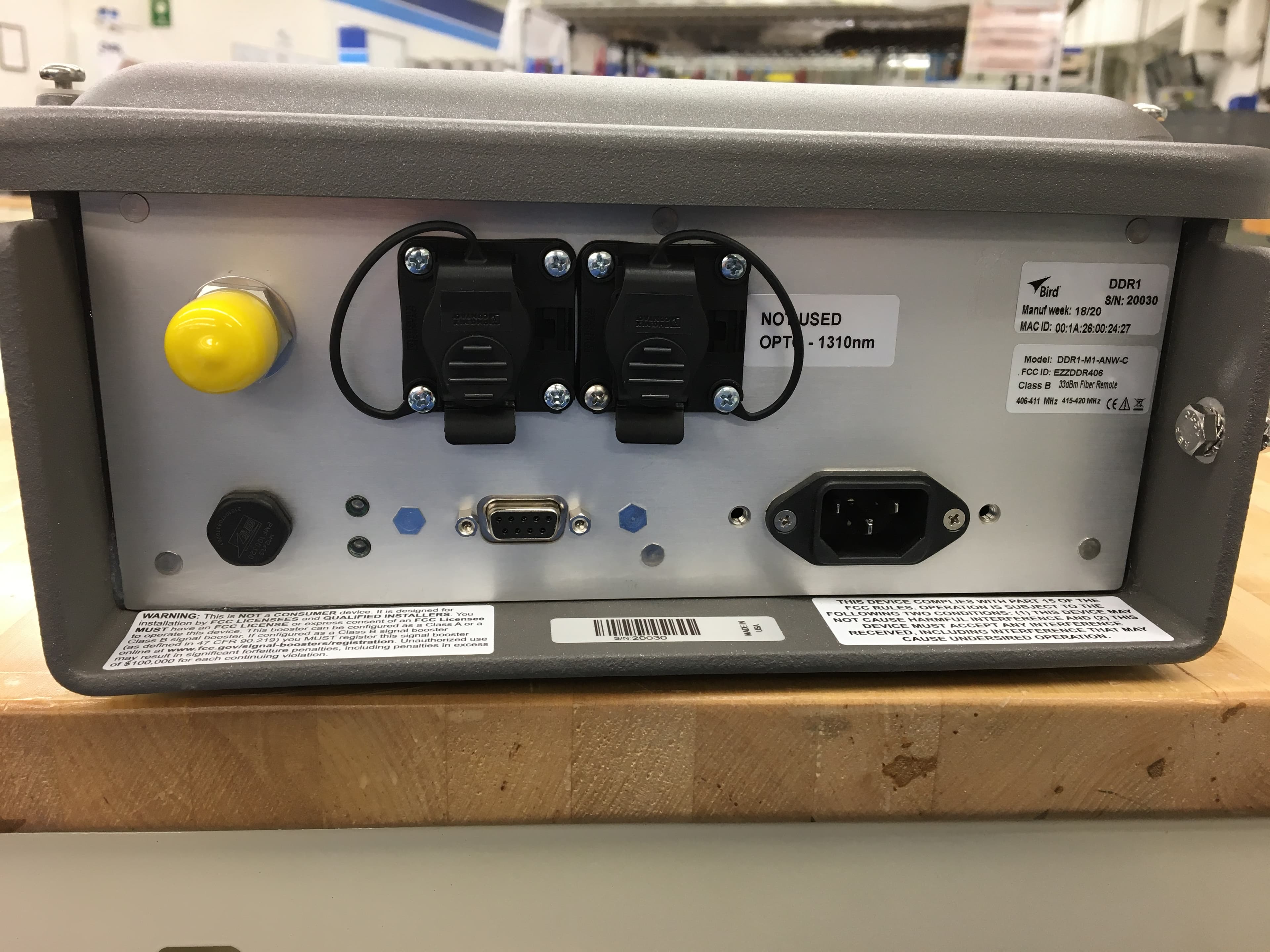
EZZDDR406
Jun 24, 2020DDR Low Band UHF Remote
Equipment Class
B9B - Part 90 Class B Industrial Booster (non-SMR)
EZZ61470
May 19, 2015UHF Digital Signal Booster
Equipment Class
B9A - Part 90 Class A Industrial Booster (non-SMR)
EZZ61470A
May 18, 2015UHF Digital Signal Booster
Equipment Class
B9A - Part 90 Class A Industrial Booster (non-SMR)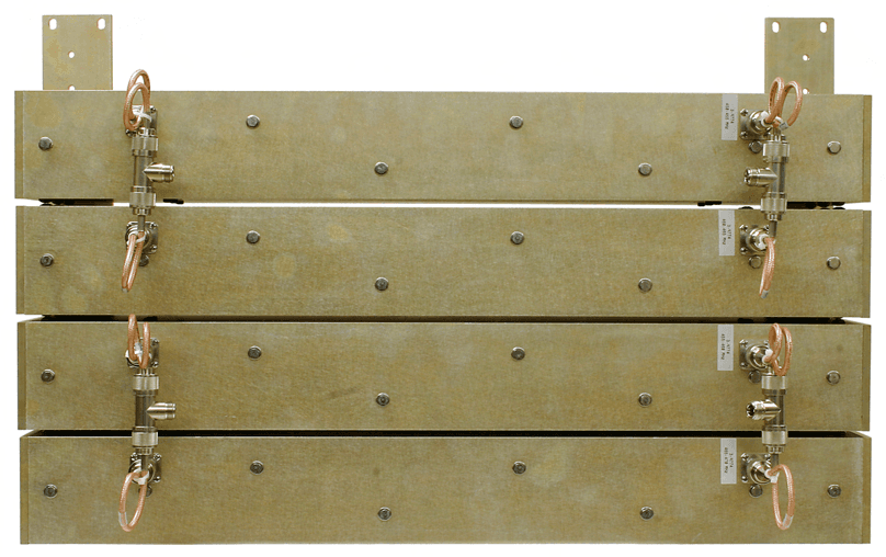
EZZ61170A
Mar 01, 2010Channelized Signal Booster
Equipment Class
TNB - Licensed Non-Broadcast Station Transmitter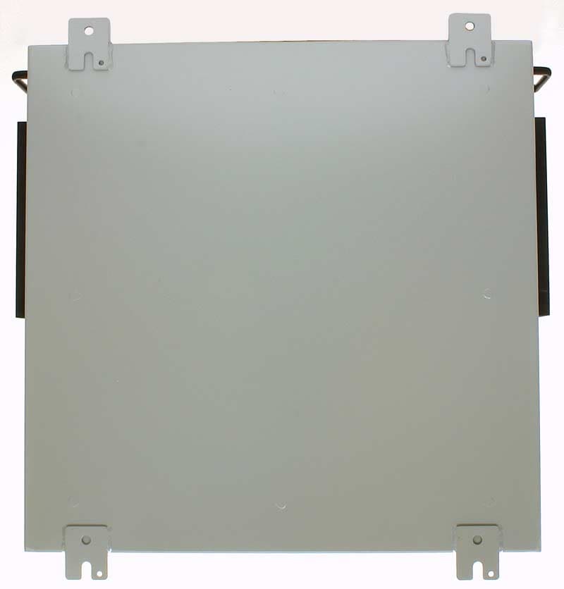
EZZ5PI616550
Sep 21, 2006SIGNAL BOOSTER II (SB II)
Equipment Class
TNB - Licensed Non-Broadcast Station Transmitter