GTC01-9437B574 NETWORK CONTROLLER
Honeywell International Inc.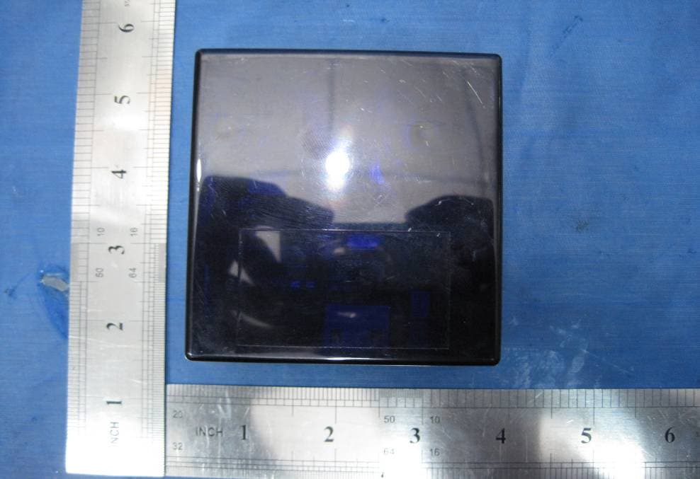
Click to zoom
Application Details
- Equipment Class
- DSS - Part 15 Spread Spectrum Transmitter
- Date of Grant
- Mar 30, 2010
- Application Purpose
- Original Equipment
- Date of Application
- Mar 30, 2010
- Equipment Note
- B574 NETWORK CONTROLLER
- Frequency Range
- 2405.00000000 - 2480.00000000
- Company
- Honeywell International Inc.
- Country
- United States
Documents & Files
Document Text
Text extracted from the exhibit documents filed with the FCC. Open a document above to read the original.
Users Manual
INNCOM B574 Datasheet Overview The INNCOM B574 Network Controller is an INNCOM Integrated Room Automation System (IRAS) product that provides the PAN Coordinator functionality in INNCOM’s Layer-2 802.15.4 Zigbee Mesh network. The B574 serves as the gateway between the wireless routers sending guestroom network data back to the wired network server, where it can be managed by INNCOM’s building management system (INNControl). Features • Supports PoE (Power over Ethernet)[Note: This feature is not currently implemented] • 128 bit AES encryption • Indoor range up to 100ft • 2.4Ghz IEEE 802.15.4 compliant RF transceiver (CC2430 radio core) • Compact physical dimension • DIN Rail mounting option • In general, 50 B574s can be supported in one network segment* Specification Parameter B574 RF Data Rate 250kbps Indoor/Urban range 100ft Transmit Power approximately 10mW Receive Sensitivity -94.6dBm Frequency Band 2.4Ghz Encryption AES-128 Protocol 802.15.4 Frequency Channels 11-26 Network Topology Mesh Maximum per network segment Up to 50* Supply Voltage 12VDC Current Consumption 200mA Operating Ambient Temperature 0-40 ° C Dimensions 86mm x 78mm x 40mm Agency Approvals FCC Part 15, CE Mark ETSI, RoHS *Actual network support may be higher or lower, depending on traffic patterns, selected antenna types, and environmental considerations. Figure 1: B574 INNCOM B574 Datasheet Page | 2 B574 Networking Topology Figure 2: B574 Layer-2 Network Topology The B574 uses ZigBee 802.15.4 technology to create RF Mesh networks. This software-based feature set allows the many network members to link-up in a dynamic way, forming a redundant mesh of routers. A typical router in an INNCOM IRAS is a Layer-2 thermostat or a Layer-2 PC-502. The mesh network is managed by the B574 functioning as the PAN Coordinator. Each B574 can accommodate up to 50 ZigBee routers; each B573 MBX bridge can handle 50 B574 Coordinators. MBX bridges can be added as necessary to accommodate the number of B574s and their routers (50 routers per B574 × 50 B574s per B573 = 2500 routers per B573). (See also the B574 Engineering Manual, v1.0, and the B573 Media Connector Users Guide, v1.0.) The server configures the B574 Coordinator to a selected RF channel and PAN ID on start up. Once it has started a PAN, the coordinator can allow routers in the network to join the PAN. The coordinator transmits and receives RF data transmissions and assists in routing data through the mesh network. In Figure 2 above, data travels along the red route from and to the router on the upper right corner. Should one of the links (hops) break due to a localized disturbance or the failure of a router, then the network would dynamically form another route for the packet; the communication could therefore be maintained even if the network partially fails. INNCOM B574 Datasheet Page | 3 Figure 3 B574 IP Network Topology An IP network based on Ethernet technology serves as the backbone network linking the B574 with the server. The B574 uses a wired Ethernet connection to the B573 (MBX) bridge that communicates with the server using a UDP protocol. In the drawing above, the Layer-2 networks are segregated by PAN ID. Note that the routers in each PAN do not necessarily need to be physically located in geographically segregated locations. If a router can make a solid RF connection into a network, then the router could be geographically located in a neighboring PAN location. INNCOM B574 Datasheet Page | 4 Mechanical Drawings Figure 4: Mechanical Drawings Item Description Part Number 1 Top Housing 53-8084 2 Radio Module 02-9994 3 Main PCBA 02-9845 4 Bottom Housing 53-9918 5 Din Rail Tab 53-9919 Mounting Considerations The B574 Network Controllers are designed for mounting in a variety of applications. The bottom housing is equipped with a channel and tab for DIN rail mounting and therefore does not require any additional screws or hardware for installation. For screw-mounted applications, there are 4 countersunk holes located in the bottom housing that can be accessed by removing the top cover and Printed Circuit Board Assembly (PCBA). INNCOM B574 Datasheet Page | 5 The B574 can be attached to an X-type DIN rail. To attach the B574 to a DIN rail, pull the tab (Figure 5) down and attach the bottom of the housing to the DIN rail (always mount the DIN rail with the tab at the bottom). Once the unit is sitting flush on the rail, release the tab. To remove the B574 from the DIN rail, pull the tab down and lift the bottom edge of the unit off the DIN rail first. This ensures that TAB Figure 5: B574 DIN Rail Installation B574.RF Figure 6: B574 Series DIN Rail Mounted INNCOM B574 Datasheet Page | 6 the cable, cable channels and connections are always aligned in the correct orientation in a daisy- chained application. Figure 7 B574 Top Housing Removal To gain access to headers and connectors located on the PCBA, remove the B574 from the DIN rail or NEMA box enclosure. Using a flat screw driver, lift the top housing away from the snap tangs on the bottom housing. Figure 8 B574 Mounting Screw Locations To screw mount the B574, open the B574 as described above and remove the PCBA. The PCBA is held in place by 4 tangs located at the perimeter of the PCBA. Once the PCBA is removed, locate the 4 countersink posts. Using a self-tapping screw, mount the bottom housing to the intended fixture. Mount the PCBA back on to the bottom housing, make the necessary wire connections (see Headers and Connectors below), connect power to DC jack, plug in Ethernet connection, and then snap the top housing back onto the unit. INNCOM B574 Datasheet Page | 7 Headers and Connections Figure 9 B574 Connections H2 (In System Programming) Pin Function Type Min Max 1-8 Various signals for programming - - - H3 / H4 (S5‐bus In/Out) Pin Function Type Min Max 1-GND Common - - - 2-12VDC Input voltage In 11.75 12.25 3-S5-bus Multi-drop In/Out - - H5 (IR‐Eye) Pin Function Type Min Max 1-GND Common - - - 2-AGC Gain control -…
Text truncated - open the document above for the full version.
Block Diagram
Frequency Range: 2.405-2.480GHz U1 MCU CC2430 X2 Crystal Frequency optional: 32.768K X1 Crystal Frequency: 32MHz +3.3VDC RESETUART_RDUART_TD J1 B574 BLOCK DIAGRAM SERIAL COMMUNICATIONS INTERFACE LOGIC BOARD H7 RADIO BOARD J1 2: +3.3VDC4: RESET6: UART_RD8: UART_TD23/24: GND 2: +3.3VDC4: RF_RESET6: RF_TXD8: RF_RXD23/24: GND REGULATOR +5.0VDC REGULATOR +3.3VDC Input +12VDC Output +12VDC/5VDC/3.3VDC Y1 Crystal Frequency: 16MHz U4 MCU ST72F324J6TX POWER SUPPLY 02-4051 ANT S1 GND +3.3VDC RADIO 02-9994 +12VDC(output)+5.0VDC+3.3VDCGND U1 U2 GND +12VDC(input) TPS54231D TPS62203 GND +3.3VDC H7 GND 1 2 3 4 5 H9ES1 Header Reserved for future use GND +5VDC M24C02 EEPROM U5 1 2 3 4 5 H6ISP Header to program radio 1 2 3 4 5 6 7 8 H2ISP Header to program MCU 12 34 56 78 910 1112 M2POE HEADER RLT8019ASU6 YL18-1064S T1 8 8 7 7 6 6 5 5 4 4 3 3 2 2 1 1 9 9 10 10 Y LED+ 11 Y LED- 12 G LED+ 13 G LED- 14 J3406549-1-ND Y2Crystal Frequency: 20MHz +5VDC GND 1 2 3 4 5 H5IR Eye ‐ M1POWER SUPPLY MODULER HEADER 1 3 2 J112VDC input header 1 2 3 H3S5BUS HEADER 1 2 3 H4S5BUS HEADER GND Ethernet Connectivity +12VDC+5.0VDC+3.3VDCGND D2RED D5AMBER +5VDC RADIO BOARD HEADER +3.3VDC GND GND +12VDC +12VDC +5VDC GND GND +12VDC +5VDC +5VDC GND GND +12VBB +12VDC +12VDC GND GND +12VBB LOGIC BOARD 02-9845
Cover Letter(s)
INNCOM International, Inc FCC ID: GTC01-9437 POWER OF ATTORNEY March.22, 2010 Federal Communications Commission Authorization and Evaluation Division 7435 Oakland Mills Road Columbia, MD 21046 To Whom It May Concern: We, the undersigned, hereby authorize Waltek Services (ShenZhen) Co., Ltd. (Philo Zhong) on our behalf, to apply to the Federal Communications Commission on our equipment. Any and all acts carried out by Waltek Services (ShenZhen) Co., Ltd. (Philo Zhong) on our behalf shall have the same effect as acts of our own. This authorization expires on March.23,2011 This is to advise that we are in full compliance with the Anti-Drug Abuse Act. We, INNCOM International, Inc.are not subject to a denial of federal benefits pursuant to Section 5301 of the Anti-Drug Act of 1988, 21 USC853a, and no party to the application is subject to a denial of federal benefits pursuant to that section. Sincerely, INNCOM International, Inc. .................................... Director of New Product Development
External Photos
2.1 EUT - Front View 2.2 EUT - Back View
ID Label/Location Info
2 FCC ID Label This device complies with Part 15 of the FCC Rules. Operation is subject to the following two conditions:(1)this device may not cause harmful interference,and (2) this device must accept any interference received, including interference that may cause undesired operation. The Label must not be a stick-on paper. The Label on these products must be permanently affixed to the product and readily visible at the time of purchase and must last the expected lifetime of the equipment not be readily detachable. Proposed Label Location on EUT EUT Bottom View/proposed FCC Mark Location FCC ID:GTC01-9437 This device complies with Part 15 of the FCC Rules. Operation is subject to the following two conditions: (1) this device may not cause harmful interference, and (2) this device must accept any interference received, including interference that may cause undesired operation
ID Label/Location Info
FCC ID Label Sample for Model: 01-9437 FCC ID: GTC01-9437 This device complies with Part 15 of the FCC Rules. Operation is subject to the following two conditions: (1)this device may not cause harmful interference, and (2) this device must accept any interference received, including interference that may cause undesired operation.
Internal Photos
2.1 PCB1 - Front View 2.2 PCB1 - Back View 2.3 PCB - Compages View 2.4 PCB2 - Front View 2.5 PCB2 - Back View
Operational Description
B574 CIRCUIT DESCRIPTION APPLICANT: INNCOM International, Inc FCC ID: B574 Assembly 1. B574 includes three modules: logic board 02-9845, power supply 02-4051 and radio module 02-9994. Logic Board 02-9845 1. Power input header and communication interface Header: H3/4: COM, external 12VDC power input, S5 Bus communicates with other devices. J1: External 12VDC power supply input DC jack. 2. S5Bus interface circuit communicates with other devices by bus mode. 3. ISP header H2 used for MCU flash memory in system programming. 16MHz crystal and 15pF load capacitors supply working frequency to MCU U4 ST72F324. Momentary switch S1, amber red D2 and amber D5 are used for MCU diagnostic testing. EEPROM M24C02 is store data by MCU U4 ST72F324. 4. ISP header H6 used for radio module 02-9994 in system programming. Header H7 used to connect radio module 02-9994 to logic board. The interface circuit U7 used for communication between MCU and radio 02-9994. 5. U4 RTL8019AS is a highly integrated Ethernet Controller which offers a simple solution to implement a Plug and Play NE2000 compatible adapter with full-duplex and power down features. 20MHz crystal and 22pF load capacitors supply the working frequency to U4 RTL8019AS. 6. Transformer T1 is a 10 base-T single port magnetic. J3 is an Ethernet socket. 7. Socket M2 is used to connect POE module which provides 12VDC to logic board. POWER SUPPLY MODULE PSH1-L12/02-4052 1. The module 02-4051 is used to transform power supply from 12VDC to 5VDC and 3.3VDC. RADIO MODULE 02-9994 1. MCU CC2430 used to communication with logic board by UART mode. 2. Main frequency: X1, C191 and C211 are used to provide 32MHz frequency to CC2430. Optional frequency: X2, C441 and C431 are used to provide 32.768KHz frequency to CC2430. 3. 2.4GHz RF signal is transmitted and received by the microstrip balun.
Schematics
11 22 33 44 55 66 D D C C B B A A Author: 1 Revision Date:Print Date: Revision: 2 ECO: Disclaimer: 2009-11-23 B574 Logic PCBA02-9845 Ravi Sagar/John Zhang10/14/2009 OF F0 (C) Copy right. Confidential property of INNCOM Inc. SCH_02-9845_F0_P1.SCH Cann ot op en fi le T: \D epartment s\R&D\Parts\SCH Ref Designs\Templa t e\SCH\ Al tiu m Tl ih 68 kR15 15 0 R16 0.1uF C8 S5 RX/TX 12VDC + GND COM 12345 IR-EYEH5 12 VAGC IR5 TX FB60 0 120 6B4 FB60 0 120 6 B13 FB600 B12 FB60 0 120 6 B11 FB600 B10 FB600 B9 IR5 RX 5.6V Z3 10 0kR20 15 0 R22 1.5M R11 98 14 +- LM339U3:3 1110 13 +- LM339 U3:4 10 kR19 33 0pF C11 15 0 R24 IR5 AGC 10 kR10 47nF X7R C10 68 kR3 IRRxIRTx AG C 12 KR14 15 VZ2 10 kR2 312 J1 5.6V Z1 4.7kR21 76 1 +- LM339U3:2 54 2 312 +- LM339 U3:1 Notes:1. All c hip re sistors and ca pa citors are 060 3 unle ss noted. 4.7kR23 33 k R17 +12V D2 S1 4.7kR18 123 S5H4 123 S5H3 FB60 0 120 6B5FB60 0 120 6B8 Vref=2 .5V Vref=2 .5V 12345 ES 1H9 18 0 R41 18 0 R42 5.6VZ6 5.6V Z7 15 pFC16 ICP DATA xRE SE T ICP SELE CTICP CLOCK 15 pFC17 22 0p F C9 OSC1 +5V 47R5 FB600 B3 +5V A0 1 A1 2 VDD 8 VSS 4 SCLK 6 SDAT 5 A2 3 TE ST 7 EE PROMM24C02-MN6 U5 10 KR13 10 KR12 0. 1u F C5 12345678 ISP H2 +12V PE1 1 PE0 44 PD4 11 PA4 34 PC0 23 PD5/ 12 VSS_0 22 PB0 2 PB1 3 PB2 4 PB3 5 PB4 6 PD0 7 PD1 8 PD2 9 PD3 10 VAREF 13 VSSA 14 PF0 15 PF1 16 PF2 17 PF4 18 PF6 19 PF7 20 VDD_0 21 PC1 24 PC2 25 PC3 26 PC4 27 PC5 28 PC6 29 PC7 30 PA3 31 VD D_ 1 32 VSS_1 33 PA5 35 PA6 36 PA7 37 VPP/ICCSEL 38 RESET 39 VSS_2 40 OSC2 41 OSC1 42 VDD_2 43 ST72F324BJ6T6U4 SCL SDA RESERVEDRESERVED ICP DATAICP CLOCK 39 0 R4 10 k R8 ISP = In System Programing 0. 01 uF C18 0. 1u FC7 PE1 3.3k R9 AG CA0A1PB1S5_RxA4A2A3 RF RXD A0 A1A3 A2 A4 S5_Tx RF TXD D3D2D1D0D5D7 RF RST R_RSTDRV R_IOWB R_IORB RESERVED IRTx IRRx LED +5V PB1 D6 D4 15 VZ8 16 MHz Y1 +12V +5V +5V +5V+5V +5V RED S5_Rx S5_Tx 33 pF C37 +12V_VIN IR5RXIR5TX S5 BUS+12VCOM 0. 1u F C4 0. 1u F C6 +5V COM+12VS5BUSSCLKSDAT S5Bus S5Bus TP1 TP2 TP3 TP4 TP5 TP8 D5 3.3k R43 +5V AMBER LED 1 Solder 02-4052 Power Supply Module +5V +12V_VIN +3. 3V (SOURCE) (SOURCE) +12V (SOURCE) S5 BUS+12VCOM 5.6V Z4 5.6V Z5 +12V_BUS VCC_MCU GN D_ BU S GN D 4 GN D 5 +3. 3V DC 6 +5V DC 7 +12V DC 8 EN ABLE 1 VIN 2 GN D 3 PSH 1- L12 MODU LE_ 02 -40 52M1 11 22 33 44 55 66 D D C C B B A A Author: 2 Revision Date:Print Date: Revision: 2 ECO: Disclaimer: 2009-11-23 B574 Logic PCBA02-9845 Ravi Sagar/John Zhang10/14/2009 OF F0 (C) Copy right. Confidential property of INNCOM Inc. SCH_02-9845_F0_P2.SCH Cann ot op en fi le T: \D epartment s\R&D\Parts\SCH Ref Designs\Templa t e\SCH\ Al tiu m CLK2 CLKI BEA D_1 80 6 B14 1. 0M R26 10 K R31 20 0 R27 20 .0 00 0MHz Y2 22 pF C20 22 pF C19 + 10 uF C28 1n F C21 TPOU T+ 45 TPOU T- 46 TPIN+ 59 TPIN- 58 X1 50 X2 51 A0 5 A1 7 A2 8 A3 9 A4 10 A5 11 A6 12 A7 13 A8 15 A9 16 A1 0 18 A1 1 19 A1 2 20 A1 3 21 A1 4 22 A1 5 23 A1 6 24 A1 7 25 A1 8 26 A1 9 27 D0 36 D1 37 D2 38 D3 39 D4 40 D5 41 D6 42 D7 43 D8 95 D9 94 D1 0 93 D1 1 92 D1 2 91 D1 3 90 D1 4 88 D1 5 87 INT0 4 INT1 3 INT2 2 INT3 1 INT4 10 0 INT5 99 INT6 98 INT7 97 AE N 34 IOCHRDY 35 IOCS16B 96 IORB 29 IOWB 30 RSTDRV 33 MEMRB 31 MEMWR 32 CD+ 54 CD- 53 RX+ 56 RX- 55 TX + 49 TX - 48 LE DBNC 60 LE D0 61 LE D1 62 LE D2 63 BA14 74 BA15 73 BA16 72 BA17 71 BA18 69 BA19 68 BA20 67 BA21 66 BD0 85 BD1 84 BD2 82 BD3 81 BD4 80 BD5 79 BD6 78 BD7 77 BCSB 75 EE CS 76 AU I 64 JP 65 VD D 6 VD D 17 VD D 47 VD D 57 VD D 70 VD D 89 GN D 14 GN D 28 GN D 44 GN D 52 GN D 83 GN D 86 RLT8 01 9A S U6 10 K R30 10 K R29 A0A1A2A3A4D0D1D2D3D4D5D6D7 0. 1u F C23 0. 1u F C24 0. 1u F C25 0. 1u F C26 CK1R 0. 1u F C27 1n FC22 1n F 1K V C32 1n F 1K V C30 1n F 1K V C31 GN DE 10 K R37 10 K R38 3. 3K R34 3. 3K R35 3. 3K R33 +3. 3V 36 K R39 15 K R40 +5V 76 1 LM33 9AU7 :2 98 14 LM33 9AU7 :3 1110 13 LM33 9AU7 :4 +5V 0. 1u F C29 Vref=1 .5V Vref=1 .5V RF_RESE T_N ,DTRRF_TxDRF_RxD 1 2 3 4 5 6 7 8 9 10 11 12 13 14 15 16 17 18 19 20 21 22 23 24 Radi o H eader H7 10 K R36 54 2 312 LM33 9AU7 :1 Vref=1 .5V RF_RTSRF_CTS RF_ICP_DataRF_ICP_Clock RF_RESE T_N NCNCNCNCNCNCNCNCNC NC NCNCNCNC 12345 H6 +3. 3V RF_ICP_DataRF_ICP_ClockRF_RESET_N +5V 1 2 3 4 5 6 7 8 9 10 11 12 POE HeaderM2 CT1CT2 SP1SP2 A0A1A2A3 D0D1D2D3D4D5D6D7 A4 +5V +5V -1 +5V-1 +5V-1 R_IORBR_IOWB R_RSTDRV RF RSTRF TXDRF RXD +12VBB +12VBB UN USED Header to Program Radio TP9 TP1 0 8 8 7 7 6 6 5 5 4 4 3 3 2 2 1 1 9 9 10 10 Y LED+ 11 Y LED- 12 G LED+ 13 G LED- 14 40 65 49 -1-NDJ3 TD + 1 TCT 2 TD - 3 NC 4 NC 5 RD+ 6 RCT 7 RD- 8 RX- 9 RXCT 10 RX+ 11 NC 12 NC 13 TX - 14 TX CT 15 TX + 16 YL18-1064ST1 10 0n F C1 0. 1u F C2 LA N_L ED1 3. 3kR28 LA N_L ED0 3. 3kR1 +5V+5V LA N_L ED1LA N_L ED0 FB60 0 120 6B1 +12V_VIN FB60 0 120 6B2 GN D Title: Size Document Number: REV Sheet of Zigbee TXR.SMT PCBA 02-9994 INNCOM INTERNATIONAL, INC C O N F I D E N T I A L D1 9994D.SCH 11 Date of Revision: Feb 16, 2009 Printed on: 16-Feb-2009 Assembly Number: 02-9994 Orcad B DVDD 7 P1_3 5 P1_4 4 P1_5 3 P1_6 2 P1_7 1 P1_0/LED 9 P1_2 6 P1_1/LED 8 RESET_N 10 P0_0 11 P0_1 12 P0_2 13 P0_3 14 P0_4 15 P0_5 16 P0_6 17 P0_7 18 XOSC_Q2 19 AVDD_SOC 20 XOSC_Q1 21 RBIAS1 22 AVDD_RREG 23 RREG_OUT 24 AVDD_IF1 25 RBIAS2 26 AVDD_CHP 27 VCO_GUARD 28 AVDD_VCO 29 AVDD_PRE 30 AVDD_RF1 31 RF_P 32 TXRX_SWITCH 33 RF_N 34 AVDD_SW 35 AVDD_RF2 36 AVDD_IF2 37 AVDD_ADC 38 DVDD_ADC 39 AVDD_DGUARD 40 AVDD_DREG 41 DCOUPL 42 P2_4/XOSC_Q2 43 P2_3/XOSC_Q1 44 P2_2 45 P2_1 46 DVDD 47 P2_0 48 GND 49 U1 CC2430 C471100nF C71100nF C411220nF C207100nF VDD GND GND GND GND GND GND GND GND C38168pF C35110nF C281100nF C27168pF C25168pF GND GND GND GND GND GND GND GND GND GND L33122nH 5% X2 32.768K X1 32M R26143k R2412 C241220nF C231220nF VDD C19122pF C21122pF C44115pF C43115pF C34115pF GND 1 2 3 4 5 6 7 8 9 10 11 12 13 14 15 16 17 18 19 20 21 22 23 24 J1 PINROW_2*12 P2.0/JOY_PUSHP2.1/DDP2.2/DCP1.0/LED1P1.1/LED2P1.2/VDD_SW_CTRLP1.3/GPIOP1.4/CSn/SS/CTSP1.5/SCLK/RTSP1.6/SI/MOSI/UART_TDP1.7/SO/MISO/UART_RDP0.0/Radio_ID0P0.1/BUTTON_PUSHP0.2/EE_SDAP0.3/EE_SCLP0.4/ACC_XP0.5/ACC_YP0.6/Radio_ID1P0.7/Radio_ID2RESET_N VDD R10143K VDDGND P0.…
Text truncated - open the document above for the full version.
Test Report
INNCOM International, Inc FCC ID: GTC01-9437 FCC TEST REPORT Page 1 of 45 Ref No.:WT10030687-E-E-F FCC ID : GTC01-9437 Applicant : INNCOM International, Inc Address of Applicant : 277 West Main Street Niantic, CT 06357 United States of America. Equipment Under Test (EUT) : Product description : B574 Network Controller Model No. : 01-9437 Frequency Range : 2405~2480MHz Standards : FCC 15 Paragraph 15.247 Date of Test : March.24,2010 Test Engineer : Olic huang Reviewed By : PERPARED BY: Waltek Services (Shenzhen) Co., Ltd. 1/F, Fukangtai Building,West Baima Rd.,Songgang Street, Baoan District, Shenzhen 518105,China Tel :+86-755-27553488 Fax:+86-755-27553868 INNCOM International, Inc FCC ID: GTC01-9437 Page 2 of 45 Ref No.:WT10030687-E-E-F 2 Contents Page 1 COVER PAGE..........................................................................................................................................................1 2 CONTENTS ..............................................................................................................................................................2 3 TEST SUMMARY....................................................................................................................................................4 4 GENERAL INFORMATION..................................................................................................................................5 4.1 CLIENT INFORMATION............................................................................................................................................5 4.2 GENERAL DESCRIPTION OF E.U.T...........................................................................................................................5 4.3 DETAILS OF E.U.T. .................................................................................................................................................5 4.4 DESCRIPTION OF SUPPORT UNITS...........................................................................................................................5 4.5 STANDARDS APPLICABLE FOR TESTING..................................................................................................................5 4.6 TEST FACILITY........................................................................................................................................................6 4.7 TEST LOCATION......................................................................................................................................................6 4.8 EQUIPMENT USED DURING TEST.............................................................................................................................7 5 CONDUCTED EMISSION TEST ........................................................................................................................10 5.1 TEST EQUIPMENT..................................................................................................................................................10 5.2 TEST PROCEDURE.................................................................................................................................................10 5.3 CONDUCTED TEST SETUP.....................................................................................................................................11 5.4 EUT OPERATING CONDITION...............................................................................................................................11 5.5 CONDUCTED EMISSION LIMITS.............................................................................................................................12 5.6 CONDUCTED EMISSION TEST DATA......................................................................................................................12 5.7 CONDUCTED EMISSION TEST SETUP VIEW............................................................................................................14 6 RADIATION EMISSION TEST...........................................................................................................................15 6.1 TEST EQUIPMENT..................................................................................................................................................15 6.2 MEASUREMENT UNCERTAINTY.............................................................................................................................15 6.3 TEST PROCEDURE.................................................................................................................................................15 6.4 RADIATED TEST SETUP.........................................................................................................................................16 6.5 SPECTRUM ANALYZER SETUP...............................................................................................................................16 6.6 CORRECTED AMPLITUDE & MARGIN CALCULATION............................................................................................17 6.7 SUMMARY OF TEST RESULTS................................................................................................................................17 6.8 EUT OPERATING CONDITION...............................................................................................................................18 6.9 RADIATED EMISSIONS LIMIT ON PARAGRAPH 15.209 ...........................................................................................18 6.10 RADIATED EMISSIONS TEST RESULT................................................................................................................19 6.11 RADIATED EMISSION DATA.............................................................................................................................19 7 MAXIMUM PEAK OUTPUT POWER...............................................................................................................24 8 HOPPING CHANNEL NUMBER.…
Text truncated - open the document above for the full version.
Test Setup Photos
2 Photographs of Testing Radiation Emission Test View For 30MHz-1000MHz Radiation Emission Test View For 1GHz-25GHz Conducted Emission Test Setup View
Contact Information
Applicant
Jeanne Enaux(Sr. Quality Engineering Manager)
Test Firm
Waltek Services(Shenzhen) Co., Ltd.Philo zhong
Technical Specifications
| # | Rule Parts | Frequency Range | Power Output |
|---|---|---|---|
| 1 | 15C | 2.40 GHz - 2.48 GHz | 8.00 mW |
Other Applications from Honeywell International Inc.
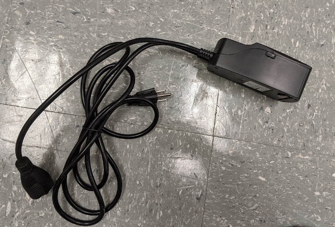
GTC-201705X
Mar 22, 2021L510 Lamp Controller
Equipment Class
DTS - Digital Transmission System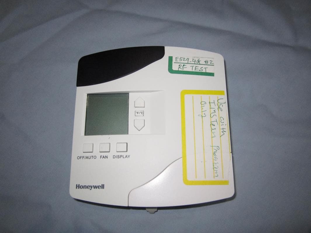
GTC202153TXR
Aug 27, 2014Battery Powered Thermostat
Equipment Class
DXX - Part 15 Low Power Communication Device Transmitter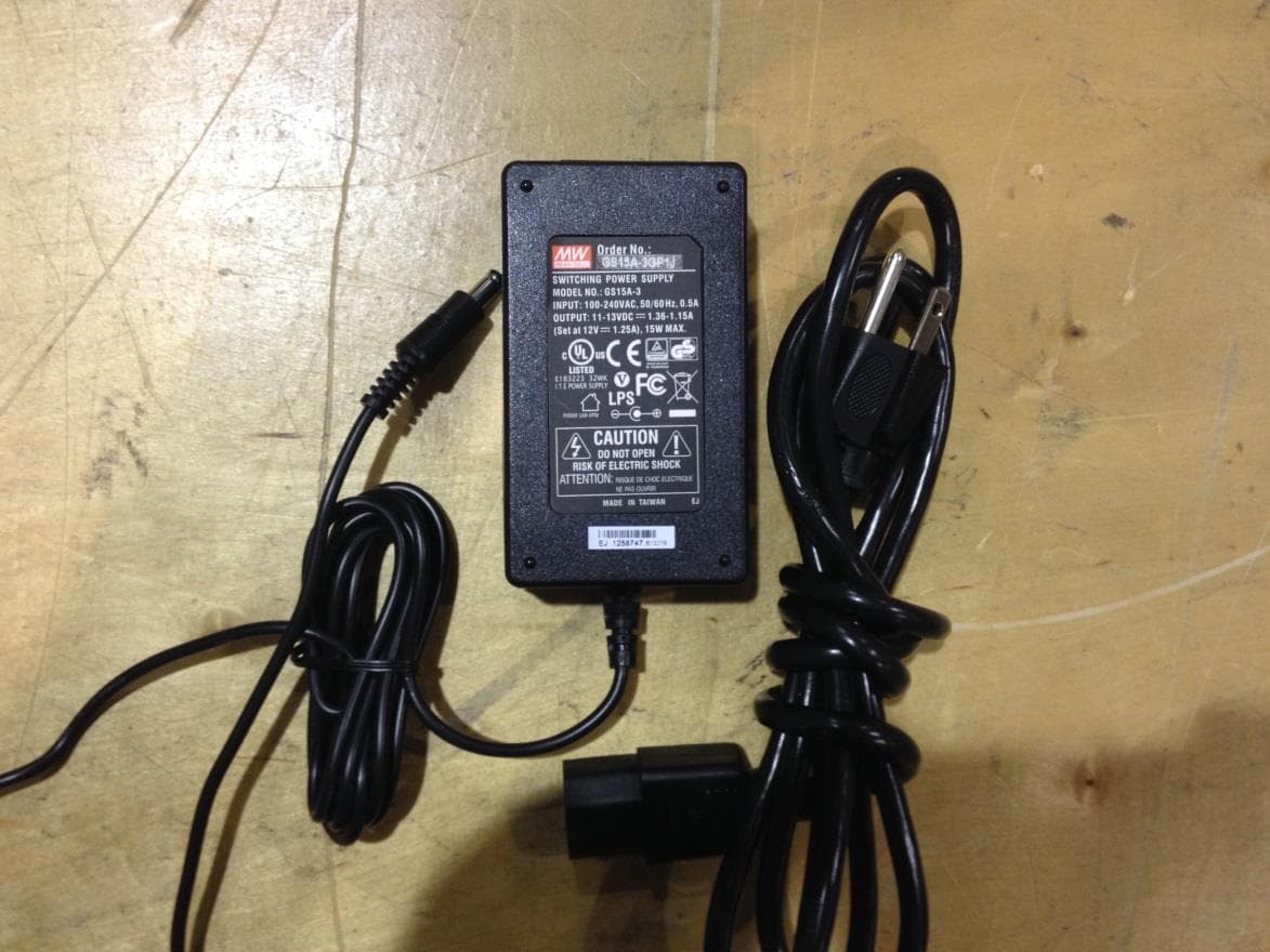
GTC201104TXR
Aug 26, 2014B578 Ethernet to RF Protocol Converter
Equipment Class
DXX - Part 15 Low Power Communication Device Transmitter
GTC202125TXR
Aug 17, 2014Wireless Repeater Module
Equipment Class
DTS - Digital Transmission System
GTC202124TXR
Sep 18, 2013Repeater
Equipment Class
DXX - Part 15 Low Power Communication Device Transmitter