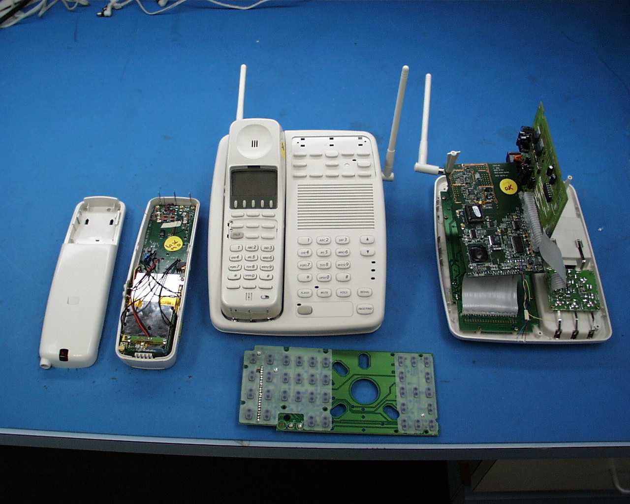
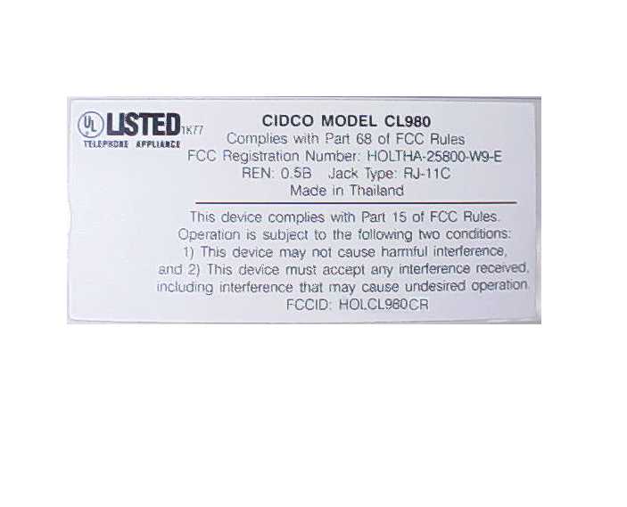
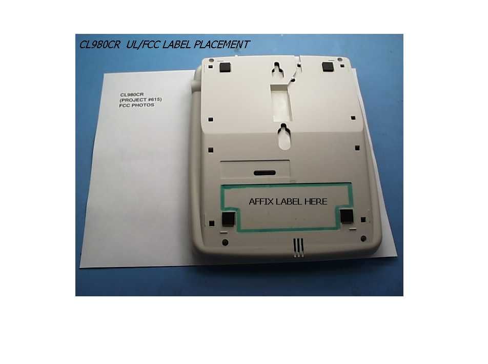
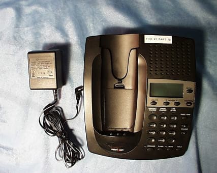
HOLCL980CRCordless Telephone Base Unit
Cidco Communications Corporation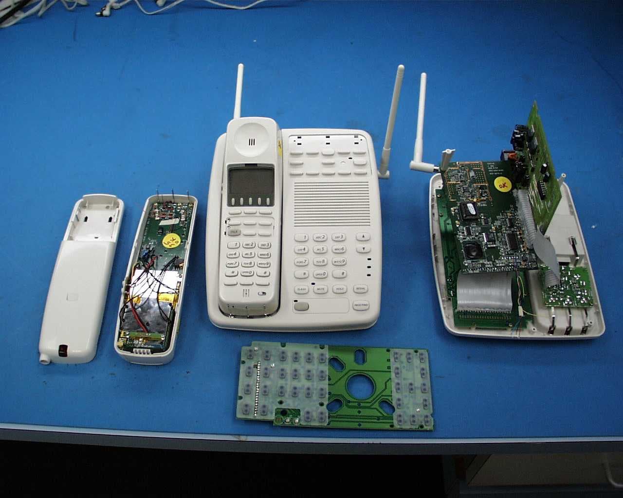
Click to zoom
Application Details
- Equipment Class
- DSS - Part 15 Spread Spectrum Transmitter
- Date of Grant
- Dec 16, 1999
- Application Purpose
- Original Equipment
- Date of Application
- Aug 19, 1999
- Equipment Note
- Cordless Telephone Base Unit
- Frequency Range
- 904.20000000 - 925.80000000
- Country
- United States
Documents & Files
Document Text
Text extracted from the exhibit documents filed with the FCC. Open a document above to read the original.
Users Manual
TITLE: DOC NO. REVISION SHEET 1 OF : : : E-mail address: [email protected] Contact________________ Phone___________ Fax___________ Modem________________ Fold qWrap-around q FINISH Collate qSlip sheet q Staple q Drill qScore qPerf q Saddle stitch q Perfect q PMS _______ Wire O qGBC q Spot color q INK Black q BINDING Color separations q SPECIAL INSTRUCTIONS DATE Text stock______________ Sample attached qFinished size ________ 1 Sided q2 Sided q Cover stock____________ Insert stock_______________ PA P E R Color _______ Text stock (Asia)______________ or Engineering Approved Equivalent FILM/FILES CHECKED BY:________________________________________________ DATE:__________________________________________________________________ : SOURCE Film q Adobe PDF o CL980-01 English and Spanish Manual 102230-01 A Jeanine Healy (408) 778-8061 (408)776-2631 (408)776-8063 jeanine.healy 60 lb glossy self-cover 108 g x 5.5X8.5 289 x X PDF provided for Document Control. 1 set of film for the factory. 06/16/99 3 Jeanine Healy 05/16/99 x x TITLE: DOC NO. REVISION SHEET OF : : 2 102230-01 A 3 CL980-01 (CIDCO logoed) coverFCCTOCCopyrightGetting to know Setting Up Yo u r Phone Personalizi ng Your Phone Diagram Using Your Phone Using the Directory Using Yo u r Custom Trouble- shooting Index IndiceIndex Resolucio n de problemas iiiiiiiv1234 5678910 1112 1314151617181920 2122232425262728 2930313233343536 3738394041424344 4443424140393837 TITLE: DOC NO. REVISION SHEET OF : : 2 102230-01 A 3 CL980-01 (CIDCO logoed) Como usar los servicios blank Uso del Directorio Como Usar Su telefono Instalacion su de telefono Conozca su neevo telefono ContenidoFCCSpanish cover 3635343332313029 2827262524232221 2019181716151413 12111098765 4321iviiiiii CL-980 CL-980 CL-980 CORDLESS TELEPHONE CORDLESS TELEPHONE CORDLESS TELEPHONE REPLAY BACK PLAY FWD SKIP 3-WAY CALL CALL RETURN REPEAT DIAL ON OFF ERASE MSG SAVE MSG VOICE MAIL LINE IN USE INTERCOM CHARGE 7 PQRS 8 TUV 9 WXYZ FLASH MUTE HOLD REDIAL 0 OPER # 4 GHI 5 JKL 6 MNO VOLUME 1 ABC 2 3 DEF SPEAKERPHONE PAGE/FIND CALLERS SEND TO VM DIRECTORY CALL BACK INTERCOM HOLD MEMORY 3-WAY DIAL FLASH 9:18 9:16 18 AM PM LINE 1 & LINE 2 408 - 555-1212 SMITH JOHN CALL DIR 1 2 ABC 3 DEF FLASH HOLD REDIAL ON OFF—RING DELETE REVIEW VOICE MAIL 3-WAY REPEAT DIAL CALL CALL FWD. TALK 4 GHI 5 JKL 6 MNO 7 PRS 8 TUV 9 WXY 0 OPER # PWR—ON OFF CALL FORWARD Cidco980.book Page 1 Thursday, June 3, 1999 6:39 PM This equipment has been tested and found to comply with the limits for a Class B digital device, pursuant to Part 15 of the FCC Rules. These limits are designed to provide reasonable protection against harmful interference in a residential installa- tion. This equipment generates, uses, and can radiate radio frequency energy, and if not installed and used in accordance with the instructions, may cause harmful in- terference to radio communications. However, there is no guarantee that interfer- ence will not occur in a particular installation. If this equipment does cause harmful interference to radio or television reception, which can be determined by turning the equipment off and on, the user is encouraged to try to correct the interference by one or more of the following measurements: qReorient or relocate the receiving antenna. qIncrease the separation between the equipment and receiver. qConnect the equipment into an outlet on a circuit different from that to which the receiver is connected. qConsult the dealer or an experienced radio/TV technician for help. !CAUTION Changes or modification to this device not expressly approved by CIDCO Inc. could void the user’s authority to operate this equipment. Cover.fm Page 2 Tuesday, June 15, 1999 11:20 AM TABLE OF CONTENTS qTABLE OF CONTENTS 3 qGETTING TO KNOW YOUR NEW PHONE 1 qU NPACKING YOUR PHONE 1 qL OCATING KEYS, LIGHTS, AND SWITCHES 2 qSETTING UP YOUR PHONE 5 qP ERSONALIZING YOUR PHONE 7 qE ASY SETUP 8 qD ETAILED SETUP 10 qUSING YOUR PHONE 17 qU SING TRADITIONAL DIALING 17 qU SING PRE-DIALING 17 qU SING SPEED DIALING 18 qA NSWERING CALLS 18 qU SING FLASH 21 qU SING MUTE 21 qU SING THE SPEAKERPHONE 22 qA DJUSTING THE VOLUME 22 qU SING HOLD 23 qT IMING CALLS 23 qG ETTING TEMPORARY TONE SERVICE 23 qG OING OUT OF RANGE 23 qL OCATING A LOST HANDSET 23 qU SING THE INTERCOM 24 qR EADING DISPLAY MESSAGES 24 qUSING THE DIRECTORY 27 qC REATING YOUR DIRECTORY LIST 27 qE NTERING CHARACTERS & SYMBOLS 29 qD IALING FROM DIRECTORY RECORDS 30 qR EVIEWING DIRECTORY RECORDS 30 Cidco980.book Page 3 Thursday, June 3, 1999 6:39 PM Table of Contents qDELETING DIRECTORY RECORDS 31 qMAINTAINING BATTERIES 31 qUSING YOUR CUSTOM CALLING SERVICES 32 q3-W AY CALLING 32 qC ALL FORWARDING 32 qC ALL RETURN 33 qC ALL WAITING 34 qC ALLER ID AND CALL WAITING ID 34 qR EPEAT DIALING 36 qV OICE MAIL 37 qTROUBLESHOOTING 38 qINDEX 41 Copyright © 1998-99 by CIDCO Incorporated. All rights reserved. ©1998 CIDCO Incorporated. No part of this publication may be reproduced, transcribed, stored in a retrieval system, or translated into any language in any form, by any means, without the written permission of CIDCO Incorporated. Patents pending. 102230-01 Rev A Cidco980.book Page 4 Thursday, June 3, 1999 6:39 PM Getting to Know Your New Phone 1 GETTING TO KNOW YOUR NEW PHONE Your new CL980 telephone incorporates all the best features of a cordless tele- phone and blends them with your local telephone company’s best calling features, such as Caller ID, Voice Mail and Call Waiting ID. If this is your first cordless telephone, you’ll soon discover that your cordless is sim- ilar to regular telephones, except without the cord. If you’ve owned a cordless in the past, you’ll discover that the CL980 telephone is the most powerful and full- function Caller ID cordless telephone on the market. Some key features are: q20 channel, digital spread spectrum 900 MHz handset with speakerphone q50 Caller ID memory and 50 Directory Records qDedicated Voice Mail keys qLarge One Time Viewing (OTV ® ) display qHearin…
Text truncated - open the document above for the full version.
Operational Description
220 Cochrane Circlepage 1 of 2 Morgan Hill, CA 9503756644 DATE: JULY 29, 1999 TO:SHARI MEYERSPHONE:(410) 354 - 3300 MET LABORATORIES, INC. FAX:(410) 354 - 3313 FROM:TERRY KILLIONDIRECT:(408) 778 - 8016 SENIOR MEMBER OF TECHNICAL STAFFMAIN:(408) 779 - 1162 WIRELESS COMMUNICATIONS DESIGN GROUPFAX:(408) 776 - 2631 [email protected] RE:CL980CR, CL990, CL940 FCC MODIFICATION FILING CC:RON ANGLIKOWSKI, S.A. FOO, CAN TRI NGUYEN This is a request to submit a modification filing for the CIDCO CL980CR, CL990, and CL940 model cordless telephones. The three models mentioned above are part of a product family of CIDCO 900MHz Digital Spread Spectrum Cordless Telephones which support Caller ID and Voicemail functions. They are derived from the original CIDCO CL980 Cordless Telephone, see figure 1. A brief description for each model is provided below. CL980CR: The CIDCO CL980CR is a cost reduced version of the original CIDCO CL980 Cordless Telephone. The reason for modification from the CL980 is purely for cost reduction and improved RF performance. The base “RF” platform was changed from the Conexant “Skyhawk” to the Conexant “Hummingbird” chipset. All functionality and overall user interface remains the same. The cordless telephone is a full featured 900MHz Direct Sequence Spread Spectrum cordless telephone which supports Caller ID, Call Waiting ID, Voicemail, and Call Disposition. It also includes a half-duplex speakerphone with base set/handset intercom. The handset is designed with a backlit display to view Caller ID and Directory records and the base set includes a spare battery charge compartment. 220 Cochrane Circlepage 2 of 2 Morgan Hill, CA 9503756644 CL990: The CIDCO CL990 is an enhanced version of the CL980CR Cordless Telephone. It has all of the features of the CL980CR except for the addition of a backlit LCD on the base set for viewing and managing CALLER ID information. One row of repertory keys was also removed from the base set to accommodate the extra space required for the LCD. CL940: The CIDCO CL940 is a feature-reduced version of the CL980CR. The following features were removed to create a basic version 900MHz Digital Spread Spectrum cordless telephone. The CL940 does not include the following features found on the CL980CR; • "Dial-In" Base • Speakerphone • Intercom • Spare Battery Charger • Base "Voicemail" keys • Base "Repertory" keys • Base "Dial" keys CIDCO 900MHz DSS CORDLESS TELEPHONE OVERVIEW: The CL980CR establishes a baseline for this CIDCO Cordless Telephone product family. From there a higher end product was developed which included an additional backlit LCD located on the base set, which gives the user the ability to monitor incoming calls and also manage CALLER ID and Directory records from the base set. Another lower end product was developed from the CL980CR, which eliminated many of the functions found on the base set to reduce cost. The idea was to have a product line to target the low, medium, and high end markets. All three cordless telephones operate from the same hardware and software platform. It is because of this commonality that we would like to treat this submission as a modification rather than a new filing. By: _______________________ ___________________________ Signed Printed Date: _______________________ Title: _______________________
Test Report
FCC ID: HOLCL980CR August 26, 1999 Federal Communications Commission Authorization and Evaluation Division 7435 Oakland Mills Road Columbia, MD 21046 Attention:Applications Examiner Reference:FCC ID: HOLCL980CR CIDCO Model CL980CR Cordless Telephone Base Unit Dear Examiner: The following equipment authorization application is presented on behalf of CIDCO , Inc. for the certification of their Model CL980CR Cordless Telephone Base unit. Enclosed, please find complete data and documentation package demonstrating that this device complies with the technical requirements of 47 CFR, Part 15, Subpart C for an Intentional Radiator. The manufacturer seeks authorization under the FCC ID: HOLCL980CR. We look forward to an expeditious review of the report presented and a granting of the certification for CIDCO , Inc. If you have any questions or we can be of assistance, in this matter, please call us at (410) 354-3300. Best regards, Chris Harvey EMC Laboratory Director, MET Laboratories, Inc. Enclosures FCC ID: HOLCL980CR August 24, 1999 - 2 - EM IU9544B MET Laboratories, Inc. Safety Certification - EMI - Telecom Environmental Simulation 914 WEST PATAPSCO AVENUE !! BALTIMORE, MARYLAND 21230-3432 !! PHONE (410) 354-3300 !! FAX (410) 354-3313 ENGINEERING TEST REPORT in support of the Application for Grant of Equipment Authorization EQUIPMENT: Model CL980CR Cordless Telephone Base Unit FCC IDENTIFIER:HOLCL980CR SPECIFICATION:15.247(a) thru (e); 15.209(a). Manufacturer:CIDCO , Inc. 220 Cochrane Circle Morgan Hill, CA 95037 TESTING DATE(S):24, 25, 26 May, and 24 July 1999 MANUFACTURER'S REPRESENTATIVE: Mr. Can Nguyen ENGINEERING STATEMENT I ATTEST: the measurements shown in this report were made in accordance with the procedures indicated, and that the emissions from this equipment were found to be within the limits applicable. I assume full responsibility for the accuracy and completeness of these measurements, and for the qualifications of all persons taking them. ______________________ Alvin Ilaraia Test Engineer, MET Laboratories, Inc. FCC ID: HOLCL980CR August 24, 1999 - 3 - EM IU9544B MODIFICATIONS STATEMENT I ATTEST: that the product will be manufactured with all modifications for Part 15 compliance as submitted in this report. Modifications made during testing appear below: 1. No modifications were made to the EUT. 1.0 INTRODUCTION The following test report is presented on behalf of the Applicant , as verification of the compliance of the CIDCO Direct Sequence, Spread -Spectrum Telephone Base unit , Model: CL980CR. 2.0 TEST SITE All testing was conducted at MET Laboratories, Inc., 914 West Patapsco Avenue, Baltimore, Maryland 21230-3432. Radiated emissions measurements were performed on a three-meter open air test site (OATS). A complete site description is on file with the FCC Laboratory Division as 31040/SIT/MET. 3.0 TEST EQUIPMENT USED ManufacturerEquipment Calibration DueCal. Interval Hewlett Packard8593EM Spectrum Analyzer12/1/99annual EMCOXwing Antenna 11454/1/00annual EMCOActive Rod Antenna2/15/00annual EMCODouble Ridge Horn 311511/18/99annual EMCOLISN 3825/24/3/00annual 4.0 TEST CONFIGURATION The CIDCO Cordless Telephone Base model CL980CR , was configured with the Model: CL9HS Handset in accordance with the manufacturer's instructions and operated in a manner representative of the typical usage of the equipment. During testing of the EUT, the Base unit Model # CL980CR was manipulated within the confines of typical usage to maximize each emission. FCC ID: HOLCL980CR August 24, 1999 - 4 - EM IU9544B 6.0 TEST TYPE(S) 6.1As required by §15.247(b) of CFR 47, output power measurements radiated measurements were performed to verify compliance with the conducted limit. 6.2As required by §15.247(a)(2) of CFR 47, 6 dB bandwidth measurements were performed 6.3 As required by §15.247(e) of CFR 47, processing gain Measurements were not performed. Data is provided instead, by the spread spectrum chipset manufacturer 6.4As required by §15.247(c)(1 )& (c)(2) of CFR 47, out of band emissions measurements were performed. 6.5As required by §15.247(d) of CFR 47, power density measurements were performed 6.6As required by §15.107 of CFR 47, Line Conducted Emission measurements were performed FCC ID: HOLCL980CR August 24, 1999 - 5 - EM IU9544B Equipment:Base Station (900MHz Cordless Telephone) Model #:CL980CR Serial #:not provided FCC ID:HOLCL980CR Equipment:Handset (900MHz cordless Telephone) Model #:CL9HS Serial #:not provided FCC ID:HOLCL9HS Equipment:CO simulator Model #:MET Labs 1.5m unshielded RJ-11 cable Serial #:n/a FCC ID #:n/a 7.0 EUT CONFIGURATION INFORMATION FCC ID: HOLCL980CR August 24, 1999 - 6 - EM IU9544B Photograph(s) of Radiated Emissions Test Configuration CIDCO Model CL980CR Cordless Telephone FCC ID: HOLCL980CR August 24, 1999 - 7 - EM IU9544B Photograph(s) of Line Conducted Emissions Test Configuration CIDCO Model CL980CR Cordless Telephone Base FCC ID: HOLCL980CR August 24, 1999 - 8 - EM IU9544B SUBJECT:Peak Output PowerMET REPORT:EM9544B 15.247(b)MFG:CIDCO FCC Part 15, Subpart CTESTED BY:Ken Bass Intentional RadiatorTEST DATE(S):25 May 1999 EUT:CIDCO MODEL:CL980CR (Telephone Base unit ) TECHNICAL SPECIFICATION:15.247(b) CARRIER POWER:Peak Output power was calculated through the following means: The raw reading from the analyzer was added to the cable loss and antenna factor (for the specific frequency of measurement). The final E-field strength limit is derived from the conversion of the power limit specified in FCC Part. 15.247(b) to V/m , considering a 50S system. Please see the attached plots Handset/FreqWorst caseDist (m)Cbl/HPF/CPreCorrTotal Total Base (GHz)Raw+ACFonamplevel(V/m)watts ReadingLoss(dB)(dBμV/m) (dBuV/m)(dB) Base914.76109.503.02.8*n/a112.400.389 0.045 * - Cable losses only. No High-pass filter (i.e. insertion loss) factors, etc., associated with measurement. The Model CL980CR system results for the Base are provided as the highest level of the system. (Across the enti…
Text truncated - open the document above for the full version.
Test Report
Processing Gain Measurements for Rockwell’s DCT 1. Introduction 1.1 Scope This document is a Rockwell Semiconductor Systems (RSS) Engineering report. This document details the results of measurement of the processing gain of a DCT FFF phone. 1.2 Intended Readers The intended readers of this document are RSS marketing, application, engineering, test engineering, technical publication, and management personnel. This document is not intended for distribution outside of RSS. 1.3 Reference Documents This section lists documents that are referenced within or are materially relevant to this document. Code of Federal Regulations, Title 47, Chapter 1, Part 15 Radio Frequency Devices (FCC) 1.4 Definitions FCCFederal Communications Commission SNRSignal to Noise Ratio JSRJammer to Signal Ratio CWContinuous wave (jammer) HSHandset BSBasestation DBPSKDifferential Binary Phase Shift Keying Table 1: Definitions and Abbreviations 2. An Overview of the FCC Method for measuring Processing Gain Two methods are specified for measuring processing gain by the FCC in 15.247 (e). The first method simply involves calculating the signal to ratio noise (SNR) with the spreading code switched on with the SNR when the spreading code is switched off. The difference between the two is the processing gain. The SNR is measured at the demodulated output of the receiver. In principle this an acceptable method to measure the processing gain of any direct sequence spread spectrum communication system, however, it does not take into consideration that the non-spread spectrum portion of the system may operate under the assumption that the signal being transmitted is a spread spectrum signal and when the spreading code is switched off the system may fail to operate or operate at greatly reduced efficiency, In either case the measurement of processing gain will be meaningless. The second method specified by the FCC to measure processing gain is detailed in 15.247 (e)(1). This involves transmitting a CW jammer in the RF passband of the system and measuring the jammer to signal ratio (JSR) required to achieve a certain bit error rate. The choice of the actual value of the bit error rate is left up to the tester. The jammer is stepped in 50 kHz increments across the entire passband and in each case the JSR to achieve the desired bit error rate is measured. The JSR is measured at the RF input to the system under test. The lowest 20% of the JSR data (in dB) is discarded. The processing gain can then be calculated as follows:- system measuredtheory p L S J N S G+ ö ç è æ + ÷ ö ç è æ = where G p is the processing gain, the SNR is that theoretically predicted for the system under the test to achieve the desired bit error rate, the JSR is the lowest value (in dB) in the remaining data set and L sys adjusts for non-ideal system losses. L sys can not be greater than 2 dB. 3. Processing Gain Measurement Results The following parameters were used in the test setup. HS Tx power (dBm)-1.9 BS LNA gain (dB)0 Channel attenuation (dB)-50 Test system losses (signal) (dB) -11.75-4.05 dB (system), -6 dB (signal combiner), -1.7 dB (2 cables) Test system losses (jammer) (dB) -12.85-12 dB (signal combiner), -0.85 dB (cable) Table 2: Test Setup Parameters The following measurement results were taken at the basestation. The desired bit error rate was set at 10 -3 . Jammer Frequency (MHz) BER (BS)Received jammer power (dBm) Received signal power (dBm) Jammer/Signal ratio (dB) 913.80 9.4×10 -4 -59.55-63.654.1 913.85 9.6×10 -4 -57.95-63.655.7 913.90 9.6×10 -4 -60.15-63.653.5 913.95 9.6×10 -4 -64.25-63.65-0.6 914.00 1.1×10 -3 -61.55-63.652.1 914.05 9.8×10 -4 -61.55-63.652.1 914.10 1.1×10 -3 -61.95-63.651.7 914.15 9.2×10 -4 -62.85-63.650.8 914.20 1.0×10 -3 -59.85-63.653.8 914.25 1.0×10 -3 -61.15-63.652.5 914.30 1.1×10 -3 -62.05-63.651.6 914.35 1.0×10 -3 -57.65-63.656.0 914.40 1.1×10 -3 -55.65-63.658.0 914.45 1.0×10 -3 -49.35-63.6514.3 914.50 1.1×10 -3 -59.25-63.654.4 914.55 1.0×10 -3 -62.35-63.651.3 914.60 9.7×10 -4 -59.05-63.654.6 914.65 1.0×10 -3 -61.05-63.652.6 914.70 1.1×10 -3 -62.55-63.651.1 914.75 9.0×10 -4 -61.95-63.651.7 914.80 1.0×10 -3 -61.05-63.652.6 914.85 9.9×10 -4 -62.35-63.651.3 914.90 1.1×10 -3 -64.05-63.65-0.4 914.95 9.2×10 -4 -56.25-63.657.4 915.00 1.0×10 -3 -59.85-63.653.8 915.05 1.1×10 -3 -57.25-63.656.4 915.10 9.9×10 -4 -58.15-63.655.5 Table 3: Test Results Figure 1: Test Setup For DBPSK at 10 -3 bit error rate the required SNR is 8.0 dB. Using the results above and the data in the table below the processing gain is calculated to be 11.3 dB. required SNR (dB)8.0 system losses (dB)2.0 J/S ratio at 80% point (dB)1.30 FCC Processing gain (dB)11.3 Table 4: Processing Gain Calculation data 4. Conclusions The result measured for processing gain of 11.3 dB is close to the actual processing gain due to a 12 chip spreading code of 10 × log 10 (12) = 10.8 dB Signal Combiner -6 dB cable (-0.85 dB) RF Attenuator (-50 dB) cable (-0.85 dB) RF Signal generator (HP8663A) -12 dB cable (-0.85 dB) additional system loss (-4.05 dB) (voice signal only)
Test Report
Processing Gain Measurements for Conexant’s DCT 1. Scope This document details the results of measurement of the processing gain of a DCT FFF phone with reference to the Code of Federal Regulations, Title 47, Chapter 1, Part 15 Radio Frequency Devices (FCC). FCCFederal Communications Commission SNRSignal to Noise Ratio JSRJammer to Signal Ratio CWContinuous wave (jammer) HSHandset BSBasestation DBPSKDifferential Binary Phase Shift Keying Table 1: Abbreviations 2. An Overview of the Processing Gain Processing Gain Calculation Theoretical processing gain limit for the 12bit Spreading BPSK system is 10.8dB. Processing Gain = 10 Log (Spreaded data rate / Unspreaded data rate) = 10 Log [(12 Chip/bit * 100Kbit/sec) / 100 Kbit/sec)] = 10 Log [12] = 10.8 dB Processing Gain Measurement Method Following method is specified by the FCC to measure processing gain. The detailed are in FCC documents 15.247 (e)(1). This involves transmitting a CW jammer in the RF passband of the system and measuring the jammer to signal ratio (JSR) required to achieve a certain bit error rate. The choice of the actual value of the bit error rate is left up to the tester. The jammer is stepped in 50 kHz increments across the entire passband and in each case the JSR to achieve the desired bit error rate is measured. The JSR is measured at the RF input to the system under test. The lowest 20% of the JSR data (in dB) are discarded. The processing gain can then be calculated as follows: - system measuredtheory p L S J N S G+ + = where G p is the processing gain, the SNR is that theoretically predicted for the system under the test to achieve the desired bit error rate, the JSR is the lowest value (in dB) in the remaining data set and L sys adjusts for non-ideal system losses. L sys can not be greater than 2 dB. 3. Processing Gain Measurement Test Setup The following parameters were used in the test setup. HS Tx power (dBm)-1.9 BS LNA gain (dB)0 Channel attenuation (dB)-50 Test system losses (signal) (dB) -11.75-4.05 dB (system), -6 dB (signal combiner), -1.7 dB (2 cables) Test system losses (jammer) (dB) -12.85-12 dB (signal combiner), -0.85 dB (cable) Table 2: Test Setup Parameters Signal Combiner -6 dB cable (-0.85 dB) RF Attenuator (-50 dB) cable (-0.85 dB) RF Signal generator (HP8663A) -12 dB cable (-0.85 dB) additional system loss (-4.05 dB) (voice signal only) 4. Results & Calculation The following measurement results were taken at the basestation. The desired bit error rate was set at 10 -3 . Jammer Frequency (MHz) BER (BS)Received jammer power (dBm) Received signal power (dBm) Jammer/Signal ratio (dB) 913.80 9.4×10 -4 -59.55-63.654.1 913.85 9.6×10 -4 -57.95-63.655.7 913.90 9.6×10 -4 -60.15-63.653.5 913.95 9.6×10 -4 -64.25-63.65-0.6 914.00 1.1×10 -3 -61.55-63.652.1 914.05 9.8×10 -4 -61.55-63.652.1 914.10 1.1×10 -3 -61.95-63.651.7 914.15 9.2×10 -4 -62.85-63.650.8 914.20 1.0×10 -3 -59.85-63.653.8 914.25 1.0×10 -3 -61.15-63.652.5 914.30 1.1×10 -3 -62.05-63.651.6 914.35 1.0×10 -3 -57.65-63.656.0 914.40 1.1×10 -3 -55.65-63.658.0 914.45 1.0×10 -3 -49.35-63.6514.3 914.50 1.1×10 -3 -59.25-63.654.4 914.55 1.0×10 -3 -62.35-63.651.3 914.60 9.7×10 -4 -59.05-63.654.6 914.65 1.0×10 -3 -61.05-63.652.6 914.70 1.1×10 -3 -62.55-63.651.1 914.75 9.0×10 -4 -61.95-63.651.7 914.80 1.0×10 -3 -61.05-63.652.6 914.85 9.9×10 -4 -62.35-63.651.3 914.90 1.1×10 -3 -64.05-63.65-0.4 914.95 9.2×10 -4 -56.25-63.657.4 915.00 1.0×10 -3 -59.85-63.653.8 915.05 1.1×10 -3 -57.25-63.656.4 915.10 9.9×10 -4 -58.15-63.655.5 Table 3: Test Results For DBPSK at 10 -3 bit error rate the required SNR is 8.0 dB. Using the results above and the data in the table below the processing gain is calculated to be 11.3 dB. required SNR (dB)8.0 system losses (dB)2.0 J/S ratio at 80% point (dB)1.30 FCC Processing gain (dB)11.3 Table 4: Processing Gain Calculation data Conclusions The result measured for processing gain of 11.3 dB is close to the actual processing gain due to a 12 chip spreading code of 10 × log 10 (12) = 10.8 dB
Test Report
Hummingbird 900MHz System Processing Gain Date: December 12, 1999 1. Scope This document details the results of measurement of the processing gain of a DCT FFF phone with reference to the Code of Federal Regulations, Title 47, Chapter 1, Part 15 Radio Frequency Devices, FCC. The purpose of this document is to provide conceptual background of processing gain and method of measurement. Table 1: Abbreviations FCCFederal Communications Commission SNRSignal to Noise Ratio JSRJammer to Signal Ratio CWContinuous wave (jammer) HSHandset BSBasestation DBPSKDifferential Binary Phase Shift Keying 2. An Overview of the Processing Gain Processing Gain Calculation Theoretical processing gain limit for the 12bit Spreading BPSK system is 10.8dB. Processing Gain = 10 Log (Spreaded data rate / Unspreaded data rate) = 10 Log [(12 Chip/bit * 100Kbit/sec) / 100 Kbit/sec)] = 10 Log [12] = 10.8 dB Processing Gain Measurement Method Following method is specified by the FCC to measure processing gain. The detailed are in FCC documents 15.247 (e)(1). This involves transmitting a CW jammer in the RF passband of the system and measuring the jammer to signal ratio (JSR) required to achieve a certain bit error rate. The choice of the actual value of the bit error rate is left up to the tester. The jammer is stepped in 50 kHz increments across the entire passband and in each case the JSR to achieve the desired bit error rate is measured. The JSR is measured at the RF input to the system under test. The lowest 20% of the JSR data (in dB) are discarded. The processing gain can then be calculated as follows: system measuredtheory p L S J N S G+ + = where G p is the processing gain, the SNR is that theoretically predicted for the system under the test to achieve the desired bit error rate, the JSR is the lowest value (in dB) in the remaining data set and L sys adjusts for non-ideal system losses. L sys can not be greater than 2 dB. 3. Processing Gain Measurement Test Setup The test set up is shown in Fig.1. The base station and handset are configured to measure the Bit Error Rate (BER) through serial ports of a personal computer. Conexant’s software utility program (FCC_3V3.exe) is used to configure the test modes, establish the link between the base and handset unit and monitor the results. The BER test results are displayed on the monitor. The strength of the received signal entering at the receiving antenna port of the unit under test is derived from the signal strength of the transmitting unit. General Procedure Step-1: Measure the output power of the base and handset units in LOW power mode. Step-2: Connect the serial interface of the base and handset to the serial ports of a PC. Step-3: Connect the base and handset through attenuator, signal combiner etc components using 50 ohm SMA connectors and cables as shown in Figure 1. Thus, the BER test set up establishes link through wired connection. Step-4: Using utility test software, select the channel frequency (904.2MHz), LOW power mode, LNA attenuation for base and handset units. Step-5: Click on “Start S7 HS Master” button ON. The two link is established and the BER results are displayed on monitor. Step-6: Feed jamming signal from the signal generator. Step-7: Increase the amplitude of the jamming while monitoring BER such that the BER is ≤ 10E-3. This signal power is recorded for computing received Jammer power level J. Step-8: Increment the Jammer signal frequency in steps of 20kHz and repeat step 7 and determine the minimum Jammer signal power to achieve BER of ≤ 10E-3. Calculate the processing gain. Figure –1: Bit Error Rate (BER) Test Setup The following parameters were used in the test setup. Table 2: Test Setup Parameters HS Tx power (dBm)-1.9 BS LNA gain (dB)0 Channel attenuation (dB)-50 Test system losses (signal) (dB) -11.75-4.05 dB (test setup), -6 dB (signal combiner), -1.7 dB (2 cables) Test system losses (jammer) (dB) -12.85-12 dB (signal combiner), -0.85 dB (cable) Cable (-0.85 dB) RF Attenuator (0 ~ 50 dB) RF Signal Generator (HP8663A) Signal Combiner -6 dB Cable (-0.85 dB) -6 dB Cable (-0.85 dB) 6 dB Attenuator Base Station (Unit under Test) Handset BER Monitor Personal Computer Serial Port-2 Serial Port-1 4. Results & Calculation The following measurement results were taken at the basestation. The desired bit error rate was set at 10 -3 . Table 3: Test Results Jammer Frequency (MHz) BER (BS)Received jammer power (dBm) Received signal power (dBm) Jammer/Signal ratio (dB) 913.80 9.4×10 -4 -59.55-63.654.1 913.85 9.6×10 -4 -57.95-63.655.7 913.90 9.6×10 -4 -60.15-63.653.5 913.95 9.6×10 -4 -64.25-63.65-0.6 914.00 1.1×10 -3 -61.55-63.652.1 914.05 9.8×10 -4 -61.55-63.652.1 914.10 1.1×10 -3 -61.95-63.651.7 914.15 9.2×10 -4 -62.85-63.650.8 914.20 1.0×10 -3 -59.85-63.653.8 914.25 1.0×10 -3 -61.15-63.652.5 914.30 1.1×10 -3 -62.05-63.651.6 914.35 1.0×10 -3 -57.65-63.656.0 914.40 1.1×10 -3 -55.65-63.658.0 914.45 1.0×10 -3 -49.35-63.6514.3 914.50 1.1×10 -3 -59.25-63.654.4 914.55 1.0×10 -3 -62.35-63.651.3 914.60 9.7×10 -4 -59.05-63.654.6 914.65 1.0×10 -3 -61.05-63.652.6 914.70 1.1×10 -3 -62.55-63.651.1 914.75 9.0×10 -4 -61.95-63.651.7 914.80 1.0×10 -3 -61.05-63.652.6 914.85 9.9×10 -4 -62.35-63.651.3 914.90 1.1×10 -3 -64.05-63.65-0.4 914.95 9.2×10 -4 -56.25-63.657.4 915.00 1.0×10 -3 -59.85-63.653.8 915.05 1.1×10 -3 -57.25-63.656.4 915.10 9.9×10 -4 -58.15-63.655.5 For DBPSK at 10 -3 bit error rate the required SNR is 8.0 dB. Using the results above and the data in the table below the processing gain is calcu…
Text truncated - open the document above for the full version.
Contact Information
Applicant
Ron Anglikowski(Engineering Director)
Technical Contact
MET Laboratories, Inc.Ken Bass
[email protected]410-354-3300
914 West Patapsco Ave. · Baltimore, Maryland · United States
Non-Technical Contact
MET Laboratories, Inc.Terri Wolf
[email protected]410-354-3300
Test Firm
MET Laboratories, Inc.John Mason
Technical Specifications
| # | Rule Parts | Frequency Range | Power Output |
|---|---|---|---|
| 1 | 15C | 904.2 MHz - 925.8 MHz | 45.00 mW |
Other Applications from Cidco Communications Corporation
HOLE272
Jun 25, 20032.4GHz DSS Cordless Telephone
Equipment Class
DTS - Digital Transmission System
HOLD93X
Oct 06, 2002900MHz Digital Spread Spectrum Cordless Phone
Equipment Class
DTS - Digital Transmission System
HOLCL906
Jun 27, 2002900MHz Cordless Telephone System
Equipment Class
DXT - Part 15 Low Power Transceiver, Rx Verified
HOLD933
May 12, 2002900MHz DSS Cordless Telephone System
Equipment Class
DSS - Part 15 Spread Spectrum Transmitter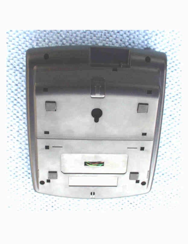
HOLD271
Mar 07, 20022.4GHZ Spread Spectrum Cordless Telephone
Equipment Class
DSS - Part 15 Spread Spectrum Transmitter