IHET5DK1SC4812T-MC @ 800 MHz CDMA BTS
Nokia Solutions and Networks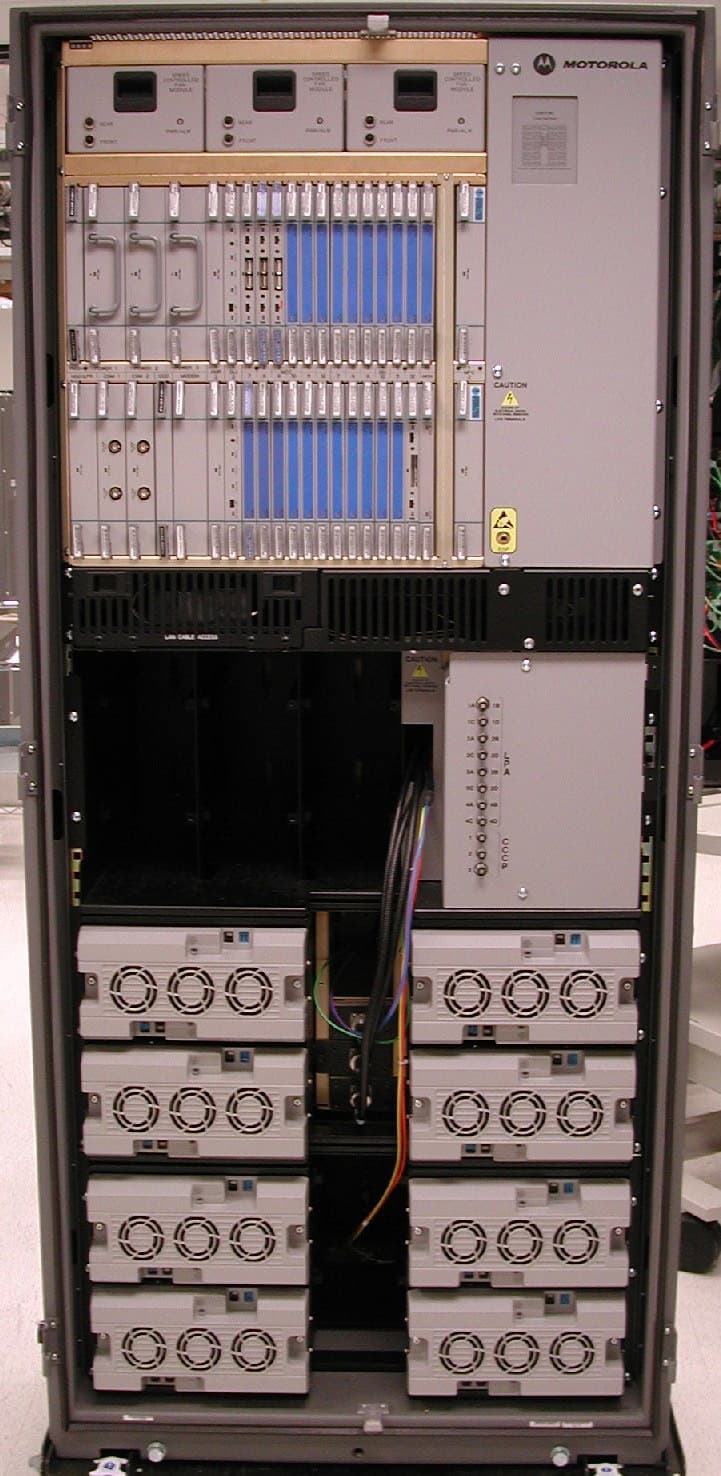
Click to zoom
Application Details
- Equipment Class
- TNB - Licensed Non-Broadcast Station Transmitter
- Date of Grant
- May 08, 2003
- Application Purpose
- Original Equipment
- Date of Application
- May 08, 2003
- Equipment Note
- SC4812T-MC @ 800 MHz CDMA BTS
- Frequency Range
- 869.70000000 - 893.31000000
- Company
- Nokia Solutions and Networks
- Country
- United States
Documents & Files
Document Text
Text extracted from the exhibit documents filed with the FCC. Open a document above to read the original.
Users Manual
CONTROLLED INTRODUCTION 68P64115A19–4 Mar 2003 ENGLISH CDMA Software Release R2.16.1.x Technical Information 1X SC 4812T-MC BTS Hardware Installation 800 MHz CONTROLLED INTRODUCTION SPECIFICATIONS SUBJECT TO CHANGE WITHOUT NOTICE Notice While reasonable efforts have been made to assure the accuracy of this document, Motorola, Inc. assumes no liability resulting from any inaccuracies or omissions in this document, or from use of the information obtained herein. The information in this document has been carefully checked and is believed to be entirely reliable. However, no responsibility is assumed for inaccuracies or omissions. Motorola, Inc. reserves the right to make changes to any products described herein and reserves the right to revise this document and to make changes from time to time in content hereof with no obligation to notify any person of revisions or changes. Motorola, Inc. does not assume any liability arising out of the application or use of any product, software, or circuit described herein; neither does it convey license under its patent rights or the rights of others. It is possible that this publication may contain references to, or information about Motorola products (machines and programs), programming, or services that are not announced in your country. Such references or information must not be construed to mean that Motorola intends to announce such Motorola products, programming, or services in your country. Copyrights This instruction manual, and the Motorola products described in this instruction manual may be, include or describe copyrighted Motorola material, such as computer programs stored in semiconductor memories or other media. Laws in the United States and other countries preserve for Motorola certain exclusive rights for copyrighted material, including the exclusive right to copy, reproduce in any form, distribute and make derivative works of the copyrighted material. Accordingly, any copyrighted Motorola material contained herein or in the Motorola products described in this instruction manual may not be copied, reproduced, distributed, merged or modified in any manner without the express written permission of Motorola. Furthermore, the purchase of Motorola products shall not be deemed to grant either directly or by implication, estoppel, or otherwise, any license under the copyrights, patents or patent applications of Motorola, as arises by operation of law in the sale of a product. Usage and Disclosure Restrictions License Agreement The software described in this document is the property of Motorola, Inc. It is furnished by express license agreement only and may be used only in accordance with the terms of such an agreement. Copyrighted Materials Software and documentation are copyrighted materials. Making unauthorized copies is prohibited by law. No part of the software or documentation may be reproduced, transmitted, transcribed, stored in a retrieval system, or translated into any language or computer language, in any form or by any means, without prior written permission of Motorola, Inc. High Risk Activities Components, units, or third–party products used in the product described herein are NOT fault–tolerant and are NOT designed, manufactured, or intended for use as on–line control equipment in the following hazardous environments requiring fail–safe controls: the operation of Nuclear Facilities, Aircraft Navigation or Aircraft Communication Systems, Air Traffic Control, Life Support, or Weapons Systems (“High Risk Activities”). Motorola and its supplier(s) specifically disclaim any expressed or implied warranty of fitness for such High Risk Activities. CONTROLLED INTRODUCTION SPECIFICATIONS SUBJECT TO CHANGE WITHOUT NOTICE Trademarks and Motorola are registered trademarks of Motorola, Inc. Product and service names profiled herein are trademarks of Motorola, Inc. Other manufacturers’ products or services profiled herein may be referred to by trademarks of their respective companies. Copyright 2003 Motorola, Inc. Printed on Recyclable Paper REV012501 SC 4812T-MC vs SC 4812T BTS Read Me First (Comparison) 68P64115A19–4 Mar 20031X SC 4812T-MC BTS Hardware Installation - Software Release R2.16.1.x CONTROLLED INTRODUCTION RMF-1 Read Me First SC 4812T-MC vs SC 4812T BTS Read Me First (Comparison) This Read-me-first document describes a summary of changes between the existing SCt4812T BTS and the SC 4812T-MC (Multicarrier) BTS. The SC 4812T-MC is based on the existing SC 4812T platform and employs similar hardware and architecture. The differences between these products are briefly described and illustrated below. This section is not intended to replace the SC 4812T-MC manual set. Multicarrier provides the capability for all PAs in all quadrants to provide trunked power across all sector/carriers. This differs from the previous architecture in which PA modules within a quadrant provided trunked power to only one carrier. Furthermore, in SC 4812T-MC, adjacent channels can be combined onto one antenna versus being transmitted on separate antennas in SC 4812T. An overview of the BTS differences is illustrated in the following table and in illustrations on the following pages (Figure 1 thru Figure 4). SC 4812T Description#DescriptionSC 4812T-MC 1 2 3x3 DC Power Input (see Figure 1) 1 2x2 DC Power Input (see Figure 1) 1 2 7 3 I/O Plate supporting 3x3 DC Power Input (see Figure 2) 2 I/O Plate supporting 2x2 DC Power Input (see Figure 2) 3 4 CCCP Fan Tray 3 CCCP Speed Controlled Fan Tray 4 C-CCP Cage: SCIO (3- or 6-Sector) SBBX-1X SSwitch 4 C-CCP Cage: SMCIO (3- or 6-Sector) SHigh Power BBX-1X SHigh Power Switch 6 5 PA Shelves: SSC 4812T LPA S4x4 TX Backplane SPA Location and Mapping (see Figure 3) 5 PA Shelves: SSC 4812T CLPA SMulticarrier module SParallel PA Combiner SEnhanced Trunking Module SLPA/PLC Filler Panel SPA Location and Mapping (see Figure 3) 5 6 7 2:1 or 4:1 Combiners or Dual Bandpass TX Filters 6 TX Bandpass Filters and/or TX Output Termi…
Text truncated - open the document above for the full version.
Block Diagram
m Global Telecom Solutions Sector SC4812T-MC @ 800 MHz CDMA BTS FCC ID: IHET5DK1 Block Diagram Exhibit M 4/29/2003 11:02 AM Global Telecom Solutions Sector, 5555 North Beach Street TX14-7C, Fort Worth, Texas Telephone (817) 245-6039, Fax (817) 245-6248, Email [email protected] 12 12 12RX Main 12 TX 12RX Div High Power LPAs + Trunking Modules MCC1X HP BBX1X (Redundant) HP Switch Power Supply CDMA Clock Distribution Clock Synch Module MPC3 Span IO High Stability Oscillator C-CCP Shelf GLI2 AMR GPS RX Filters 6 or 12 6 or 12 6 or 12 Clk/Sync 2 12 12 Filter / Combiner Filter / Combiner if 3 sector 3 TCH Data13 Fwd13 Rvs CT1 SpanTo/From CBSC 3 6 RX TX Optional Comm / Bus Clk / Sync RF 2 2 Customer Alarms Site IO LAN In / Out To LMF HP BBX1X CIO Rx Rx Tx Tx Remote GPS Dist Optional Frame Block Diagram
External Photos
m Global Telecom Solutions Sector SC4812T-MC @ 800 MHz CDMA BTS FCC ID: IHET5DK1 External Photo Exhibit M 4/29/2003 10:14 AM Global Telecom Solutions Sector, 5555 North Beach Street TX14-7C, Fort Worth, Texas Telephone (817) 245-6039, Fax (817) 245-6248, Email [email protected] Photo Number Photograph Description Page 1 Front View with Doors Closed 2 2 Front View with Doors Open 3 3 Rear View with Panel 4 4 Rear View without Panel 5 5 Left Side View 6 6 Right Side View 7 7 Top View 8
ID Label/Location Info
m Global Telecom Solutions Sector SC4812T-MC @ 800 MHz CDMA BTS FCC ID: IHET5DK1 FCC Identification Nameplate/Frame Label Location Exhibit M 4/29/2003 10:28 AM Global Telecom Solutions Sector, 5555 North Beach Street TX14-7C, Fort Worth, Texas Telephone (817) 245-6039, Fax (817) 245-6248, Email [email protected] EQUIPMENT NAMEPLATE PER CFR., Title 47, Part 2.925 Bar Coding Graphics to be black A name plate of this type, or one similar to it, will be affixed to every base station. This label is permanent, indelible, and tamper evident. || | |||| | ||| | |||||| | | ||||| ||| ||| || | | |||||| Serial No. Complies with Part 68, FCC Rules Model No. _____________ ||||| | | ||| |||| ||||| | | | ||||| | |||| ||| || || || | | FCC Reg. No. REN: USOC: MOTOROLA FCC ID: IHET5DK1 m Global Telecom Solutions Sector SC4812T-MC @ 800 MHz CDMA BTS FCC ID: IHET5DK1 FCC Identification Nameplate/Frame Label Location Exhibit M 4/29/2003 10:30 AM Global Telecom Solutions Sector, 5555 North Beach Street TX14-7C, Fort Worth, Texas Telephone (817) 245-6039, Fax (817) 245-6248, Email [email protected]
Internal Photos
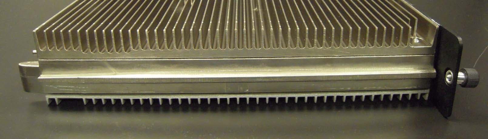
m Global Telecom Solutions Sector SC4812T-MC @ 800 MHz CDMA BTS FCC ID: IHET5DK1 Internal Photo Exhibit M 5/2/2003 10:30 AM Global Telecom Solutions Sector, 5555 North Beach Street TX14-7C, Fort Worth, Texas Telephone (817) 245-6039, Fax (817) 245-6248, Email [email protected] Photo Number Photograph Description Part Page 1 HP BBX 1X Front with cover 1 of 3 2 2 HP BBX 1X Front without cover 1 of 3 3 3 HP BBX 1X Back 1 of 3 4 4 CCD Front with cover 1 of 3 5 5 CCD Front without cover 1 of 3 6 6 CCD Back 1 of 3 7 7 CIO Front 1 of 3 8 8 CIO Back 1 of 3 9 9 CSM Front 1 of 3 10 10 CSM Back 1 of 3 11 11 GLI Front 2 of 3 1 12 GLI Back 2 of 3 2 13 HSO Front 2 of 3 3 14 HSO Back 2 of 3 4 15 LFR Front 2 of 3 5 16 LFR Back 2 of 3 6 17 CLPA Front 2 of 3 7 18 CLPA without cover 2 of 3 8 19 CLPA Back 2 of 3 9 20 MCC 1X Front 2 of 3 10 21 MCC 1X Back 2 of 3 11 22 MPC3 Front 2 of 3 12 23 MPC3 Back 2 of 3 13 24 RGD Front 3 of 3 1 25 RGD Back 3 of 3 2 26 SITE I/O Front 3 of 3 3 27 SITE I/O Back 3 of 3 4 28 SPAN I/O Front 3 of 3 5 29 SPAN I/O Back 3 of 3 6 30 HP Switch Card Front 3 of 3 7 31 HP Switch Card Back 3 of 3 8 32 PS Front 3 of 3 9 33 PS Back 3 of 3 10 34 FTM Front 3 of 3 11 35 FTM Back 3 of 3 12
Operational Description
SC4812T-MC @ 800 MHz CDMA BTS FCC Filing 1 DESCRIPTIVE INFORMATION FCC FILING FOR SC4812T-MC @ 800 MHz CDMA BTS The Information in this exhibit is in accordance with the FCC Rules and Regulations, Vol. II, Part 2, Subpart J. Sections 2.1033 through 2.1055 are addressed. Section 2.1033 (a) Name of Applicant and Manufacturer: MOTOROLA Section 2.1033 (b) Identification of Equipment: IHET5DK1 Section 2.1033 (c) Quantity Production: Quantity Production is Planned. Section 2.1033 (d) Technical Description This Transmitter is intended for use in the Public Cellular Radio Telecommunications Service and is designed in compliance with the FCC Rules and Regulations Title 47, Part 22(H).This transmitter is capable of spread spectrum (CDMA) operation per IS2000 standard Walsh codes to support Pilot, Sync, Paging and Traffic channels. (1) Types of Emissions This equipment will be capable of operation using wide band spread spectrum techniques employing Direct Sequence Code Division Multiple Access (DS-CDMA) digital communication techniques. For this transmitter, the emission designator is 1M30F9W (per FCC Part 2.201, subpart C). (2) Frequency Range This transmitter operates within the 869.70 to 893.31 MHz Band (per FCC Part 22). This base station will support CDMA operations on channel numbers 1013 through 1023 and 1 through 777 inclusive. (3) Range of Operating Power The rated maximum average power out of the SC4812T-MC @ 800 MHz CDMA BTS is 120 W (50.8 dBm) per carrier. However, in CDMA the actual power output is based on the number of traffic channels in operation. The minimum power occurs when only a pilot signal is present. The maximum power occurs when a pilot along with synchronization, paging, and traffic channels are present. SC4812T-MC @ 800 MHz CDMA BTS FCC Filing 2 (3) Range of Operating Power (cont.) For a typical system setup, the theoretical difference between minimum power and maximum power is 8dB. The output power is variable in 0.25 dB steps. The range is 12 dB. In addition, the dynamics of a CDMA system allow for what is called “cell breathing”. This allows an operator to vary the range of a cell by controlling the power of the pilot signal. (4) Maximum Power Limits The peak output power of a base station transmitter may not exceed 500 Watts as defined in Part 22.913 (a) (5) Applied voltages and currents into the final transistor elements of the transmitter output: The applied voltages and currents into each of the Linear Power Amplifier’s final transistor elements are as follows: Drain 27.0 VDC Drain Current 1.0 AMPS Gate Voltage 4 VDC (6) Function of Each Active Device Refer to the Operational Description Exhibit. (7) Complete Circuit Diagrams Refer to the Schematics Exhibit. (8) Instruction/Installation Manual Refer to the Installation Manual Exhibit. (9) Tune-Up/Optimization Procedure Refer to the Installation Manual Exhibit. SC4812T-MC @ 800 MHz CDMA BTS FCC Filing 3 (10) Means for Frequency Stabilization Refer to the Test Report Exhibit. The Clock Synchronization Module (CSM/CSM2) provides clock and time signals for an SC4812T-MC @800 MHz CDMA BTS. In addition, it provides the primary source, a 3 MHz clock, for the transmit synthesizer in the Broadband Transceiver. The CSM/CSM2 relies on a GPS receiver, either riding piggyback onto the CSM/CSM2 card or remotely located in an integrated package with the GPS antenna as the primary time reference for the ovenized oscillator. Two types of redundancy are provided: 1. Dual CSM/CSM2 cards provide redundancy in case of primary CSM/CSM2 failure. 2. Redundancy is also provided by either a High Stability Oscillator (HSO) or a Low Frequency Reference (LFR), such as a Loran C receiver, residing in a separate slot. The HSO is provided in case of GPS system failure. The CSM/CSM2 uses the received signals as a reference to provide the required clock for the site. The CSM/CSM2 distributes CDMA time, a 19.6608 MHz clock, and a two second synchronization pulse every even second of universal time to the CDMA Clock Distribution (CCD) Cards . The CSM/CSM2 is also responsible for configuration and management of the GPS and LFR systems. CSM/CSM2 software determines on a site basis what the GPS and LFR configurations should be. For future Commercial CDMA systems, GPS and LFR configuration information could optionally be downloaded to the CSM/CSM2 from the GLI2. The CSM/CSM2 is managed by the GLI2. The High Stability Oscillator (HSO) or Low Frequency Time Reference (LFR) is used to provide a stable time reference in case of a GPS system failure or shutdown. The output of the LFR card is routed to the CSM/CSM2 cards, which derive the appropriate time references for the BTS. The current LFR is a LoranC receiver. In areas where LoranC is unavailable, the HSO may be used. (11) Means for Attenuation of Spurious Emissions Refer to the Test Report Exhibit. Bandpass filters are employed in the transmit RF circuit to attenuate far out spurious emissions. The filter used here is of an air dielectric cavity resonator type. The baseband employs a discrete L-C 7-pole elliptic filter. This filter is used to attenuate sideband noise and close in spurious emissions. In addition, suppression of spurious radiation is obtained by proper shielding techniques. SC4812T-MC @ 800 MHz CDMA BTS FCC Filing 4 Means for Limiting Modulation Refer to the Test Report Exhibit. In a CDMA system, the input signal (voice for example) is sampled and coded in a vocoder. This signal is then spread to approximately 1.25 MHz by a pseudo-random spreading code. This spreading code sets the bandwidth of the spread-spectrum signal. If more than one signal is in operation (i.e. more than one voice channel), then the two signals are simply layered one atop the other within the 1.25 MHz band. So, to some extent, the bandwidth of the transmitted signal is limited by the chip rate of the PN spreading code. Primary limiting of the CDMA signal bandwidth is accomplished by the use of a programmable digit…
Text truncated - open the document above for the full version.
Parts List/Tune Up Info
m Global Telecom Solutions Sector SC4812T-MC @ 800 MHz CDMA BTS FCC ID: IHET5DK1 Parts List (Active Device) Exhibit M 4/29/2003 11:19 AM Global Telecom Solutions Sector, 5555 North Beach Street TX14-7C, Fort Worth, Texas Telephone (817) 245-6039, Fax (817) 245-6248, Email [email protected] Parts/Active Device List Description Page HP BBX 1X – Broadband Transceiver 2,3 CCD - CDMA Clock Distribution 4 CSM – Clock Synchronization Module 5,6 GLI – Group Line Interface 7 HSO – High Stability Oscillator 8 CLPA – Linear Power Amplifier 9 MPC – Multicoupler Preselector Card 10 HP SW – Hi Power Switchboard 11 Broadband Transceiver/Digital Baseband Processor (800 MHz HP BBX 1X) Device TypeComponent DescriptionOperating Frequencies LVCO3992UOSCILLATOR585 - 611 MHz LVCO3992UOSCILLATOR824 - 849 MHz SG615HCOSCILLATOR50 MHz BFP420NPN TRANSISTOR238.4 MHz BRPG1204WRED/GREEN LED0 - 2 Hz MMBT3904LT1NPN TRANSISTORD.C. MMDF2P02HDP-CHANNEL MOS FETD.C. MTB75N05HDNPN TRANSISTORD.C. MMBT3904LT1PNP TRANSISTORD.C. MMBT3906LT1PNP TRANSISTORD.C. MBT3906DW1T1NPN TRANSISTORD.C. MBT3904DW1T1NPN TRANSISTORD.C. MMBT3904WT1DIODE19.6608 MHz MBT3946DW1T1DUAL PNP/NPN TRANSISTORD.C. MMBD301LT1DIODED.C. MMBZ5240BLT1ZENER DIODED.C. MMSZ5237BT1ZENER DIODED.C. MMSZ5243BT1ZENER DIODED.C. MBRD340T4DIODED.C. MBR0530T1SCHOTTKY POWER RECTIFIER DIODED.C. MMBD7000LT1DUAL SWTICHING DIODED.C. & D.C. MMBD914LT1HIGH-SPEED SWITCHING DIODED.C. HSM63320 MHz CRYSTAL OSCILLATOR20 MHz HSMS-2825-L31RF SCHOTTKY BARRIER DIODE6 MHz BFG-541WIDEBAND TRANSISTOR800 MHz HSMS282KRF SCHOTTKY BARRIER DIODE625 kHz & 800 MHz HSMP-3810-TR1DUAL PIN DIODES800 MHz AD826AROPAMPD.C. AD6802.5 V BANDGAP REFERENCED.C. MAX148BEAPANALOG TO DIGITAL CONVERTER694.4 kHz LM2991SNEG LOW DROPOUT ADJ REGULATORD.C. MSM13R2850DBP ASIC 0.5 Hz, 625 kHz, 19.6608 MHz, 39.3216 MHz 74FCT162500ATPV18-BIT TRANSCEIVER19.6608 MHz & 39.3216 MHz LTC14211GHOT SWAP CONTROLLERD.C. MC68360ZP25VLQUICC PROCESSOR20 MHz MC74HC4066DR2ANALOG MUX3 MHz MC74VHCT244ADUAL TRI-STATE BUFFER625 kHz MC74ACT125DR2QUAD TRI-STATE BUFFER 0.5 Hz, 2 Hz, 3 MHz, 19.6608 MHz, 39.3216 MHz MC10H641PDECL-TTL 1:9 CLK DRIVER19.6608 MHz MC10EL16DR2PDECL RECEIVER19.6608 MHz MC100ELT23DR2PDECL TO TTL TRANSLATOR19.6608 MHz MC10ELT21PECL TO TTL CONVERTOR3 MHz, 19.6608 MHz MC10EL11DR25V ECL 1:2 DIFFERENTIAL FANOUT DRIVER19.6608 MHz Broadband Transceiver/Digital Baseband Processor (800 MHz HP BBX 1X) Device TypeComponent DescriptionOperating Frequencies MC100EL58DR22:1 MULTIPLEXER19.6608 MHz MC33063ADR2DC TO DC CONVERTOR45 kHz MC33161DUNIT VOLTAGE REFD.C. LM2903DR2DUAL COMPARATORD.C. MC74LCX02QUAD 2-INPUT NOR20 MHz MC74LCX08DTR2QUAD 2-INPUT AND20 MHz MC74LCX32DTR2QUAD 2-INPUT OR20 MHz MC74LCX244DTR2DUAL TRI-STATE BUFFER 100 Hz, 9.6 kHz, 625 kHz, 1 MHz, 4.096 MHz MC74LCX125DTR2QUAD TRI-STATE BUFFER17 Hz, 625 kHz MC74LCX574DTR2OCTAL D-TYPE FLIP FLOP19.6608 MHz MC74LCX374OCTAL D-TYPE FLIP FLOP39.3216 MHz DS1819AR-20RESET/WATCHDOG TIMER2 Hz AD600ANALOG TO DIGITAL CONVERTOR19.6608 MHz, 39.3216 MHz TMP01ESPROGRAMMABLE TEMP CONTROLLERD.C. AD603AROPAMP0 - 1.2289 MHz TLC5620IDDAC QUAD 8-BIT625 kHz - 5.0 MHz 74ACT16244BUFFER/DRIVERD.C. AT65-0413ATTENUATOR DIGITAL238.4 MHz AD976714 BIT DUAL TRANSMIT DAC10.0 MHz AD8402AR1POWER625 kHz - 5.0 MHz OPA2227OPAMPD.C. RF5187HIGH POWER LINEAR AMP869 - 894 MHz RF2484DIRECT QUAD MODULATOR800 - 2500 MHz LP3965EMPX-ADJVOLTAGE REGULATORD.C. RF2172AMP585 - 610 MHz ISPLSI2032VE- 180LT44I LATTICE CPLD0.5 Hz, 3 MHz, 19.6088 MHz, 50 MHz RC28F321C3BA110FLASH MEMORY20 MHz KM416V1204CTDRAM20 MHz XCS40XL-4BG256IXILINC FPGA .5 Hz, 10 MHz, 20 MHz, 19.6608 MHz, 39.3216 MHz CY7B991-5JIPROGRAMMABLE SKEW CLOCK BUFFER19.6608 MHz ADF4118BRUOSCILLATOR3.0 GHz LM2991SVOLTAGE REGULATORD.C. TPS71H01QVOLTAGE REGULATORD.C. XCV800- 5BG560I0703 XILINC FPGA 0.5 Hz, 0.625 - 5 MHz, 19.6608 MHz, 39.3216 MHz MMBD6100LT1DIODE, DUAL, 70VD.C. SM15T10ADIODE, 10V, TRANSIENT SUPD.C. LM2931CDR2IC, REGULATOR, LOW DROPOUTD.C. MC79M05BDTRKIC, REGULATOR, 5V NEG, 500mAD.C. MC79L05ABDR2IC, REGULATOR, 5V NEG, 100mAD.C. LM2937IMP-5.0IC, REGULATOR, 5V DROPOUTD.C. LM1117DT-ADJIC, REGULATORD.C. CDMA Clock Distribution (CCD) Device TypeComponent DescriptionOperating Frequencies GAL22V10C-7LJPAL 50 MHz 2520N-50MHz XTAL OSC50 MHz MMBT3904NPN TransistorD.C. 74ACT04DHex Inverter D.C. MC10EL16DPDECL Receiver D.C. MC10EL111FNPDECL 1:9 Clk Driver19.6608 MHz MC10EL23DPDECL to TTL Translator19.6608 MHz DS1232SMicro Power MonitorD.C. X25020Serial 256x8 EEPROM D.C. Clock Synchronization Module (CSM 1,2) Device TypeComponent DescriptionOperating Frequencies MJD243RLQ13, Q11, Q10, Q9, Q8, Q13 MHz MJD2955T4Q15D.C. MMFT3055VQ17, Q18307.2 KHz MMBT3904Q19, Q14, Q12, Q7, Q5, Q4, Q2D.C. MMBT3906Q6, Q3D.C. MMBT3906Q16307.2 KHz 74ACT14DU10.5 Hz 74ACT14DU75, U66, U65, U371 Hz MC14538BU10D.C. IDT71024S15TYU82, U81, U12, U1116 MHz 74ACT00DU1319.6608 MHz 74ACT00DU60D.C. AM29F040U15, U1416 MHz AD817ARU1619.6608 MHz, 3 MHz 74ACT245DWU19, U171 Hz AD9850U1819.6608 MHz MC68302FCU216 MHz XC5206-160U20307.2 KHz, AD7846JPU241 Hz MC10ELT21DU2510 MHz MC78M12U26, U53D.C. MC10E1651FNU2719.6608 MHz LM317DU28D.C. MC78M15CDTRKU29D.C. LT1081ISU3130 KHz MC79M15CDTU30D.C. MC100ELT23DU3119.6608 MHz MC100ELT23DU73, U72D.C. MC100ELT23DU36, U3519.6608 MHz MC100ELT23DU78, U773 MHz LT1054ISU3225 kHz MC10EL16DU3319.6608 MHz GAL22V10B-7LJU3450 MHz 74ACT74DU389.8304 MHz X25020U4D.C. 78ST305HCU401 MHz 10H20EV8U4150 MHz MC10EL07DU49, U4319.6608 MHz MC10EL51DU52, U50, U45, U44D.C. MC10EL51DU550.5 Hz MC10EL31DU56, U51, U46D.C. 75175DU74, U598000 Hz 75175DU76, U474800 Hz 75175DU799600 Hz MC10EL04DU57, U48D.C. 74ACT05DU5D.C. Clock Synchronization Module (CSM 1,2) Device TypeComponent DescriptionOperating Frequencies 75172BDWU67, U544800 Hz 75172BDWU710.5 Hz MC10EL16DU62, U61, U58D.C. MC10EL16DU6319.6608 MHz MC10EL16DU64D.C. DS1232SU6D.C. MC10EL111FNU680.5 Hz MC10EL111FNU69D.C. MC10EL111FNU7019.6608 MHz MC68681FNU74 MHz, 9600 Hz 74ACT32DU816 MHz MC34025U83307.2 MHz 78M05U84D.C. 74ACT04DU916 MHz MA505-16MHzY116.…
Text truncated - open the document above for the full version.
Test Report
m Global Telecom Solutions Sector SC4812T-MC @ 800 MHz CDMA BTS FCC ID: IHET5DK1 Test Report Exhibit M 5/8/2003 11:44 AM Global Telecom Solutions Sector, 5555 North Beach Street TX14-7C, Fort Worth, Texas Telephone (817) 245-6039, Fax (817) 245-6248, Email [email protected] SECTION A RF Output Power - 47CFR2.1046 Channel Tune Frequency (MHz) Power Level (W) Power Level (dBm) Power Level Measured (dBm) IS-97 Limit (dB) Pass/Fail 777 893.10 120 50.8 51.06 +2/-4 Pass 1013 869.70 120 50.8 50.89 +2/-4 Pass 777 893.10 45 46.5 46.68 +2/-4 Pass 1013 869.70 45 46.5 46.50 +2/-4 Pass 777 893.10 .45 26.5 26.64 +2/-4 Pass 1013 869.70 .45 26.5 26.78 +2/-4 Pass Summary of Radiated RF Measurements Worst Case Radiated RF Spur Level Transmit Channel Power Level (W) Spur Freq. (GHz) Spur Level Measured (dBμV/meter) Spur Level Measured (dBm*) FCC Max Limit (dBm) Pass/Fail 1013 120 4.3485 64.35 -30.88 -13.0 Pass Summary of Conducted RF Measurements Worst Case Conducted RF Spur Level Transmit Channel Power Level (W) Freq. (MHz) Spur Level Measured (dBm) FCC Max Limit (dBm) Pass/Fail 1013 120 870.4065 -16.94 -13 Pass m Global Telecom Solutions Sector SC4812T-MC @ 800 MHz CDMA BTS FCC ID: IHET5DK1 Test Report Exhibit M 5/2/2003 2:04 PM Global Telecom Solutions Sector, 5555 North Beach Street TX14-7C, Fort Worth, Texas Telephone (817) 245-6039, Fax (817) 245-6248, Email [email protected] SECTION B Modulation Characteristics - 47CFR2.1047 Summary of Modulation Characteristics Channel Tune Frequency (MHz) Power Level (W) RHO Measured RHO Specification Pass/Fail 777 893.10 120 .98432 >0.912 Pass 1013 869.70 120 .98430 >0.912 Pass 777 893.10 45 .98430 >0.912 Pass 1013 869.70 45 .98359 >0.912 Pass 777 893.10 .45 .98116 >0.912 Pass 1013 869.70 .45 .97804 >0.912 Pass Note: The BTS was configured for maximum power out of 50.8 dBm, mid power of 46.5 dBm, and minimum power of 26.5dBm respectively. The output power was set respectively to 120W, 45W, and 450mW using a power meter. m Global Telecom Solutions Sector SC4812T-MC @ 800 MHz CDMA BTS FCC ID: IHET5DK1 Test Report Exhibit M 5/2/2003 2:04 PM Global Telecom Solutions Sector, 5555 North Beach Street TX14-7C, Fort Worth, Texas Telephone (817) 245-6039, Fax (817) 245-6248, Email [email protected] SECTION C Occupied Bandwidth - 47CFR2.1049 Summary of Occupied Bandwidth Channel Frequency (MHz) Power Level (dBm) Measured (MHz) FCC Limit (MHz) Pass/Fail 777 893.31 50.74 1.2215 1.30 Pass 1013 869.70 50.93 1.2210 1.30 Pass 777 893.31 46.31 1.2211 1.30 Pass 1013 869.70 46.34 1.2201 1.30 Pass 777 893.31 26.59 1.2224 1.30 Pass 1013 869.70 26.86 1.2205 1.30 Pass Note: The BTS was configured for maximum power out of 50.8 dBm, mid power of 46.5 dBm, and minimum power of 26.5dBm respectively. The output power was set respectively to 120W, 45W, and 450mW using a power meter. The following formula is used to obtain the correct power reference point from which the OBW of the CDMA signal is obtained. See example calculation below: Power (measured in 30kHz bandwidth) + 10 log (1.2288 MHz/30kHz) The occupied bandwidth is measured in a 30 kHz resolution bandwidth. Results are summarized above. m Global Telecom Solutions Sector SC4812T-MC @ 800 MHz CDMA BTS FCC ID: IHET5DK1 Test Report Exhibit M 5/2/2003 2:04 PM Global Telecom Solutions Sector, 5555 North Beach Street TX14-7C, Fort Worth, Texas Telephone (817) 245-6039, Fax (817) 245-6248, Email [email protected] Occupied Bandwidth - 120W Channel 777 – 893.31 MHz Channel 1013 – 869.7 MHz m Global Telecom Solutions Sector SC4812T-MC @ 800 MHz CDMA BTS FCC ID: IHET5DK1 Test Report Exhibit M 5/2/2003 2:04 PM Global Telecom Solutions Sector, 5555 North Beach Street TX14-7C, Fort Worth, Texas Telephone (817) 245-6039, Fax (817) 245-6248, Email [email protected] Occupied Bandwidth - 45W Channel 777 – 893.31 MHz Channel 1013 – 869.7 MHz m Global Telecom Solutions Sector SC4812T-MC @ 800 MHz CDMA BTS FCC ID: IHET5DK1 Test Report Exhibit M 5/2/2003 2:04 PM Global Telecom Solutions Sector, 5555 North Beach Street TX14-7C, Fort Worth, Texas Telephone (817) 245-6039, Fax (817) 245-6248, Email [email protected] Occupied Bandwidth – .45W Channel 777 – 893.31 MHz Channel 1013 – 869.7 MHz m Global Telecom Solutions Sector SC4812T-MC @ 800 MHz CDMA BTS FCC ID: IHET5DK1 Test Report Exhibit M 5/2/2003 2:04 PM Global Telecom Solutions Sector, 5555 North Beach Street TX14-7C, Fort Worth, Texas Telephone (817) 245-6039, Fax (817) 245-6248, Email [email protected] SECTION D Spurious Emissions at Antenna Terminal - 47 CFR 2.1051 Summary of Worst Case Spurious Emissions at Antenna Terminal Channel Freq. (MHz) Spur Level Measured (dBm) FCC Max Limit (dBm) Pass/Fail 777 894.0065 -17.69 -13 Pass 1013 870.4065 -16.94 -13 Pass FCC Max. Limit Per 47 CFR 22.917: = Transmitted Power (10 Log10 (Pwatt)) - (43 + 10 Log10 (Pwatt)) dBW = 10 Log10 (Pwatt) - (43 + 10 Log10 (Pwatt)) dBW = -43 dBW = -13 dBm m Global Telecom Solutions Sector SC4812T-MC @ 800 MHz CDMA BTS FCC ID: IHET5DK1 Test Report Exhibit M 5/2/2003 2:04 PM Global Telecom Solutions Sector, 5555 North Beach Street TX14-7C, Fort Worth, Texas Telephone (817) 245-6039, Fax (817) 245-6248, Email [email protected] Spurious Emissions at Antenna Terminal – 120W Channel 777 – 893.31 MHz m Global Telecom Solutions Sector SC4812T-MC @ 800 MHz CDMA BTS FCC ID: IHET5DK1 Test Report Exhibit M 5/2/2003 2:04 PM Global Telecom Solutions Sector, 5555 North Beach Street TX14-7C, Fort Worth, Texas Telephone (817) 245-6039, Fax (817) 245-6248, Email [email protected] m Global Telecom Solutions Sector SC4812T-MC @ 800 MHz CDMA BTS FCC ID: IHET5DK1 Test Report Exhibit M 5/2/2003 2:04 PM Global Telecom Solutions Sector, 5555 North Beach Street TX14-7C, Fort Worth, Texas Telephone (817) 245-6039, Fax (817) 245-6248, Email [email protected] m Global Telecom Solutions Sector SC4812T-MC @ 800 MHz CDMA BTS FCC ID: IHET5DK1 Test Report Exhibit M 5/2/2003 2:04 PM Global Telecom Solutions Sector, 5555 North Beach Str…
Text truncated - open the document above for the full version.
Contact Information
Applicant
Steve Mitchell
Technical Contact
Communication Certification LaboratoryKirk P Thomas
[email protected]801-972-6146
1940 West Alexander Street · Salt Lake City, Utah · United States
Technical Specifications
| # | Rule Parts | Frequency Range | Power Output | Emission | Tolerance |
|---|---|---|---|---|---|
| 1 | 22H | 869.7 MHz - 893.31 MHz | 127.6 W | 1M30F9W | 0.0200000000 ppm |
Other Applications from Nokia Solutions and Networks
IHET4KJ1
Apr 28, 2010LTE 700 MHz Public Safety Base Station Transceiver
Equipment Class
TNB - Licensed Non-Broadcast Station Transmitter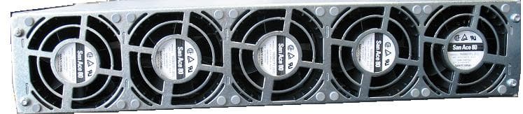
IHET5GX1
Oct 14, 2007UBS CDMA XMI Transceiver at 800 MHz
Equipment Class
TNB - Licensed Non-Broadcast Station Transmitter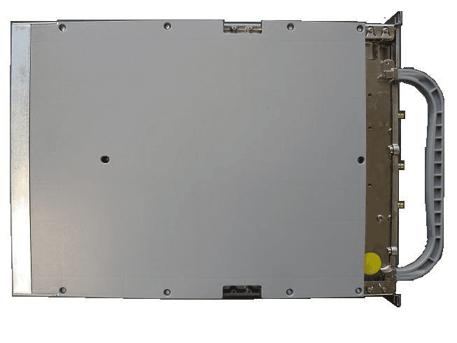
IHET6HG1
Sep 12, 2007CDMA Base Station
Equipment Class
PCB - PCS Licensed Transmitter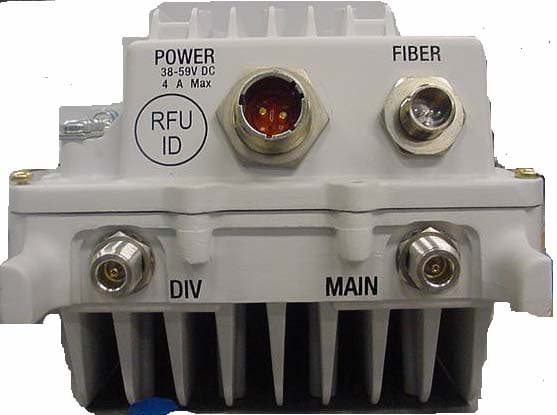
IHET7HN1
Jul 17, 20072.5 GHz Diversity Access Point
Equipment Class
TNB - Licensed Non-Broadcast Station Transmitter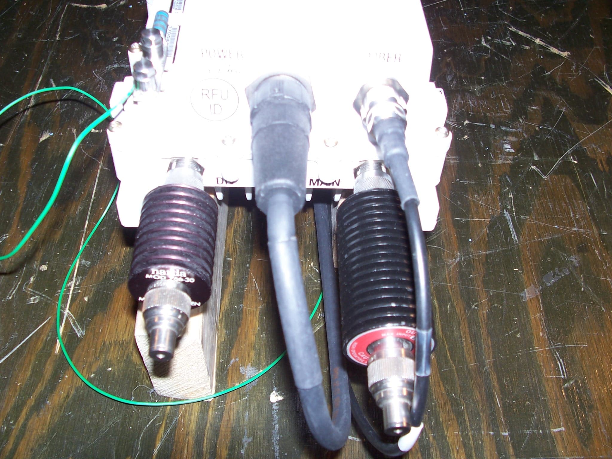
IHET7GT1
Jan 14, 20072.5GHz DIVERSITY ACCESS POINT
Equipment Class
TNB - Licensed Non-Broadcast Station Transmitter