IHET5DS1Cellular CDMA base station
Nokia Solutions and Networks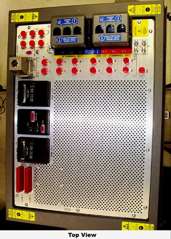
Click to zoom
Application Details
- Equipment Class
- TNB - Licensed Non-Broadcast Station Transmitter
- Date of Grant
- Dec 18, 2003
- Application Purpose
- Original Equipment
- Date of Application
- Dec 18, 2003
- Equipment Note
- Cellular CDMA base station
- Frequency Range
- 869.70000000 - 893.31000000
- Company
- Nokia Solutions and Networks
- Country
- United States
Documents & Files
Document Text
Text extracted from the exhibit documents filed with the FCC. Open a document above to read the original.
Users Manual
1X SCt 4812T BTS Optimization/ATP i Oct 2003 1X SCt 4812T BTS Optimization/ATP Table of Contents . . . Table of Contents 68P09258A31–A 1X SCt 4812T BTS Optimization/ATP ii Oct 2003 Contents FCC Requirementsxviii . . . . . . . . . . . . . . . . . . . . . . . . . . . . . . . . . . . . . . . . . . . . . . . . . . . . . . . . . . . . . . . . . . . . . . . . . . Contentxviii . . . . . . . . . . . . . . . . . . . . . . . . . . . . . . . . . . . . . . . . . . . . . . . . . . . . . . . . . . . . . . . . . . . . . . . . . . . . . FCC Part 15 Requirementsxviii . . . . . . . . . . . . . . . . . . . . . . . . . . . . . . . . . . . . . . . . . . . . . . . . . . . . . . . . . . . . FCC Part 68 Requirementsxix . . . . . . . . . . . . . . . . . . . . . . . . . . . . . . . . . . . . . . . . . . . . . . . . . . . . . . . . . . . . Forewordxx . . . . . . . . . . . . . . . . . . . . . . . . . . . . . . . . . . . . . . . . . . . . . . . . . . . . . . . . . . . . . . . . . . . . . . . . . . . . . . . . . . . General Safetyxxii . . . . . . . . . . . . . . . . . . . . . . . . . . . . . . . . . . . . . . . . . . . . . . . . . . . . . . . . . . . . . . . . . . . . . . . . . . . . . . Revision Historyxxiv . . . . . . . . . . . . . . . . . . . . . . . . . . . . . . . . . . . . . . . . . . . . . . . . . . . . . . . . . . . . . . . . . . . . . . . . . . . . . Chapter 1 Introduction1-1 . . . . . . . . . . . . . . . . . . . . . . . . . . . . . . . . . . . . . . . . . . . . . . . . . . . . Optimization Manual: Scope and Layout1-2 . . . . . . . . . . . . . . . . . . . . . . . . . . . . . . . . . . . . . . . . . . . . . . . . . . . . . . . . Manual Scope and Layout1-2 . . . . . . . . . . . . . . . . . . . . . . . . . . . . . . . . . . . . . . . . . . . . . . . . . . . . . . . . . . . . . Assumptions and Prerequisites1-2 . . . . . . . . . . . . . . . . . . . . . . . . . . . . . . . . . . . . . . . . . . . . . . . . . . . . . . . . Document Composition1-3 . . . . . . . . . . . . . . . . . . . . . . . . . . . . . . . . . . . . . . . . . . . . . . . . . . . . . . . . . . . . . . . Purpose of the Optimization1-4 . . . . . . . . . . . . . . . . . . . . . . . . . . . . . . . . . . . . . . . . . . . . . . . . . . . . . . . . . . . . . . . . . . Why Optimize?1-4 . . . . . . . . . . . . . . . . . . . . . . . . . . . . . . . . . . . . . . . . . . . . . . . . . . . . . . . . . . . . . . . . . . . . . . What Is Optimization?1-4 . . . . . . . . . . . . . . . . . . . . . . . . . . . . . . . . . . . . . . . . . . . . . . . . . . . . . . . . . . . . . . . . What Happens During Optimization?1-4 . . . . . . . . . . . . . . . . . . . . . . . . . . . . . . . . . . . . . . . . . . . . . . . . . . . . When to Optimize1-5 . . . . . . . . . . . . . . . . . . . . . . . . . . . . . . . . . . . . . . . . . . . . . . . . . . . . . . . . . . . . . . . . . . . . . . . . . . . New Installations1-5 . . . . . . . . . . . . . . . . . . . . . . . . . . . . . . . . . . . . . . . . . . . . . . . . . . . . . . . . . . . . . . . . . . . . . Site Expansion1-5 . . . . . . . . . . . . . . . . . . . . . . . . . . . . . . . . . . . . . . . . . . . . . . . . . . . . . . . . . . . . . . . . . . . . . . . Periodic Optimization1-5 . . . . . . . . . . . . . . . . . . . . . . . . . . . . . . . . . . . . . . . . . . . . . . . . . . . . . . . . . . . . . . . . . Repaired Sites1-5 . . . . . . . . . . . . . . . . . . . . . . . . . . . . . . . . . . . . . . . . . . . . . . . . . . . . . . . . . . . . . . . . . . . . . . . Required Test Equipment and Software1-6 . . . . . . . . . . . . . . . . . . . . . . . . . . . . . . . . . . . . . . . . . . . . . . . . . . . . . . . . Overview1-6 . . . . . . . . . . . . . . . . . . . . . . . . . . . . . . . . . . . . . . . . . . . . . . . . . . . . . . . . . . . . . . . . . . . . . . . . . . . . Policy1-6 . . . . . . . . . . . . . . . . . . . . . . . . . . . . . . . . . . . . . . . . . . . . . . . . . . . . . . . . . . . . . . . . . . . . . . . . . . . . . . . Test Equipment Calibration1-6 . . . . . . . . . . . . . . . . . . . . . . . . . . . . . . . . . . . . . . . . . . . . . . . . . . . . . . . . . . . . Test Cable Calibration1-6 . . . . . . . . . . . . . . . . . . . . . . . . . . . . . . . . . . . . . . . . . . . . . . . . . . . . . . . . . . . . . . . . Equipment Warm–up1-7 . . . . . . . . . . . . . . . . . . . . . . . . . . . . . . . . . . . . . . . . . . . . . . . . . . . . . . . . . . . . . . . . . LMF computer and software1-7 . . . . . . . . . . . . . . . . . . . . . . . . . . . . . . . . . . . . . . . . . . . . . . . . . . . . . . . . . . . Communications system analyzer CDMA/analog1-9 . . . . . . . . . . . . . . . . . . . . . . . . . . . . . . . . . . . . . . . . . Optional Equipment1-11 . . . . . . . . . . . . . . . . . . . . . . . . . . . . . . . . . . . . . . . . . . . . . . . . . . . . . . . . . . . . . . . . . . Required Documentation1-12 . . . . . . . . . . . . . . . . . . . . . . . . . . . . . . . . . . . . . . . . . . . . . . . . . . . . . . . . . . . . . . . . . . . . . Required Documents1-12 . . . . . . . . . . . . . . . . . . . . . . . . . . . . . . . . . . . . . . . . . . . . . . . . . . . . . . . . . . . . . . . . . Related Publications1-12 . . . . . . . . . . . . . . . . . . . . . . . . . . . . . . . . . . . . . . . . . . . . . . . . . . . . . . . . . . . . . . . . . . Terms and Abbreviations1-13 . . . . . . . . . . . . . . . . . . . . . . . . . . . . . . . . . . . . . . . . . . . . . . . . . . . . . . . . . . . . . . . . . . . . . Standard and Non–standard Terms and Abbreviations1-13 . . . . . . . . . . . . . . . . . . . . . . . . . . . . . . . . . . . . . BTS Equipment Identification1-15 . . . . . . . . . . . . . . . . . . . . . . . . . . . . . . . . . . . . . . . . . . . . . . . . . . . . . . . . . . . . . . . . . Equipment Overview1-15 . . . . . . . . . . . . . . . . . . . . . . . . . . . . . . . . . . . . . . . . . . . . . . . . . . . . . . . . . . . . . . . . . . Ancillary Equipment Frame Identification1-15 . …
Text truncated - open the document above for the full version.
Users Manual
Preparing the LMF 68P09258A31–A Oct 2003 1X SCt 4812T BTS Optimization/ATP 3-10 LMF Operating System Installation This section provides information and instructions for installing and updating the LMF software and files. NOTE First Time Installation Sequence: 1. Install Java Runtime Environment (JRE) 2. Install U/WIN K–shell emulator 3. Install LMF application programs 4. Install/create BTS folders NOTE Any time you install U/WIN, you must install the LMF software because the installation of the LMF modifies some of the files that are installed during the U/Win installation. Installing U/Win over–writes these modifications. There are multiple binary image packages for installation on the CD–ROM. When prompted, choose the load that corresponds to the switch release that you currently have installed. Perform the Device Images install after the WinLMF installation. If applicable, a separate CD ROM of BTS Binaries may be available for binary updates. Follow the procedure in Table 3-1 to install the LMF application program using the LMF CD ROM. Table 3-1: Install LMF using CD ROM nStepAction 1Insert the LMF CD ROM disk into your disk drive and perform the following as required: 1a– If the Setup screen appears, follow the instructions displayed on the screen. 1b– If the Setup screen is not displayed, proceed to Step 2. 2Click on the Start button. 3Select Run. 4Enter d:\autorun in the Open box and click OK. NOTE If applicable, replace the letter d with the correct CD ROM drive letter. 3 Preparing the LMF68P09258A31–A Oct 2003 1X SCt 4812T BTS Optimization/ATP 3-11 Copy BTS and CBSC CDF (or NECF) Files to the LMF Computer Before logging on to a BTS with the LMF computer to execute optimization/ATP procedures, the correct bts-#.cdf (or bts–#.necf) and cbsc-#.cdf files must be obtained from the CBSC and put in a bts-# folder in the LMF computer. This requires creating versions of the CBSC CDF files on a DOS–formatted floppy diskette and using the diskette to install the CDF files on the LMF computer. NOTE – If the LMF has ftp capability, the ftp method can be used to copy the CDF or NECF files from the CBSC. – On Sun OS workstations, the unix2dos command can be used in place of the cp command (e.g., unix2dos bts–248.cdf bts–248.cdf). This should be done using a copy of the CBSC CDF file so the original CBSC CDF file is not changed to DOS format. NOTE When copying CDF or NECF files, comply with the following to prevent BTS login problems with the Windows LMF: SThe numbers used in the bts-#.cdf (or bts–#.necf) and cbsc-#.cdf filenames must correspond to the locally-assigned numbers for each BTS and its controlling CBSC. SThe generic cbsc–1.cdf file supplied with the Windows LMF will work with locally numbered BTS CDF files. Using this file will not provide a valid optimization unless the generic file is edited to replace default parameters (e.g., channel numbers) with the operational parameters used locally. The procedure in Table 3-2 lists the steps required to transfer the CDF files from the CBSC to the LMF computer. For further information, refer to the LMF Help function on–line documentation. Table 3-2: Copying CDF or NECF Files to the LMF Computer nStepAction AT THE CBSC: 1Login to the CBSC workstation. 2Insert a DOS–formatted floppy diskette in the workstation drive. 3Type eject –q and press the Enter key. 4Type mount and press the Enter key. NOTE SLook for the “floppy/no_name” message on the last line displayed. SIf the eject command was previously entered, floppy/no_name will be appended with a number. Use the explicit floppy/no_name reference displayed when performing Step 7. 5Change to the directory, where the files to be copied reside, by typing cd <directoryname> (e.g., cd bts–248) and pressing the Enter key. 6Type ls and press the Enter key to display the list of files in the directory. . . . continued on next page 3 Preparing the LMF 68P09258A31–A Oct 2003 1X SCt 4812T BTS Optimization/ATP 3-12 Table 3-2: Copying CDF or NECF Files to the LMF Computer nActionStep 7With Solaris versions of Unix, create DOS–formatted versions of the bts-#.cdf (or bts–#.necf) and cbsc-#.cdf files on the diskette by entering the following command: unix2dos <source filename> /floppy/no_name/<target filename> (e.g., unix2dos bts–248.cdf /floppy/no_name/bts–248.cdf). NOTE SOther versions of Unix do not support the unix2dos and dos2unix commands. In these cases, use the Unix cp (copy) command. The copied files will be difficult to read with a DOS or Windows text editor because Unix files do not contain line feed characters. Editing copied CDF files on the LMF computer is, therefore, not recommended. SUsing cp, multiple files can be copied in one operation by separating each filename to be copied with a space and ensuring the destination directory (floppy/no_name) is listed at the end of the command string following a space (e.g., cp bts–248.cdf cbsc–6.cdf /floppy/no_name). 8Repeat Steps 5 through 7 for each bts–# that must be supported by the LMF computer. 9When all required files have been copied to the diskette type eject and press the Enter key. 10Remove the diskette from the CBSC drive. AT THE LMF: 11If it is not running, start the Windows operating system on the LMF computer. 12Insert the diskette containing the bts-#.cdf (or bts–#.necf) and cbsc-#.cdf files into the LMF computer. 13Using MS Windows Explorer, create a corresponding bts–# folder in the <x>:\<lmf home directory>\cdma directory for each bts-#.cdf (or bts–#.necf) and cbsc-#.cdf file pair copied from the CBSC. 14Use MS Windows Explorer to transfer the bts-#.cdf (or bts–#.necf) and cbsc-#.cdf files from the diskette to the corresponding <x>:\<lmf home directory>\cdma\bts–# folders created in Step 13. 3 Preparing the LMF68P09258A31–A Oct 2003 1X SCt 4812T BTS Optimization/ATP 3-13 Creating a Named HyperTerminal Connection for MMI Connection Confirming or changing the configuration data of certain BTS Field Replaceable Units (FRU) requires establi…
Text truncated - open the document above for the full version.
Users Manual
Bay Level Offset Calibration68P09258A31–A Oct 2003 1X SCt 4812T BTS Optimization/ATP 3-89 Test Equipment Set-up for RF Path Calibration Follow the procedure in Table 3-35 to set up test equipment. Table 3-35: Set Up Test Equipment for RF Path Calibration StepAction 1If it has not already been done, refer to the procedure in Table 3-5 (on page 3-17) to interface the LMF computer terminal to the frame LAN A connector. 2If it has not already been done, refer to Table 3-6 (on page 3-26) to start a GUI LMF session. 3If required, calibrate the test equipment per the procedure in Table 3-27 (on page 3-78). NOTE Verify the GPIB controller is properly connected and turned on. ! CAUTION To prevent damage to the test equipment, all transmit (TX) test connections must be via the 30 dB directional coupler for 800 MHz with an additional 20 dB in–line attenuator for 1.7/1.9 GHz. 4For TX path calibration, connect the test equipment as shown in Figure 3-16, Figure 3-17, or Figure 3-19, depending on the communications analyzer being used. Transmit (TX) Path Calibration Description The assigned channel frequency and power level (as measured at the top of the frame) for transmit calibration are derived from the site CDF files. For each BBX, the channel frequency is specified in the ChannelList CDF file parameter and the power is specified in the SIFPilotPwr CDF file parameter for the sector associated with the BBX (located under the ParentSECTOR field of the ParentCARRIER CDF file parameter). NOTE If both the BTS–x.cdf and CBSC–x.cdf files are current, all information will be correct on the LMF. If not, the carrier and channel will have to be set for each test. The calibration procedure attempts to adjust the power to within +0.5 dB of the desired power. The calibration will pass if the error is less than + 1.5 dB. The TX Bay Level Offset at sites WITHOUT the directional coupler option, is approximately 42.0 dB ±3.0 dB. SAt sites WITHOUT RFDS option, BLO is approximately 42.0 dB ±4.0 dB. A typical example would be TX output power measured at BTS (36.0 dBm) minus the BBX TX output level (approximately –6.0 dBm) would equate to 42 dB BLO. The TX Bay Level Offset at sites WITH the directional coupler option, is approximately 41.4 dB ±3.0 dB. TX BLO = Frame Power Output minus BBX output level. SExample: TX output power measured at RFDS TX coupler (39.4 dBm) minus the BBX TX output level (approximately –2.0 dBm) and RFDS directional coupler/cable (approximately –0.6 dBm) would equate to 41.4 dB BLO. 3 Bay Level Offset Calibration 68P09258A31–A Oct 2003 1X SCt 4812T BTS Optimization/ATP 3-90 TX Calibration and the LMF The LMF Tests > TX > TX Calibration... and Tests > All Cal/Audit... selections perform TX BLO calibration testing for installed BBX(s). The All Cal/Audit... selection initiates a series of actions to perform TX calibration, and if calibration is successful, download BLO and perform TX audit. The TX Calibration... selection performs only TX calibration. When TX Calibration... is used, BLO download and TX audit must be performed as separate activities. The CDMA Test Parameters window which opens when TX Calibration... or All Cal/Audit... is selected contains several user–selectable features which are described in the following subsections. Rate Set Drop-down Pick List The Rate Set Drop–down Box is enabled if at least one MCC card is selected for the test. The available options for TX tests are 1 = 9600, and 3 = 9600 1X. Option 3 is only available if 1X cards are selected for the test. The available transfer rate options for RX tests are 1 = 9600 and 2 = 14400. Option 2 is only available if no 1X cards are selected. Verify BLO In both the TX Calibration and All Cal/Audit dialog boxes, a Verify BLO checkbox is provided and checked by default. After the actual TX calibration is completed during either the TX Calibration or All Cal/Audit process, the BLO derived from the calibration is compared to a standard, acceptable BLO tolerance for the BTS. In some installations, additional items may be installed in the transmit path. The additional change in gain from these items could cause BLO verification failure and, therefore, failure of the entire calibration. In these cases, either the Verify BLO checkbox should be unchecked or the additional path losses should be added into each applicable sector using the Util>Edit>TX Coupler Loss... function. Single-Sided BLO Checkbox Another option that appears in the pull–down menu is Single–sided BLO. Normally valid BLO values are some value plus–or–minus some offset. The ranges that we currently use for calibration are wider than necessary to accommodate the redundant BBX. The lower half of that range is where non–redundant BBXs should be. When Single–sided BLO is selected, the result is only considered a success if it is in the lower half of the range. If it was normally a success from 37–47 (which is 42 "5), Single–sided BLO would make it a success only if the result was from 37–42. To get the more stringent conditions, the operator checks Single–sided BLO when calibrating non–redundant transceivers. Single–sided BLO carries the likelihood of more failures. This option should only be used by experienced CFEs. 3 Bay Level Offset Calibration68P09258A31–A Oct 2003 1X SCt 4812T BTS Optimization/ATP 3-91 Test Pattern Drop-down Pick List The Tests > TX > TX Calibration... menu window has a Test Pattern pull–down menu. This menu has the following choices: SPilot (default) – performs tests using a pilot signal only. This pattern should be used when running in–service tests. It only requires a BBX to do the test. SStandard – performs the tests using pilot, synch, paging and six traffic channels. This pattern should be used on all non–in–service tests. Standard requires a BBX and an MCC. Standard uses gain values specified by the IS97 standard. SCDFPilot –performs the tests using the pilot signal, however, the gain is specified in the CDF file. Advanced users may use CDFPilot…
Text truncated - open the document above for the full version.
Attestation Statements
M APPLICANT: MOTOROLA Global Telecom Solutions Sector FCC ID: IHET5DS1 FCC Filing – SC4812T 1X / 1X-EVDO @ 800 MHz CDMA BTS 1 of 3 STATEMENTS OF CERTIFICATION EXHIBIT M APPLICANT: MOTOROLA Global Telecom Solutions Sector FCC ID: IHET5DS1 FCC Filing – SC4812T 1X / 1X-EVDO @ 800 MHz CDMA BTS 2 of 3 STATEMENT OF CERTIFICATION The technical data supplied with this application, having been taken under our supervision is hereby duly certified. We also certify that this transmit and receive equipment (transceiver type: IHET5DS1) for cellular system use is in full compliance with all parts of EIA/TIA/IS 97-D “Recommended Minimum Performance Standards for Base Stations Supporting Dual Mode Wideband Spread Spectrum Cellular Mobile Stations,” and the applicable portions of FCC Part 22 Name: Terry Schwenk Position: Engineering Section Manager Customer Integration Engineering Signed: Date: 10/20/2003 I hereby certify that the above application was prepared under my direction and that to the best of my knowledge and belief, the facts set forth in this application and accompanying technical data are true and correct. Name: Scott Munier Position: Senior Resource Manager Customer Integration Engineering M APPLICANT: MOTOROLA Global Telecom Solutions Sector FCC ID: IHET5DS1 FCC Filing – SC4812T 1X / 1X-EVDO @ 800 MHz CDMA BTS 3 of 3 ATTESTATION OF COMPLIANCE TESTING The transceiver type IHET5DS1 has been tested in accordance with the requirement contained in the appropriate Commission’s regulations. To the best of my knowledge, these tests were performed using measurement procedures consistent with industry or Commission standards and demonstrate that this equipment complies with the appropriate standards. Each unit manufactured, imported or marketed, will conform to the sample tested within the variations that can be expected due to quantity production and testing on a statistical basis. I further certify that the necessary measurements were made at Motorola Inc., located at 1475 W. Shure Dr., Arlington Heights, IL 60004, or at the UL International EMC Lab radiation test facility located at 333 Pfingsten Road, Northbrook, IL 60062-2096 Name: Scott Munier Position: Senior Resource Manager Customer Integration Engineering
Block Diagram
12 12 12RX Main 12 TX 12RX Div High Power LPAs + Trunking Modules MCC1X HP BBX1X (Redundant) HP Switch Power Supply CDMA Clock Distribution Clock Synch Module MPC3 Span IO High Stability Oscillator C-CCP Shelf GLI2 AMR GPS RX Filters 6 or 12 6 or 12 6 or 12 Clk/Sync 2 12 12 Filter / Combiner Filter / Combiner if 3 sector 3 TCH Data13 Fwd13 Rvs CT1 SpanTo/From CBSC 3 6 RX TX Optional Comm / Bus Clk / Sync RF 2 2 Customer Alarms Site IO LAN In / Out To LMF HP BBX1X CIO Rx Rx Tx Tx Remote GPS Dist Optional -48V SC4812T @ 800 MHz CDMA BTS Frame Block Diagram
Cover Letter(s)
M APPLICANT: MOTOROLA Global Telecom Solutions Sector FCC ID: IHET5DS1 FCC Filing – SC4812T 1X / 1X-EVDO @ 800 MHz CDMA BTS 1 of 2 October 16, 2003 Federal Communications Commission Authorization & Evaluation Division 7435 Oakland Mills Road Columbia, Maryland 21046 Re: Application for Cellular Transceiver Certification Gentlemen: Motorola Inc., 1475 W. Shure Drive, Arlington Heights, Illinois 60004, herein submits: Filing fee, Application for Equipment Authorization (FCC Form 731) and Sections, for Certification of a Cellular Transceiver, FCC ID: IHET5DS1. Motorola is also the manufacturer of this equipment. Motorola requests that the following Sections of the Schematics Exhibit be kept confidential: Section A MPC6 - Multicoupler Preselector Card Section B GLI2 - Group Line Interface Card Section C GLI3 - Group Line Interface Card Section D BBX2 - Broadband Transceiver Card Section E BBX-1X – Broadband Transceiver Card Section F BBX-1X-HP – Broadband Transceiver Card Section G MCC x 24E - Multi Channel CDMA Card Section H MCC-1X – Multi Channel CDMA Card Section I MCC-DO – Multi Channel CDMA Card Section J CCD - CDMA Clock Distribution Card Section K CSM2 - Clock Synchronization Module w/GPS Section L LPA - Linear Power Amplifier Section M CIO - Combiner Input/Output Card Section N Switch Card Section O HSO - High Stability Oscillator Section P SPAN I/O Section Q RGD - Remote GPS Distribution Section R LFR – Low Frequency Receiver Special Note The confidential portions have been identified as such on the Uploading Sections Form. The filing fee includes $145.00, the amount for a confidential filing. M APPLICANT: MOTOROLA Global Telecom Solutions Sector FCC ID: IHET5DS1 FCC Filing – SC4812T 1X / 1X-EVDO @ 800 MHz CDMA BTS 2 of 2 This equipment has the capability to operate using Code Division Multiple Access (CDMA) on a spread spectrum signal operating in the cellular band. This more efficient modulation scheme can provide 3 to 10 times the number of available voice channels when compared to existing analog technologies. Technical details for this alternate cellular technology (permitted under the cellular service option provisions in section 24 of the Commission’s rules) related to certification of this equipment, are provided in the Statements of Certification Exhibit, and throughout the other exhibits. Please contact me by telephone at (847) 435-9487, by Fax at (847) 632-5936, or by correspondence at the address herein if there are further questions or if additional information is needed concerning this filing. Regards, Scott Munier Senior Resource Manager Customer Integration Engineering
External Photos
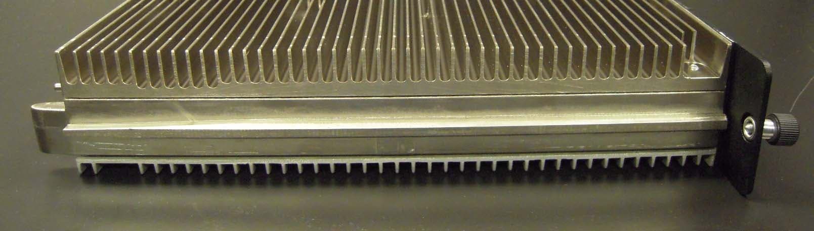
M APPLICANT: MOTOROLA Global Telecom Solutions Sector FCC ID: IHET5DS1 FCC Filing – SC4812T 1X / 1X-EVDO @ 800 MHz CDMA BTS 1 of 8 External Photos Exhibit SC4812T 1X / 1X-EVDO @ 800 MHz CDMA BTS Number Description 1 Front View Doors Closed 2 Front View Doors Open 3 Rear View with Panel 4 Rear View without Panel 5 Left Side View 6 Right Side View 7 Top View
ID Label/Location Info
EQUIPMENT NAMEPLATE PER CFR., Title 47, Part 2.925 Bar Coding Graphics to be black A name plate of this type, or one similar to it, will be affixed to every base station. This label is permanent, indelible, and tamper evident. || | |||| | ||| | |||||| | | ||||| ||| ||| || | | |||||| Serial No. Complies with Part 68, FCC Rules Model No. _____________ ||||| | | ||| |||| ||||| | | | ||||| | |||| ||| || || || | | FCC Reg. No. REN: USOC: MOTOROLA FCC ID: C S M 2 C S M 1 IF M/ DI S A M L F R/ H A M R/ M AC H B A M R/ M AC H B Cl oc k Cl oc k GL I2 B GL I2 A M CC 24 - 7 M CC 24 - 8 M CC 24 - 9 M CC 24 - 10 M CC 24 - 11 M CC 24 - 12 M CC 24 - 1 M CC 24 - 2 M CC 24 - 3 M CC 24 - 4 M CC 24 - 5 M CC 24 - 6 BB X 1 BB X 2 BB X 3 BB X 4 BB X 5 BB X 6 BB X Re du nd ant BB X 7 BB X 8 BB X 9 BB X 10 BB X 11 BB X 12 BB X Ma trix CI O M P C B M P C A B Po we r Su pp ly 2 C Po we r Su pp ly 3 A Po we r Su pp ly 1 19 m m Fill er Pa nel MOTOROLA PS2 PS3 1A 1B PS1 1C 1D 2A 2B 2C 2D 3A 3B 3C 3D 4A 4B 4C 4D L P A LPA MAPPING C C P LAN Access Panel SC4812T 1X / 1X-EVDO CDMA BTS Frame Label Location ID Label Location
Internal Photos
M Internal Photos Exhibit Global Telecom Solutions Sector FCC ID: IHET5DS1 FCC Filing – SC4812T 1X / 1X-EVDO @ 800 MHz CDMA BTS Page 1 of 43 Internal Photos Exhibit MPC – Front View M Internal Photos Exhibit Global Telecom Solutions Sector FCC ID: IHET5DS1 FCC Filing – SC4812T 1X / 1X-EVDO @ 800 MHz CDMA BTS Page 2 of 43 Internal Photos Exhibit MPC - Rear View M Internal Photos Exhibit Global Telecom Solutions Sector FCC ID: IHET5DS1 FCC Filing – SC4812T 1X / 1X-EVDO @ 800 MHz CDMA BTS Page 3 of 43 Internal Photos Exhibit Group Line Interface II (GLI2) - Front View M Internal Photos Exhibit Global Telecom Solutions Sector FCC ID: IHET5DS1 FCC Filing – SC4812T 1X / 1X-EVDO @ 800 MHz CDMA BTS Page 4 of 43 Internal Photos Exhibit Group Line Interface II (GLI2) - Rear View M Internal Photos Exhibit Global Telecom Solutions Sector FCC ID: IHET5DS1 FCC Filing – SC4812T 1X / 1X-EVDO @ 800 MHz CDMA BTS Page 5 of 43 Internal Photos Exhibit Group Line Interface (GLI3) - Front View M Internal Photos Exhibit Global Telecom Solutions Sector FCC ID: IHET5DS1 FCC Filing – SC4812T 1X / 1X-EVDO @ 800 MHz CDMA BTS Page 6 of 43 Internal Photos Exhibit Group Line Interface (GLI3) - Rear View M Internal Photos Exhibit Global Telecom Solutions Sector FCC ID: IHET5DS1 FCC Filing – SC4812T 1X / 1X-EVDO @ 800 MHz CDMA BTS Page 7 of 43 Internal Photos Exhibit BBX2 – Front View M Internal Photos Exhibit Global Telecom Solutions Sector FCC ID: IHET5DS1 FCC Filing – SC4812T 1X / 1X-EVDO @ 800 MHz CDMA BTS Page 8 of 43 Internal Photos Exhibit BBX2 – Rear View M Internal Photos Exhibit Global Telecom Solutions Sector FCC ID: IHET5DS1 FCC Filing – SC4812T 1X / 1X-EVDO @ 800 MHz CDMA BTS Page 9 of 43 Internal Photos Exhibit BBX-1X - Front View M Internal Photos Exhibit Global Telecom Solutions Sector FCC ID: IHET5DS1 FCC Filing – SC4812T 1X / 1X-EVDO @ 800 MHz CDMA BTS Page 10 of 43 Internal Photos Exhibit BBX-1X - Rear View M Internal Photos Exhibit Global Telecom Solutions Sector FCC ID: IHET5DS1 FCC Filing – SC4812T 1X / 1X-EVDO @ 800 MHz CDMA BTS Page 11 of 43 Internal Photos Exhibit BBX-1X HP - Front View M Internal Photos Exhibit Global Telecom Solutions Sector FCC ID: IHET5DS1 FCC Filing – SC4812T 1X / 1X-EVDO @ 800 MHz CDMA BTS Page 12 of 43 Internal Photos Exhibit BBX-1X HP - Rear View M Internal Photos Exhibit Global Telecom Solutions Sector FCC ID: IHET5DS1 FCC Filing – SC4812T 1X / 1X-EVDO @ 800 MHz CDMA BTS Page 13 of 43 Internal Photos Exhibit MCCx24E - Front View M Internal Photos Exhibit Global Telecom Solutions Sector FCC ID: IHET5DS1 FCC Filing – SC4812T 1X / 1X-EVDO @ 800 MHz CDMA BTS Page 14 of 43 Internal Photos Exhibit MCCx24E - Rear View M Internal Photos Exhibit Global Telecom Solutions Sector FCC ID: IHET5DS1 FCC Filing – SC4812T 1X / 1X-EVDO @ 800 MHz CDMA BTS Page 15 of 43 Internal Photos Exhibit MCC-1X - Front View M Internal Photos Exhibit Global Telecom Solutions Sector FCC ID: IHET5DS1 FCC Filing – SC4812T 1X / 1X-EVDO @ 800 MHz CDMA BTS Page 16 of 43 Internal Photos Exhibit MCC-1X - Rear View M Internal Photos Exhibit Global Telecom Solutions Sector FCC ID: IHET5DS1 FCC Filing – SC4812T 1X / 1X-EVDO @ 800 MHz CDMA BTS Page 17 of 43 Internal Photos Exhibit MCC-DO - Front View M Internal Photos Exhibit Global Telecom Solutions Sector FCC ID: IHET5DS1 FCC Filing – SC4812T 1X / 1X-EVDO @ 800 MHz CDMA BTS Page 18 of 43 Internal Photos Exhibit MCC-DO - Rear View M Internal Photos Exhibit Global Telecom Solutions Sector FCC ID: IHET5DS1 FCC Filing – SC4812T 1X / 1X-EVDO @ 800 MHz CDMA BTS Page 19 of 43 Internal Photos Exhibit CCD - Front View M Internal Photos Exhibit Global Telecom Solutions Sector FCC ID: IHET5DS1 FCC Filing – SC4812T 1X / 1X-EVDO @ 800 MHz CDMA BTS Page 20 of 43 Internal Photos Exhibit CCD - Rear View M Internal Photos Exhibit Global Telecom Solutions Sector FCC ID: IHET5DS1 FCC Filing – SC4812T 1X / 1X-EVDO @ 800 MHz CDMA BTS Page 21 of 43 Internal Photos Exhibit CSM2 - Front View M Internal Photos Exhibit Global Telecom Solutions Sector FCC ID: IHET5DS1 FCC Filing – SC4812T 1X / 1X-EVDO @ 800 MHz CDMA BTS Page 22 of 43 Internal Photos Exhibit CSM2 - Rear View M Internal Photos Exhibit Global Telecom Solutions Sector FCC ID: IHET5DS1 FCC Filing – SC4812T 1X / 1X-EVDO @ 800 MHz CDMA BTS Page 23 of 43 Internal Photos Exhibit LPA – Front View M Internal Photos Exhibit Global Telecom Solutions Sector FCC ID: IHET5DS1 FCC Filing – SC4812T 1X / 1X-EVDO @ 800 MHz CDMA BTS Page 24 of 43 Internal Photos Exhibit LPA - Rear View M Internal Photos Exhibit Global Telecom Solutions Sector FCC ID: IHET5DS1 FCC Filing – SC4812T 1X / 1X-EVDO @ 800 MHz CDMA BTS Page 25 of 43 Internal Photos Exhibit LPA - Front View (no cover) M Internal Photos Exhibit Global Telecom Solutions Sector FCC ID: IHET5DS1 FCC Filing – SC4812T 1X / 1X-EVDO @ 800 MHz CDMA BTS Page 26 of 43 Internal Photos Exhibit Power Supply - Front View M Internal Photos Exhibit Global Telecom Solutions Sector FCC ID: IHET5DS1 FCC Filing – SC4812T 1X / 1X-EVDO @ 800 MHz CDMA BTS Page 27 of 43 Internal Photos Exhibit Power Supply - Rear View M I…
Text truncated - open the document above for the full version.
Contact Information
Applicant
Steve Mitchell
Technical Contact
Motorola IncTerry Schwenk
[email protected]847-435-0780
1475 W. Shure Drive, IL75, Room 4000B · Arlington Heights, Illinois · United States
Non-Technical Contact
Motorola IncFransisco Avalos
[email protected]847-435-9743
Test Firm
UL LLCRick Titus
Technical Specifications
| # | Rule Parts | Frequency Range | Power Output | Emission | Tolerance |
|---|---|---|---|---|---|
| 2 | 22H | 869.7 MHz - 893.31 MHz | 60 W | 1M30F9W | 1.5 ppm |
Other Applications from Nokia Solutions and Networks
IHET4KJ1
Apr 28, 2010LTE 700 MHz Public Safety Base Station Transceiver
Equipment Class
TNB - Licensed Non-Broadcast Station Transmitter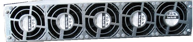
IHET5GX1
Oct 14, 2007UBS CDMA XMI Transceiver at 800 MHz
Equipment Class
TNB - Licensed Non-Broadcast Station Transmitter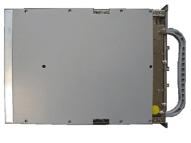
IHET6HG1
Sep 12, 2007CDMA Base Station
Equipment Class
PCB - PCS Licensed Transmitter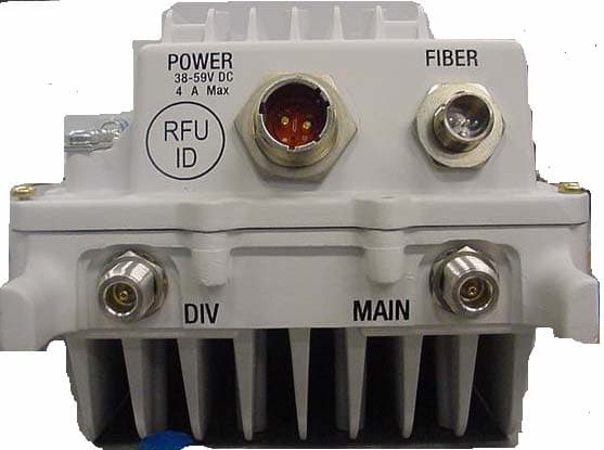
IHET7HN1
Jul 17, 20072.5 GHz Diversity Access Point
Equipment Class
TNB - Licensed Non-Broadcast Station Transmitter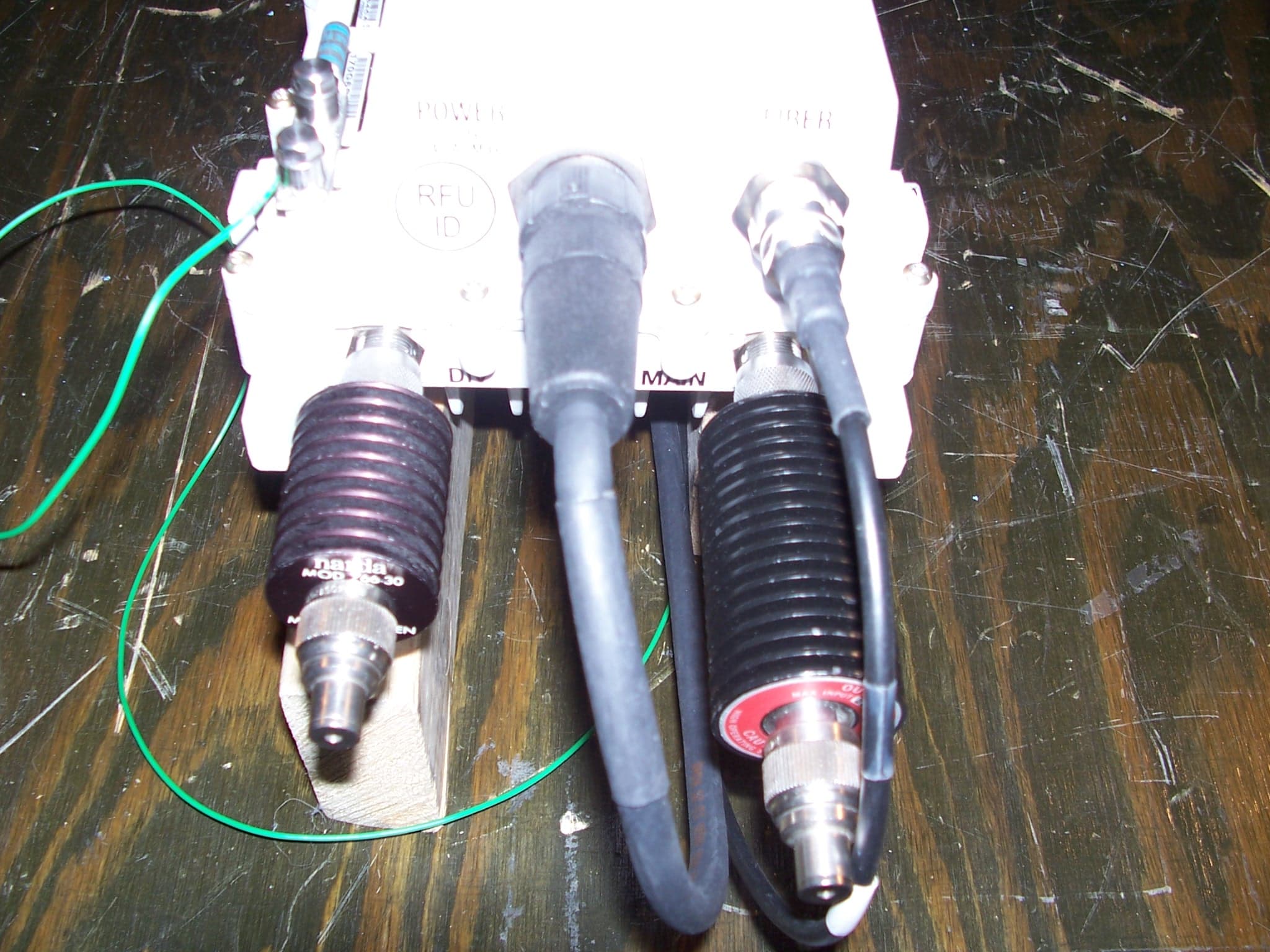
IHET7GT1
Jan 14, 20072.5GHz DIVERSITY ACCESS POINT
Equipment Class
TNB - Licensed Non-Broadcast Station Transmitter