IHET5EJ11X SC480 BTS Microcell Base Station Transmitter
Nokia Solutions and Networks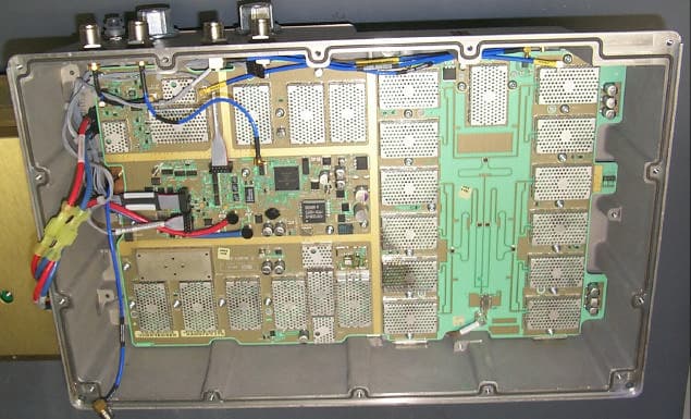
Click to zoom
Application Details
- Equipment Class
- TNB - Licensed Non-Broadcast Station Transmitter
- Date of Grant
- Jun 10, 2004
- Application Purpose
- Original Equipment
- Date of Application
- Jun 10, 2004
- Equipment Note
- 1X SC480 BTS Microcell Base Station Transmitter
- Frequency Range
- 869.70000000 - 893.31000000
- Company
- Nokia Solutions and Networks
- Country
- United States
Documents & Files
Document Text
Text extracted from the exhibit documents filed with the FCC. Open a document above to read the original.
Users Manual
PRELIMINARY 68P09260A11–7 MAY 2004 ENGLISH CDMA2000 1X SOFTWARE RELEASE 2.16.4.X Technical Information 1X SC480 BTS HARDWARE INSTALLATION, OPTIMIZATION/ATP, AND FRU 800 MHZ PRELIMINARY SPECIFICATIONS SUBJECT TO CHANGE WITHOUT NOTICE Notice While reasonable efforts have been made to assure the accuracy of this document, Motorola, Inc. assumes no liability resulting from any inaccuracies or omissions in this document, or from use of the information obtained herein. The information in this document has been carefully checked and is believed to be entirely reliable. However, no responsibility is assumed for inaccuracies or omissions. Motorola, Inc. reserves the right to make changes to any products described herein and reserves the right to revise this document and to make changes from time to time in content hereof with no obligation to notify any person of revisions or changes. Motorola, Inc. does not assume any liability arising out of the application or use of any product, software, or circuit described herein; neither does it convey license under its patent rights or the rights of others. It is possible that this publication may contain references to, or information about Motorola products (machines and programs), programming, or services that are not announced in your country. Such references or information must not be construed to mean that Motorola intends to announce such Motorola products, programming, or services in your country. Copyrights This instruction manual, and the Motorola products described in this instruction manual may be, include or describe copyrighted Motorola material, such as computer programs stored in semiconductor memories or other media. Laws in the United States and other countries preserve for Motorola and its licensors certain exclusive rights for copyrighted material, including the exclusive right to copy, reproduce in any form, distribute and make derivative works of the copyrighted material. Accordingly, any copyrighted material of Motorola and its licensors contained herein or in the Motorola products described in this instruction manual may not be copied, reproduced, distributed, merged or modified in any manner without the express written permission of Motorola. Furthermore, the purchase of Motorola products shall not be deemed to grant either directly or by implication, estoppel, or otherwise, any license under the copyrights, patents or patent applications of Motorola, as arises by operation of law in the sale of a product. Usage and Disclosure Restrictions License Agreement The software described in this document is the property of Motorola, Inc and its licensors. It is furnished by express license agreement only and may be used only in accordance with the terms of such an agreement. Copyrighted Materials Software and documentation are copyrighted materials. Making unauthorized copies is prohibited by law. No part of the software or documentation may be reproduced, transmitted, transcribed, stored in a retrieval system, or translated into any language or computer language, in any form or by any means, without prior written permission of Motorola, Inc. High Risk Activities Components, units, or third–party products used in the product described herein are NOT fault–tolerant and are NOT designed, manufactured, or intended for use as on–line control equipment in the following hazardous environments requiring fail–safe controls: the operation of Nuclear Facilities, Aircraft Navigation or Aircraft Communication Systems, Air Traffic Control, Life Support, or Weapons Systems (“High Risk Activities”). Motorola and its supplier(s) specifically disclaim any expressed or implied warranty of fitness for such High Risk Activities. Trademarks MOTOROLA and the Stylized M Logo are registered in the US Patent & Trademark Office. All other product or service names are the property of their respective owners. © Copyright 2003, 2004 Motorola, Inc. Javat Technology and/or J2MEt: Java and all other Java–based marks are trademarks or registered trademarks of Sun Microsystems, Inc. in the U.S. and other countries. UNIX R : UNIX is a registered trademark of The Open Group in the United States and other countries. REV091302 MAY 20041X SC480 BTS Hardware Installation, Optimization/ATP, and FRU i PRELIMINARY Table of Contents 1X SC480 BTS Hardware Installation, Optimization/ATP, and FRU Software Release 2.16.4.X List of Figuresvi . . . . . . . . . . . . . . . . . . . . . . . . . . . . . . . . . . . . . . . . . . . . . . . . . . . List of Tablesxii . . . . . . . . . . . . . . . . . . . . . . . . . . . . . . . . . . . . . . . . . . . . . . . . . . . Forewordxx . . . . . . . . . . . . . . . . . . . . . . . . . . . . . . . . . . . . . . . . . . . . . . . . . . . . . . . FCC Requirementsxxiv . . . . . . . . . . . . . . . . . . . . . . . . . . . . . . . . . . . . . . . . . . . . . . . Contentxxiv . . . . . . . . . . . . . . . . . . . . . . . . . . . . . . . . . . . . . . . . . . . . . . . . . . FCC Part 15 Requirementsxxiv . . . . . . . . . . . . . . . . . . . . . . . . . . . . . . . . . . Part 68 Requirementsxxv . . . . . . . . . . . . . . . . . . . . . . . . . . . . . . . . . . . . . . . General Safetyxxvii . . . . . . . . . . . . . . . . . . . . . . . . . . . . . . . . . . . . . . . . . . . . . . . . . . . Revision Historyxxix . . . . . . . . . . . . . . . . . . . . . . . . . . . . . . . . . . . . . . . . . . . . . . . . . Chapter 1: Introduction Introduction1-1 . . . . . . . . . . . . . . . . . . . . . . . . . . . . . . . . . . . . . . . . . . . . . . . . . . . . . Required Documents1-5 . . . . . . . . . . . . . . . . . . . . . . . . . . . . . . . . . . . . . . . . . . . . . . 800 MHz CDMA Frequencies and Channels1-8 . . . . . . . . . . . . . . . . . . . . . . . . . . . Installation Tools and Materials1-11 . . . . . . . . . . . . . . . . . . . . . . . . . . . . . . . . . . . . . ATP Tools and Materials1-14 . . . . . . . . . . . . . . . . . . . . . . . . . . . . . . . . . . . . …
Text truncated - open the document above for the full version.
Users Manual
Frame Configuration DIP Switch – continued MAY 20041X SC480 BTS Hardware Installation, Optimization/ATP, and FRU 5-3 PRELIMINARY Expansion 1 Frame DIP Switch The switch settings must be verified and set before power is applied to the BTS. Refer to Figure 5-2 or Table 5-2 for the expansion 1 frame. Table 5-2: Frame ID Switch Position – Expansion 1 Frame 1234 DNUP–––– –– = Don’t Care. These switch positions do not affect the BTS. Expansion 2 Frame DIP Switch The switch settings must be verified and set before power is applied to the BTS. Refer to Figure 5-2 or Table 5-3 for Expansion 2 frame. Table 5-3: Frame ID Switch Position – Expansion 2 Frame 1234 UPDN–––– –– = Don’t Care. These switch positions do not affect the BTS. Expansion 3 Frame DIP Switch The switch settings must be verified and set before power is applied to the BTS. Refer to Figure 5-2 or Table 5-4 for Expansion 3 frame. Table 5-4: Frame ID Switch Position – Expansion 3 Frame 1234 DNDN–––– –– = Don’t Care. These switch positions do not affect the BTS. 5 Pre–Power Up Test (Indoor) 5-41X SC480 BTS Hardware Installation, Optimization/ATP, and FRUMAY 2004 PRELIMINARY Objective This procedure check for any electrical problems and verifies the operation and tolerances of the cell site BTS power supply prior to applying power for the first time. Power for EV–DO Information for applying power to a BTS equipped with EV–DO (MCC–DO) can be found in 1xEV–DO Hardware Installation manual – 68P09257A95 Test Equipment The following test equipment is required to perform the Pre–Power Up test: SDigital Multimeter (DMM) Before handling any circuit cards or modules, be sure to wear a grounding strap to prevent damage from ESD. CAUTION Cabling Inspection Using the site specific documentation generated by Motorola Systems Engineering, verify that the following cable systems are properly connected: SDC Power cabling SReceive RF cabling STransmit RF cabling SGPS DC Power Pre–Test Perform the procedure Table 5-5 in before applying any power to the BTS. Table 5-5: BTS DC Pre–Power Test StepAction * IMPORTANT When handling circuit boards and modules, be sure to wear a grounding strap to prevent damages caused by ESD. 1Remove front panel cover. 2Unseat all circuit boards and modules, but do not remove them from their slots. table continued on next page 5 Pre–Power Up Test (Indoor) – continued MAY 20041X SC480 BTS Hardware Installation, Optimization/ATP, and FRU 5-5 PRELIMINARY Table 5-5: BTS DC Pre–Power Test StepAction 3At the rear of the BTS, verify that 20 or 25 A circuit breaker is OFF (pulled out). See Figure 5-3 or Figure 1-9. 4Use a DMM (set to ohms) and verify the resistance on the –48V or +27V bus. – Remove the Power Supply Module from the CCP2 Shelf – Verify that the resistance from the power (+) feed terminal with respect to ground measures > 500 W See Figure 5-3 for –48VDC or Figure 1-9 for +27VDC – Verify that the resistance from the power (–) feed terminal with respect to ground measures > 500 W See Figure 5-3 for –48VDC or Figure 1-9 for +27VDC The resistance measurement should not read 0 (zero). 5Re–seat all circuit boards into their slots 6Install the Power Supply Module into its slot. 7Install front panel cover. GROUND Location (Screw Holes) DC Power Terminal Strip Circuit Breaker Figure 5-3: Location of Circuit Breaker for –48 VDC 20A cCLPA DC Power Pre–Test Perform the procedure Table 5-6 in before applying any power to the cCLPA. 5 Pre–Power Up Test (Indoor) – continued 5-61X SC480 BTS Hardware Installation, Optimization/ATP, and FRUMAY 2004 PRELIMINARY Table 5-6: cCLPA DC Pre–Power Test StepAction 1Ensure that DC power is disengaged at the source. Verify that the DC power cable has been connected using the procedure in Table 4-8. 2Remove I/O panel cover. 3At the bottom of the cCLPA, verify that 20 A circuit breaker to OFF (pulled out). See Figure 5-4. 4Us a DMM (set to ohms) and verify the resistance on the –48V or +27 V bus. – Verify that the resistance from the power (+) feed terminal with respect to ground measures > 500 W – Verify that the resistance from the power (–) feed terminal with respect to ground measures > 500 W The resistance measurement should not read 0 (zero). 5Proceed to Initial Power up procedure in Table 5-11. ti–cdma–wp–00298–v01–ildoc–ah 20A FUSE Figure 5-4: Bottom View of cCLPA 5 AC Power Input (Outdoor Configuration) MAY 20041X SC480 BTS Hardware Installation, Optimization/ATP, and FRU 5-7 PRELIMINARY Objective The objective of this procedure is to verify the AC power for the Compact BTS outdoor configuration. Test Equipment The following test equipment is required to perform the Pre–Power Up test: SDigital Multimeter (DMM) or equivalent Cabling Inspection Using the site specific documentation generated by Motorola Systems Engineering, verify that the following cable systems are properly connected: SAC Power cabling SDC Power Cabling AC power was installed per manufacturer’s installation procedure. Perform the procedure Table 5-7 in before applying any power to the TME and cCLPA. Table 5-7: PDE Initial Power –Up Test StepAction * IMPORTANT To avoid extensive re–work of the PDE and BTS connections, this procedure should be performed after the PDE and TME are mounted in place. n WARNING This equipment uses dangerous voltages and is capable of causing death. Failure to observe this Warning could result in electrical shock to personnel and damage to equipment. The AC voltage source should be isolated and locked, and a clearly visible, Warning label attached. 1Verify that AC power from the source is OFF. 2If not already done, remove safety shield covering AC terminal block. 3Connect AC power cable to AC power source. 4Verify that PDE DC circuit breakers are set to “O” or pulled out (disengaged). 5Verify that AC power cable is securely connected to PDE AC terminal block. 6Turn on AC power source. n WARNING This equipment uses dangerous voltages and is capable of causing death. Failure to observe this Warning cou…
Text truncated - open the document above for the full version.
Users Manual
High and Medium Stability Oscillator Module – continued MAY 20041X SC480 BTS Hardware Installation, Optimization/ATP, and FRU 9-9 PRELIMINARY Table 9-4: Procedure to Install HSO or MSO Module StepAction 4Install HSO Module cover panel by sliding its flange into the slot, closing, and latching it in place. 5Notify operator that the HSO or MSO replacement procedure is completed. Have operator verify that old alarms have cleared and no new alarms are reported. 6Install BTS front panel cover by setting it in place and pushing on the top and bottom simultaneously. Figure 9-4: HSO or MSO Module Cable connector (under flange) 9 High and Medium Stability Oscillator Module – continued 9-101X SC480 BTS Hardware Installation, Optimization/ATP, and FRUMAY 2004 PRELIMINARY ti–cdma–wp–00286–v01–ildoc–ah HSO or MSO Figure 9-5: HSO or MSO Location 9 Global Positioning System (GPS) Receivers MAY 20041X SC480 BTS Hardware Installation, Optimization/ATP, and FRU 9-11 PRELIMINARY Introduction The Compact BTS is configured with either Remote or RF Global Positioning System (GPS) receiver operation. For Remote GPS operation, the GPS receiver is located in a remotely–located GPS head. This head contains a GPS antenna, GPS receiver, and digital interface. The GPS receiver output signal from the RGPS head is applied to the Compact BTS. The received signal is routed to the CSA card. System Impact/Considerations If the GPS head has failed, performing the replacement procedure will not cause an downtime or interrupt call processing as long as an HSO or MSO has been installed. If the HSO or MSO has not been “trained” by the GPS for a minimum of 24 hours, BTS synchronization may not be maintained for the minimum 24 hours when using the HSO or 8 hours when using the MSO backup. IMPORTANT * Required Items Documents Optimization chapter this manual. Tools Appropriate size socket for loosening the pipe/conduit mounting hardware. Replacement Unit One RGPS head (Motorola P/N 0186012H04) Prerequisite Coordinate this repair task with the OMC–R operator. IMPORTANT * Replacement Procedure If desired, record the BTS and RGPS head serial number of the failed unit in Table 9-55 at the end of this chapter. Remove RGPS Head Follow the procedure in Table 9-5 to remove the RGPS Head. 9 Global Positioning System (GPS) Receivers – continued 9-121X SC480 BTS Hardware Installation, Optimization/ATP, and FRUMAY 2004 PRELIMINARY Table 9-5: Procedure to Remove RGPS Head StepAction 1Notify operator that the RGPS Head replacement procedure is starting and that alarms can be expected. 2Have the OMC–R operator verify the reference source configuration for the CSA. * IMPORTANT Before removing an RGPS Head that has a working RGPS receiver, have the OMC–R operator verify that the reference source for the CSA is configured for an HSO or MSO. 3Create slack in the RGPS cable so that 0.70 m (2 ft.) of cable extend out of the RGPS Head end of the mounting pipe/conduit. NOTE To prevent twisting of cables, do not unscrew or screw RGPS Head while holding the pipe/conduit. 4Loosen the pipe/conduit mounting hardware until the pipe/conduit is free to be unscrewed from the RGPS Head. 5Grasp the RGPS Head in one hand and the pipe/conduit in the other. Unscrew the pipe/conduit from the head and separate. Grasp the cable just below the head and pull out about 0.5 m (16–inches) of cable out of the pipe/conduit until the mating cable connectors are exposed. NOTE The CSA will automatically switch over to the HSO or MSO approximately 2 seconds after disconnecting a working RGPS Head. Alarms will be triggered at this time. Install RGPS Head Follow the procedure in Table 9-6 to install the RGPS Head. Table 9-6: Procedure to Install RGPS Head StepAction 1Connect the cable connector of the replacement RGPS head to the RGPS cable connector. 2Feed the cable slack into the RGPS head end of the mounting pipe/conduit. 3Grasp the RGPS head in one hand and the pipe/conduit in the other. Being careful not to cross thread the fitting on the RGPS head, screw the pipe/conduit into the head. Hand tighten only! 4Tighten the pipe/conduit mounting hardware until the pipe/conduit is securely mounted. 5Notify the operator that the replacement procedure has been completed. Have the operator verify that the original alarms have cleared and that no new alarms are reported. 9 Global Positioning System (GPS) Receivers – continued MAY 20041X SC480 BTS Hardware Installation, Optimization/ATP, and FRU 9-13 PRELIMINARY WALL MOUNTING BRACKETS (2) CLAMP BRACKETS (2) U–BOLTS CABLE TO LIGHTNING ARRESTOR TO SITE I/O INTERFACE (CABLE M) REFER TO VIEW A FOR CABLING DETAIL RGPS HEAD WITH 12 PIN MALE CONNECTOR MATING CONNECTORS RGPS INTERFACE CABLE WITH 12 PIN FEMALE CONNECTOR ON ONE END AND UNTERMINATED WIRE ON OTHER END VIEW A RGPS HEAD (MOTOROLA PART NUMBER 0186012H03) 1 THREADED MOUNT ADAPTER 12–PIN DEUTSCH TYPE MMP CONNECTOR RGPS HEAD CABLE TO LIGHTNING ARRESTOR TO SITE I/O INTERFACE (CABLE M) 1–INCH OD THREADED CONDUIT Figure 9-6: RGPS Head and Mounting Pipe/Conduit NOTE: 1. REPLACEMENT RGPS HEAD IS MOTOROLA P/N 0186012H04 9 RF–GPS Module 9-141X SC480 BTS Hardware Installation, Optimization/ATP, and FRUMAY 2004 PRELIMINARY Introduction The procedures in this section cover only the removal and installation of the RF–GPS Module. System Impact/Considerations If the RF–GPS is failing or has failed there will be an interruption in call processing. The entire site will be down during the replacement of this component unless an HSO or MSO is in support. The maximum loss of the RF cable CANNOT exceed 15 dB (assuming 25 dB antenna gain). IMPORTANT * Required Items Documents None Tools Star screw driver. Replacement Items One RF–GPS Module (SGRG4030) Prerequisite Coordinate this repair task with the OMC–R operator. IMPORTANT * Contact the OMC–R operator before performing the replacement procedure. Tell the operator that the RF–GPS module will be replaced and that alarms can be expected. Upon completion of th…
Text truncated - open the document above for the full version.
Users Manual
Basic Troubleshooting MAY 20041X SC480 BTS Hardware Installation, Optimization/ATP, and FRU 11-1 PRELIMINARY Overview The information in this chapter addresses some of the scenarios likely to be encountered by Customer Field Engineering (CFE) team members while performing BTS optimization and acceptance testing. This troubleshooting guide was created as an interim reference document for use in the field. It provides “what to do if” basic troubleshooting suggestions when the BTS equipment does not perform according to the procedures documented in the manual. Comments are consolidated from inputs provided by CFEs and information gained from experience in Motorola labs and classrooms. Table 11-1: Login Failure Troubleshooting Procedures StepAction 1If the GLI LED is solid RED, it implies a hardware failure. Reset GLI by re-seating it. If this persists, install GLI card in GLI slot and retry. A Red LED may also indicate no termination on an external LAN connector (power entry compartment at rear of frame). 2Verify that the span line is disconnected at the Span I/O card. If the span is still connected, verify the CBSC has disabled the BTS. 3Try to ‘ping’ the GLI. 4Verify the LMF is connected to the primary LAN (LAN A) at the LAN shelf below the CCP2 cage. If LAN A is not the active LAN, force a LAN switch to LAN A by following the procedure in Table 11-2. 5Verify the LMF was configured properly. 6If a Xircom parallel BNC LAN interface is being used, verify the BTS-LMF cable is RG-58 (flexible black cable less than 2.5 feet in length). 7Verify the external LAN connectors are properly terminated (power entry compartment at rear of frame). 8Verify a T-adapter is not used on LMF computer side connector when connected to the primary LAN at the LAN shelf. 9Try connecting to the Ethernet Out port in the power entry compartment (rear of frame). Use a TRB–to–BNC (triax–to–coax) adapter at the LAN connector for this connection. 10Re-boot the LMF and retry. 11Re-seat the GLI and retry 12Verify GLI IP addresses are configured properly by following the procedure in Table 11-3. 11 Basic Troubleshooting – continued 11-21X SC480 BTS Hardware Installation, Optimization/ATP, and FRUMAY 2004 PRELIMINARY Table 11-2: Force Ethernet LAN A to Active State as Primary LAN StepAction 1If LAN A is not the active LAN, make certain all external LAN connectors are either terminated with 50Ω loads or cabled to another frame. 2If it has not already been done, connect the LMF computer to the stand–alone or starter frame, as applicable (Table 6-6). 3If it has not already been done, start a GUI LMF session and log into the BTS on the active LAN (Table 6-7). 4Remove the 50Ω termination from the LAN B IN connector in the power entry compartment at the rear of the stand–alone or starter frame. The LMF session will become inactive. 5Disconnect the LMF computer from the LAN shelf LAN B connector and connect it to the LAN A connector. 6If the LAN was successfully forced to an active state (the cards in any cage can be selected and statused), proceed to step 13. 7With the 50Ω termination still removed from the LAN B IN connector, remove the 50Ω termination from LAN B OUT connector. If more than one frame is connected to the LAN, remove the termination from the last frame in the chain. 8If the LAN was successfully forced to an active state (the cards in any cage can be selected and statused), proceed to step 13. 9With the 50Ω terminations still removed from LAN B, unseat each GLI card in each frame connected to the LAN, until all are disconnected from the shelf backplanes. 10Reseat each GLI card until all are reconnected. 11Allow the GLIs to power up, and attempt to select and status cards in the CCP shelves. If LAN A is active, proceed to step 13. 12If LAN A is still not active, troubleshoot or continue troubleshooting following the procedures in 13. 13Replace the 50Ω terminations removed from the LAN B IN and OUT connectors. 11 Basic Troubleshooting – continued MAY 20041X SC480 BTS Hardware Installation, Optimization/ATP, and FRU 11-3 PRELIMINARY Table 11-3: GLI IP Address Setting StepAction 1If it has not previously been done, establish an MMI communication session with the GLI card as described in Table 6-11. 2Enter the following command to display the IP address and subnet mask settings for the card: config lg0 current A response similar to the following will be displayed: GLI3>config lg0 current lg0: IP address is set to DEFAULT (configured based on card location) lg0: netmask is set to DEFAULT (255.255.255.128) 3If the IP address setting response shows an IP address rather than “Default (configured based on card location),” enter the following: config lg0 ip default A response similar to the following will be displayed: GLI3>config lg0 ip default _param_config_lg0_ip(): param_delete(): 0x00050001 lg0: ip address set to DEFAULT 4If the GLI subnet mask setting does not display as “DEFAULT (255.255.255.128),” set it to default by entering the following command: config lg0 netmask default A response similar to the following will be displayed: GLI3>config lg0 netmask default _param_config_lg0_netmask(): param_delete(): 0x00050001 lg0: netmask set to DEFAULT table continued on next page 11 Basic Troubleshooting – continued 11-41X SC480 BTS Hardware Installation, Optimization/ATP, and FRUMAY 2004 PRELIMINARY Table 11-3: GLI IP Address Setting StepAction 5Set the GLI route default to default by entering the following command: config route default default A response similar to the following will be displayed: GLI3>config route default default _esh_config_route_default(): param_delete(): 0x00050001 route: default gateway set to DEFAULT NOTE Changes to the settings will not take effect unless the GLI is reset. 6When changes are completed, close the MMI session, and reset the GLI card. 7Once the GLI is reset, re–establish MMI communication with it and issue the following command to confirm its IP address and subnet mask settings: config lg…
Text truncated - open the document above for the full version.
Cover Letter(s)
M APPLICANT: MOTOROLA Global Telecom Solutions Sector FCC ID: IHET5EJ1 FCC Filing – SC480 1X-EVDO with cPAs @ 800 MHz CDMA BTS 1 of 2 June 3, 2004 Federal Communications Commission Authorization & Evaluation Division 7435 Oakland Mills Road Columbia, Maryland 21046 Re: Application for Cellular Transceiver Certification Gentlemen: Motorola Inc., 1475 W. Shure Drive, Arlington Heights, Illinois 60004, herein submits: Filing fee , Application for Equipment Authorization (FCC Form 731) and Sections, for Certification of a Cel lular Transceiver, FCC ID: IHET5EJ1. Motorola is also the manufacturer of this equipment. Motorola requests that the following Sections of the Schematics Exhibit be kept confidential: Section A CMPC - Compact Multicoupler Preselector Card Section B GLI3 - Group Line Int erface Card Section C BBX-1X – Broadband Transceiver Card Section D MCC-1X – Multi Channel CDMA Card Section E MCC-DO – Multi Channel CDMA Card Section F CSA - Clock Synchronization Assembly Section G cPA - Compact Power Amplifier Section H CBIO - Combiner Input/Output Card Section I RF GPS Distribution Section J HSO- High Stability Oscillator Section K MSO- Medium Stability Oscillator M APPLICANT: MOTOROLA Global Telecom Solutions Sector FCC ID: IHET5EJ1 FCC Filing – SC480 1X-EVDO with cPAs @ 800 MHz CDMA BTS 2 of 2 The confidential portions have been identified as such on the Uploading Sections Form. The filing fee includes $145.00, the amount for a confidential filing. This equipment has the capability to operate using Code Division Multiple Access (CDMA) on a spread spectrum signal operating in the cellular band. This more efficient modulation scheme can provide 3 to 10 times the number of available voice channels when compared to existing analog technologies. Technical details for this alternate cellular technology (permitted under the cellular service option provisions in section 24 of the Commission’s rules) related to certification of this equipment, are provided in the Statements of Certification Exhibit, and throughout the other exhibits. Please contact me by telephone at (847) 435-9487, by Fax at (847) 632-5936, or by correspondence at the address herein if there are further questions or if additional information is needed concerning this filing. Regards, Scott Munier Senior Resource Manager Customer Integration Engineering
External Photos
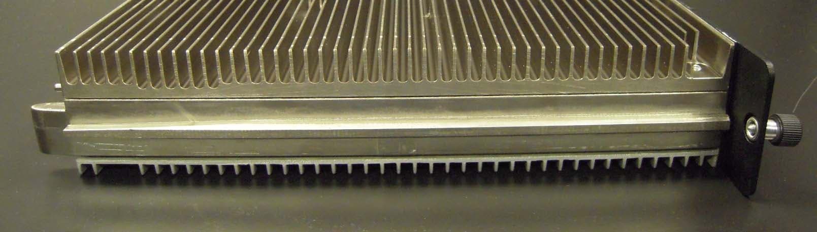
M External Photos Exhibit Global Telecom Solutions Sector FCC ID: IHET5EJ1 FCC Filing – SC480 1X-EVDO with cPAs @ 800MHz CDMA BTS Page 1 of 9 External Photos Exhibit SC480 1X-EVDO with cPAs @ 800MHz CDMA BTS Number Description 1 Front View Compact 2 Rear View Compact 3 Left Side View Compact 4 Right Side View Compact 5 Top View Compact 6 Front View cPA 7 Rear View cPA 8 Rear View cPA (No cover) M External Photos Exhibit Global Telecom Solutions Sector FCC ID: IHET5EJ1 FCC Filing – SC4801X-EVDO with cPAs @ 800MHz CDMA BTS Page 2 of 9 External Photos Exhibit Compact – Front View M External Photos Exhibit Global Telecom Solutions Sector FCC ID: IHET5EJ1 FCC Filing – SC480 1X-EVDO with cPAs @ 800MHz CDMA BTS Page 3 of 9 External Photos Exhibit Compact – Rear View M External Photos Exhibit Global Telecom Solutions Sector FCC ID: IHET5EJ1 FCC Filing – SC480 1X-EVDO with cPAs @ 800MHz CDMA BTS Page 4 of 9 External Photos Exhibit Compact – Left Side View M External Photos Exhibit Global Telecom Solutions Sector FCC ID: IHET5EJ1 FCC Filing – SC480 1X-EVDO with cPAs @ 800MHz CDMA BTS Page 5 of 9 External Photos Exhibit Compact – Right Side View M External Photos Exhibit Global Telecom Solutions Sector FCC ID: IHET5EJ1 FCC Filing – SC480 1X-EVDO with cPAs @ 800MHz CDMA BTS Page 6 of 9 External Photos Exhibit Compact – Top View M External Photos Exhibit Global Telecom Solutions Sector FCC ID: IHET5EJ1 FCC Filing – SC480 1X-EVDO with cPAs @ 800MHz CDMA BTS Page 7 of 9 External Photos Exhibit cPA – Front View M External Photos Exhibit Global Telecom Solutions Sector FCC ID: IHET5EJ1 FCC Filing – SC480 1X-EVDO with cPAs @ 800MHz CDMA BTS Page 8 of 9 Internal Photos Exhibit cPA - Rear View M External Photos Exhibit Global Telecom Solutions Sector FCC ID: IHET5EJ1 FCC Filing – SC480 1X-EVDO with cPAs @ 800MHz CDMA BTS Page 9 of 9 Internal Photos Exhibit cPA - Front View (no cover)
ID Label/Location Info
IHET5EJ1 US: IHEDENANSC4801XDO Applicant: Motorola FCC ID IHET5EJ1 Applicant: Motorola FCC ID IHET5EJ1 FCC LABELS placed here with front panels removed
Internal Photos
M Internal Photos Exhibit Global Telecom Solutions Sector FCC ID: IHET5EJ1 FCC Filing – SC480 1X-EVDO with cPAs @ 800MHz CDMA BTS Page 1 of 18 Internal Photos Exhibit CMPC – Front View M Internal Photos Exhibit Global Telecom Solutions Sector FCC ID: IHET5EJ1 FCC Filing – SC480 1X-EVDO with cPAs @ 800MHz CDMA BTS Page 2 of 18 Internal Photos Exhibit CMPC - Rear View M Internal Photos Exhibit Global Telecom Solutions Sector FCC ID: IHET5EJ1 FCC Filing – SC480 1X-EVDO with cPAs @ 800MHz CDMA BTS Page 3 of 18 Internal Photos Exhibit Group Line Interface (GLI3) - Front View M Internal Photos Exhibit Global Telecom Solutions Sector FCC ID: IHET5EJ1 FCC Filing – SC480 1X-EVDO with cPAs @ 800MHz CDMA BTS Page 4 of 18 Internal Photos Exhibit Group Line Interface (GLI3) - Rear View M Internal Photos Exhibit Global Telecom Solutions Sector FCC ID: IHET5EJ1 FCC Filing – SC480 1X-EVDO with cPAs @ 800MHz CDMA BTS Page 5 of 18 Internal Photos Exhibit BBX-1X - Front View M Internal Photos Exhibit Global Telecom Solutions Sector FCC ID: IHET5EJ1 FCC Filing – SC480 1X-EVDO with cPAs @ 800MHz CDMA BTS Page 6 of 18 Internal Photos Exhibit BBX-1X - Rear View M Internal Photos Exhibit Global Telecom Solutions Sector FCC ID: IHET5EJ1 FCC Filing – SC480 1X-EVDO with cPAs @ 800MHz CDMA BTS Page 7 of 18 Internal Photos Exhibit MCC-1X - Front View M Internal Photos Exhibit Global Telecom Solutions Sector FCC ID: IHET5EJ1 FCC Filing – SC480 1X-EVDO with cPAs @ 800MHz CDMA BTS Page 8 of 18 Internal Photos Exhibit MCC-1X - Rear View M Internal Photos Exhibit Global Telecom Solutions Sector FCC ID…
Text truncated - open the document above for the full version.
Contact Information
Applicant
Steve Mitchell
Technical Contact
MotorolaTerry Schwenk
[email protected]1-847-435-0780
1475 W. Shure Drive · Arlington Heights, Illinois · United States
Non-Technical Contact
MotorolaFrancisco Avalos
1-847-632-9743
Test Firm
Underwriters Laboratories Inc.Rick Titus
Technical Specifications
| # | Rule Parts | Frequency Range | Power Output | Emission | Tolerance |
|---|---|---|---|---|---|
| 1 | 22H | 869.7 MHz - 893.31 MHz | 20 W | 1M30F9W | 1.5000000000 ppm |
Other Applications from Nokia Solutions and Networks
IHET4KJ1
Apr 28, 2010LTE 700 MHz Public Safety Base Station Transceiver
Equipment Class
TNB - Licensed Non-Broadcast Station Transmitter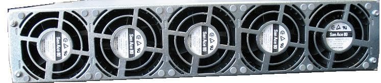
IHET5GX1
Oct 14, 2007UBS CDMA XMI Transceiver at 800 MHz
Equipment Class
TNB - Licensed Non-Broadcast Station Transmitter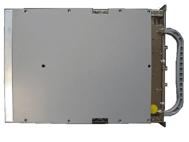
IHET6HG1
Sep 12, 2007CDMA Base Station
Equipment Class
PCB - PCS Licensed Transmitter
IHET7HN1
Jul 17, 20072.5 GHz Diversity Access Point
Equipment Class
TNB - Licensed Non-Broadcast Station Transmitter
IHET7GT1
Jan 14, 20072.5GHz DIVERSITY ACCESS POINT
Equipment Class
TNB - Licensed Non-Broadcast Station Transmitter