J3OWDAP5000LAN Access Point
Xircom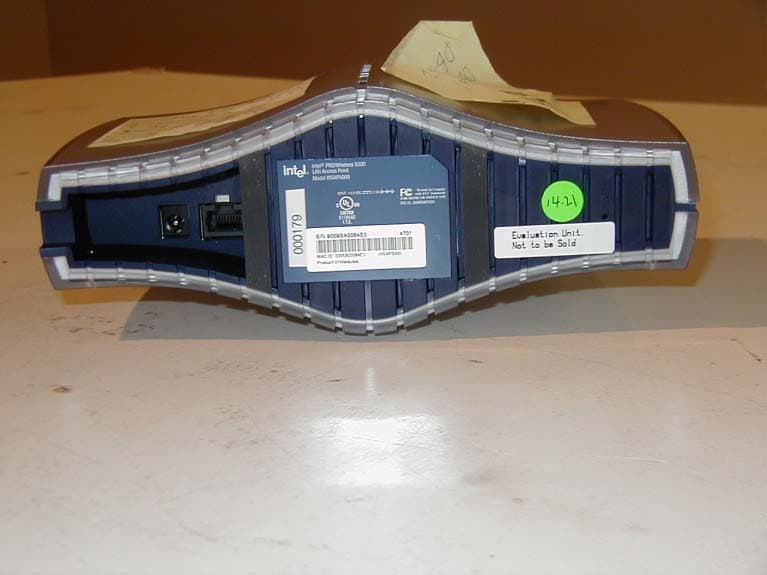
Click to zoom
Application Details
- Equipment Class
- DSS - Part 15 Spread Spectrum Transmitter
- Date of Grant
- May 28, 2002
- Application Purpose
- Original Equipment
- Date of Application
- May 15, 2002
- Equipment Note
- LAN Access Point
- Frequency Range
- 2412.00000000 - 2462.00000000
- Company
- Xircom
- Country
- United States
Documents & Files
Document Text
Text extracted from the exhibit documents filed with the FCC. Open a document above to read the original.
Users Manual
1 Overview Welcome to the Intel® PRO/Wireless 5000 LAN Access Point User's Guide. This guide covers software installation, configuration, and troubleshooting. To select a topic, click a link in the contents column to the left. After installing the access point register your access point online. Go to the Intel Product Registration Web site. Copyright © 2002 Intel Corporation. Legal Information Introduction The 802.11a and 802.11b Intel® PRO/Wireless 5000 LAN Dual Access Point operates in the both 5 GHz and 2.4 GHz environment at speeds up to 54 Mbps (802.11a) and 11 Mbps (802.11b). It features a software configurable antenna and will supports IEEE 802.3af Power over Ethernet. Each access point uses eight non-overlapping transmission channels for support of up to 64 active users per access point. Placement can be on a desk or table, mounting on a wall or ceiling. The PRO/Wireless 5000 LAN Access Point is compatible with other products supporting the IEEE 802.11a standard and 802.11b standard. Security features include support for 128, 64, and 0-bit Wired Equivalent Privacy (WEP) encryption and Virtual Private Network (VPN) compatibility. A browser-based user interface is provided for configuration of the access point. See the installation instructions for information on how to set up and configure one or more access points. For information on how to set up a wireless LAN, see the Administrator's Guide . The Administrator's Guide is intended for use by network administrators. 802.1x Authentication The 802.11a Intel® PRO/Wireless 5000 LAN Dual Access Point supports 802.1x authentication for Windows operating systems. 802.1x authentication for wireless LANs has three main components: The supplicant (usually the client software); the authenticator (the access point); and the authentication server (usually a Remote Authentication Dial-In User Service or RADIUS server). 802.1x is a standards-based solution for port-level authentication for a wired or wireless Ethernet client systems. Copyright © 2002 Intel Corporation. Legal Information 2 Installation • Introduction • Installation Options and Requirements • Connect and Power Up the Access Point • LED Indicators • Configuring the Access Point for the First Time • Using DHCP • Access Point Default Values • Restore Factory Defaults • Select a Location for Installation of the Access Point • Access Point Configuration Introduction Your Intel® PRO/Wireless 5000 LAN Access Point, when used with Intel PRO/Wireless 5000 LAN Adapters or other 802.11a and 802.11b-compliant wireless LAN adapters, offers an easy and economical way to add secure wireless connectivity to a wired local area network (LAN) within a building or office. For detailed hardware installation requirements and diagrams, see the printed Quick Installation Guide supplied with the access point. Installation Options and Requirements Review the following options and requirements for installation and configuration of the access point for connection over the wired LAN: • (Recommended) For configuration of the access point, you will need a wired client workstation connected to the access point directly (recommended) or over the wired LAN to which the access point is connected. Note: Initial setup and configuration must be done over a wired connection, but subsequent changes to the configuration can be done over a wireless connection. • (Optional) DHCP server support for automatic assignment of an IP address to the access point over the wired network. You can configure the access point to use DHCP to get its IP address. See Using DHCP . Connect and Power Up the Access Point Connect the Access Point to the Wired Network • Plug an RJ-45 Category 5 Ethernet cable into the RJ-45 connector on the bottom of the access point and into a 10/100 Ethernet wall connector or hub. 3 Connect the Access Point to a Source of AC Power • Plug the power adapter into a wall outlet. • Plug the power adapter cable into the power socket on the bottom of the access point. LED Indicators Once the access point is connected to a wired network and is powered on, check the LED indicators to verify that the unit is functioning correctly. If the access point fails to initialize, restart it by disconnecting and reconnecting the power. The Intel® PRO/Wireless 5000 LAN Access Point can be mounted "right side up" on a desk or table or "upside down" on a wall or ceiling. The LED discussion that follows is based on a wall- or ceiling-mounted configuration in which the access point is "upside down." In this configuration the "Ready" LED will be the top LED and "Wired link" will be the bottom LED. • The "Ready" LED should be lit. • If the access point is connected to a LAN through an Ethernet cable, the "Wired link" LED should be lit (green for 10 Mbps, orange for 100 Mbps) and the "Wired network activity" LED should be blinking. • If the access point is communicating with a wireless adapter, the "Wireless radio activity" LED should be flashing steadily. The Wireless radio activity LED blinks faster when the access point is sending or receiving information from a wireless adapter. • Note that there are two sets of LEDs for "Wireless radio activity" and "Wireless radio association." The description indicates which models use which set or sets. Viewed on a wall- or ceiling-mounted access point, the LED indicators have the following locations and functions. Ready Green. This indicator will stay illuminated after the access point has completed the initialization sequence. The Ready light flashes quickly 3 times during a reset to factory default settings . Wireless radio activity (802.11a) Yellow flashes steadily if no adapter associated, and more rapidly when transferring data. Applies to models WSAP5000 and WDAP5000. Wireless radio association (802.11a) Green will be ON if a client is associated to the access point and OFF if not. Applies to models WSAP5000 and WDAP5000. Wireless radio activity (802.11b) Yellow flashes steadily if no ada…
Text truncated - open the document above for the full version.
Cover Letter(s)
File: R47112 April 30, 2002 Chief, Equipment Authorization Branch, Authorization and Evaluation Division, Office of Engineering and Technology FEDERAL COMMUNICATIONS COMMISSION P.O. Box 358315 Pittsburgh, PA 15251-5315 Gentlemen: The enclosed documents constitute a formal submittal and application for a Grant of Equipment Authorization pursuant to Subpart C of Part 15 of FCC Rules (CFR 47) regarding intentional radiators. Data within this report demonstrates that the equipment tested complies with the FCC limits for intentional radiators. Elliott Laboratories, as duly authorized agent prepared this submittal. A copy of the letter of our appointment as agent is enclosed. If there are any questions or if further information is needed, please contact Elliott Laboratories for assistance. Sincerely, Juan Martinez Senior EMC Engineer JM/jls Enclosures: Application Fee FCC Form 159 FCC Form 731 Agent Authorization Letter Emissions Test Report with Exhibits
External Photos
Front Side of the Dual Accesspoint (WDAP5000) Back side of the Dual Accesspoint (WDAP5000) Bottom Side of the Dual Accesspoint (WDAP5000)
ID Label/Location Info
A/W #832-2286-001A Master WDAP5000 FAB #830-1761-001 ECN 24450 Approved by IDA for use in Singapore. DBxxxxx HHHHAAAA-FFFF Intel ® PRO/Wireless 5000 LAN Dual Access Point Model WDAP5000 .65" R-LARN-01-0202 C US LISTED E178682 E178682 I.T.E.I.T.E. U L 90LP0011 INPUT: + 5.0 VDC 2.5A This device complies with Part 15 of the FCC Rules. Operation is subject to the following two conditions: (1) This device may not cause harmful interference, and (2) This device must accept any interference received, including interference that may cause undesired operation FCC ID: J30WDAP5000 CANADA ICES/NMB-003 Class/Classe (B) CANADA: xxxxxxxxxxA SCT TTDXIMXXX-XXX CNC XX-XXXX 01WYBA1010 D02-0017JP WM3A5000DAP Printed By: Robert PaxmanReference Only unless DC stampedDate Printed: 07-Nov-2001 11:49:12 Number: 835-0115-001Rev: 01 23881Status: Prototype
Internal Photos
Internal Picture with partial assembly Front Side LED (Exterior Shield) Half shield removed, exposing the Front Side of AP Motherboard (LED Side) Front Side of AP motherboard showing the 2.4 GHz Mini PCI card and interconnection to antenna. Back Side of AP Motherboard showing the 5 GHz Mini PCI card and interconnection to antenna 2.4 GHz MINI PCI card front side with shield 2.4 GHz Mini PCI card front side with shield removed 2.4 GHz Mini PCI card back side Front Side of AP Motherboard (LED Side) were the 2.4 GHz Mini PCI will be installed Back side of AP motherboard were the 5 GHz Mini PCI will be installed Front Side of Antenna Back Side of Antenna
RF Exposure Info
Technical Specification Sheet 5GHz 802.11a Antenna – 100-0932-001 General Description This dual band, 2.4GHz and 5.2GHz, antenna has been designed specifically for the WDAP5000 Access Product. It features 802.11a active antenna elements and 802.11b passive elements. The 802.11a antenna has two different emission patterns selectable via software control, omni and front half circle. To connect to the 802.11a active elements a 2mm UMP connector is used. A coaxial UFL connector is used to feed each of the 802.11b elements. Electrical Specifications 802.11a Array Frequency Range: 5.15 – 5.35 GHz Peak Gain: 1.8dBi Omni, 5.6dBi Pattern VSWR: less than 2.0:1 Polarization: Circular/Universal Azimuth Beam-width: Omni-directional/Pattern Power Handling: 10Watt CW Feed Point Impedance: 50 OHMS unbalanced 802.11b Elements Frequency Range: 2.41 – 2.49 GHz Peak Gain: 6.2dBi VSWR: less than 2.0:1 Polarization: Linear Azimuth Beam-width: Omni-directional Power Handling: 10Watt CW Feed Point Impedance: 50 OHMS unbalanced Mechanical Specifications Size: 6.378 x 2.467 x 0.123 Inches Weight: 1.5 oz Mounting: Snap on 12 pin Connector and slots
RF Exposure Info
Introduction FCC part 1.1310, Table 1 limits the power density for uncontrolled exposure to 1mW/cm 2 . The power density, Pd (mW/cm 2 ) at a distance d (cm) for an EIRP of Pt (mW) is given in the following equation: Pd = Pt/(4πd 2 ) The AccessPoint is designed to be a mobile device, with a minimum separation from persons of 20cm. The following calculations demonstrate that the device, when installed and operated as intended, will meet the FCC’s requirements for uncontrolled exposure at a distance of 20cm: 5GHz MINI PCI: The 5GHz mini PCI card installed in the AccessPoint can use the internal antennas configured to give either a 1.8dBi omni-pattern or a 5.6 dBi Half-round pattern. The maximum output power for the 5 GHz Mini PCI is 21 dBm. The EIRPs for these two configurations are, therefore: 1.8 dBi + 21 dBm = 22.8 dBm (190 mW EIRP) 5.6 dBi + 21 dBm = 26.6 dBm (457 mW EIRP) The power spectral density at 20cm for the two different antenna configurations are: Pd = 190/(4π20 2 ) = 0.038 mW/cm² (Omni antenna) Pd = 457/(4π20 2 ) = 0.091 mW/cm² (Half-round antenna) 2.4 GHz MINI PCI: The 2.4GHz mini PCI card installed in the AccessPoint uses an internal antenna with a gain of 6.2 dBi. The maximum output power from the 2.4GHz device is 15.3dBm. The EIRP from the mini PCI card’s antenna is, therefore: 6.2 dBi + 15.3 dBm = 21.5 dBm (141 mW EIRP) The power spectral density at 20cm for this EIRP is, therefore: Pd = 141/(4π20 2 ) = 0.028 mW/cm² Co-located Transmitters: The total power density at a distance from 20cm from the AccesPoint product with both the 2.4GHz and 5GHz devices operational is the sum of the power densities from each device The worst-case (highest) power density from the 5GHz device is when it is configured to use the half-round antenna. The total power spectral density with the 5GHz device operating using the half- round antenna and the 2.4GHz device operational is, therefore: 0.091 mW/cm² + 0.028 mW/cm² = 0.119 mW/cm² The calculated value for the power spectral density at 20cm is lower than the maximum permitted density of 1 mW/cm². Note: RF Warning statement in page 15 of 27 has been place in the user manual.
Test Report
File: R47112 Page 1 of 15 Electromagnetic Emissions Test Report and Application for Grant of Equipment Authorization pursuant to FCC Part 15, Subpart C Specifications for an Intentional Radiator on the Intel Corporation Models: WDAP5000, WSAP2000, and WSAP5000 FCC ID: J3OWDAP5000 GRANTEE: Intel Corporation 2300 Corporate Center Drive Thousand Oaks, CA 91320 TEST SITE: Elliott Laboratories, Inc. 684 W. Maude Avenue Sunnyvale, CA 94086 REPORT DATE: April 30, 2002 FINAL TEST DATE: January 21, 2002 AUTHORIZED SIGNATORY: ______________________________ Juan Martinez Senior EMC Engineer This report shall not be reproduced, except in its entirety, without the written approval of Elliott Laboratories, Inc. Elliott Laboratories, Inc. -- EMC Department Test Report Report Date: April 30, 2002 File: R47112 Page 2 of 15 Pages TABLE OF CONTENTS COVER PAGE..................................................................................................................................................................................1 TABLE OF CONTENTS...............................................................................................................................................................2 SCOPE.............................................................................................................................................................................................3 OBJECTIVE...................................................................................................................................................................................3 STATEMENT OF COMPLIANCE..............................................................................................................................................3 EMISSION TEST RESULTS.......................................................................................................................................................4 LIMITS OF CONDUCTED INTERFERENCE VOLTAGE..................................................................................................4 LIMITS OF ANTENNA CONDUCTED POWER...................................................................................................................4 LIMITS OF RADIATED INTERFERENCE FIELD STRENGTH........................................................................................4 LIMITS OF POWER AND BANDWIDTH...............................................................................................................................5 MEASUREMENT UNCERTAINTIES.....................................................................................................................................5 EQUIPMENT UNDER TEST (EUT) DETAILS..........................................................................................................................6 GENERAL..................................................................................................................................................................................6 ENCLOSURE.............................................................................................................................................................................6 MODIFICATIONS.....................................................................................................................................................................7 SUPPORT EQUIPMENT.........................................................................................................................................................7 EXTERNAL I/O CABLING.......................................................................................................................................................7 EUT OPERATION DURING EMISSIONS.............................................................................................................................7 TEST SITE......................................................................................................................................................................................8 GENERAL INFORMATION.....................................................................................................................................................8 RADIATED EMISSIONS CONSIDERATIONS.....................................................................................................................8 MEASUREMENT INSTRUMENTATION..................................................................................................................................9 INSTRUMENT CONTROL COMPUTER...............................................................................................................................9 LINE IMPEDANCE STABILIZATION NETWORK (LISN).................................................................................................9 POWER METER........................................................................................................................................................................9 FILTERS/ATTENUATORS.....................................................................................................................................................10 ANTENNAS..............................................................................................................................................................................10 ANTENNA MAST AND EQUIPMENT TURNTABLE........................................................................................................10 INSTRUMENT CALIBRATION.............................................................................................................................................10 TEST PROCEDURES.................................................................................................................................................................11 EUT AND CABLE PLACEMENT........................................................................................…
Text truncated - open the document above for the full version.
Test Report
Report pages location for the Power Output, Spectral density, 6-dB Bandwidth, Out-of-Band emissions data for the 2.4 GHz Mini PCI card. 6-dB Bandwidth (Page 20 of 23) Test Procedure 6-dB Bandwidth Data Plots are located in 56 of 92 of the complete Report Peak Output Power (Page 20 of 23) Test Procedure Power Output Data is located in 60 of 92 of the complete Report Spectral Density Output (Page 20 of 23) Test Procedure Spectral Density Data Plots are located in 62 of 92 of the complete Report RF Antenna Conducted Test (Page 21 of 23) Test Procedure RF Antenna Conducted Data Plots are located in 66 of 92 of the complete Report Processing Gain (A separate report label “Processing Gain”
Test Report
FCC ID: M3AWEB56GA Report Number: B11108D1 114 OLINDA DRIVE, BREA, CALIFORNIA 92823 PHONE: (714) 579-0500 FAX: (714) 579-1850 Page 1 of 23 FCC PART 15, SUBPART C TEST METHOD: ANSI C63.4-1992 for MPCI TYPE 3A 802.11B WIRELESS + V.92 MODEM CARD Model: M3AWEB56GA Prepared for XIRCOM, INC. 2300 CORPORATE CENTER DRIVE THOUSAND OAKS, CALIFORNIA 91320 COMPATIBLE ELECTRONICS INC. 114 OLINDA DRIVE BREA, CALIFORNIA 92823 (714) 579-0500 DATE: NOVEMBER 13, 2001 REPORT APPENDICES TOTAL BODY A B C D PAGES 23 2 2 14 51 92 This report shall not be reproduced except in full, without the written approval of Compatible Electronics. FCC ID: M3AWEB56GA Report Number: B11108D1 114 OLINDA DRIVE, BREA, CALIFORNIA 92823 PHONE: (714) 579-0500 FAX: (714) 579-1850 Page 2 of 23 TABLE OF CONTENTS Section / Title PAGE GENERAL REPORT SUMMARY 4 1. PURPOSE 6 2. ADMINISTRATIVE DATA 7 2.1 Location of Testing 7 2.2 Traceability Statement 7 2.3 Cognizant Personnel 7 2.4 Date Test Sample was Received 7 2.5 Disposition of the Test Sample 7 2.6 Abbreviations and Acronyms 7 3. APPLICABLE DOCUMENTS 8 4. Description of Test Configuration 9 4.1 Description of Test Configuration - EMI 9 4.1.1 Cable Construction and Termination 10 5. LISTS OF EUT, ACCESSORIES AND TEST EQUIPMENT 11 5.1 EUT and Accessory List 11 5.2 EMI Test Equipment 12 6. TEST SITE DESCRIPTION 14 6.1 Test Facility Description 14 6.2 EUT Mounting, Bonding and Grounding 14 7. CHARACTERISTICS OF THE TRANSMITTER 15 7.1 Transmitter Power 15 7.2 Channel Number and Frequencies 15 7.3 Chipping Rate 15 7.4 Spreading Gain 15 7.5 Antenna Gain 15 7.6 Processing Gain 16 8. Test Procedures 17 8.1 RF Emissions 17 8.1.1 Conducted Emissions Test 17 8.1.2 Radiated Emissions (Spurious and Harmonics) Test 18 8.2 6 dB Bandwidth for Direct Sequence Systems 20 8.3 Peak Output Power 20 8.4 Spectral Density Output 20 8.5 RF Antenna Conducted Test 21 8.6 RF Band Edges 21 8.7 Processing Gain 22 9. CONCLUSIONS 23 FCC ID: M3AWEB56GA Report Number: B11108D1 114 OLINDA DRIVE, BREA, CALIFORNIA 92823 PHONE: (714) 579-0500 FAX: (714) 579-1850 Page 3 of 23 LIST OF APPENDICES APPENDIX TITLE A Modifications to the EUT B Additional Models Covered Under This Report C Diagrams, Charts and Photos • Test Setup Diagrams • Radiated and Conducted Emissions Photos • Antenna and Effective Gain Factors D Data Sheets LIST OF FIGURES FIGURE TITLE 1 Conducted Emissions Test Setup 2 Plot Map And Layout of Test Site FCC ID: M3AWEB56GA Report Number: B11108D1 114 OLINDA DRIVE, BREA, CALIFORNIA 92823 PHONE: (714) 579-0500 FAX: (714) 579-1850 Page 4 of 23 GENERAL REPORT SUMMARY This electromagnetic emission test report is generated by Compatible Electronics Inc., which is an independent testing and consulting firm. The test report is based on testing performed by Compatible Electronics personnel according to the measurement procedures described in the test specifications given below and in the "Test Procedures" section of this report. The measurement data and conclusions appearing herein relate only to the sample tested and this report may not be reproduced without the written permission of Compatible Electronics, unless done so in full. This report must not be used to claim product endorsement by NVLAP or any other agency of the U.S. Government. Device Tested: MPCI Type 3A 802.11B Wireless + V.92 Modem Card Model: M3AWEB56GA S/N: N/A Modifications: The EUT was not modified in order to meet the specifications. Manufacturer: Xircom, Inc. 2300 Corporate Center Drive Thousand Oaks, California 91320 Test Date: November 8, 2001 File # For Canada IC2154-D Test Specifications : EMI requirements FCC Title 47, Part 15 Subpart B; and Subpart C, sections 15.205, 15.207, 15.209, and 15.247 Test Procedure: ANSI C63.4: 1992 Test Deviations: The test procedure was not deviated from during the testing. FCC ID: M3AWEB56GA Report Number: B11108D1 114 OLINDA DRIVE, BREA, CALIFORNIA 92823 PHONE: (714) 579-0500 FAX: (714) 579-1850 Page 5 of 23 SUMMARY OF TEST RESULTS TEST DESCRIPTION RESULTS 1 Conducted RF Emissions, 450 kHz – 30 MHz Complies with the relevant requirements of FCC Title 47, Part 15, Subpart C, section 15.207 2 Spurious Radiated RF Emissions, 10 kHz – 25000 MHz Complies with the relevant requirements of FCC Title 47, Part 15, Subpart C, section 15.247(c) 3 Fundamental and Emissions produced by the intentional radiator in non-restricted bands, 10 kHz – 25 GHz Complies with the relevant requirements of FCC Title 47, Part 15, Subpart C, section 15.247(c) 4 Emissions produced by the intentional radiator in restricted bands, 10 kHz – 25 GHz Complies with the relevant requirements of FCC Title 47, Part 15, Subpart C, section 15.205 and 15.209(a) 5 6 dB Bandwidth Complies with the relevant requirements of FCC Title 47, Part 15, Subpart C, section 15.247 (a)(2) 6 Maximum Peak Output Power Complies with the relevant requirements of FCC Title 47, Part 15, Subpart C, section 15.247 (b)(1) 7 RF Antenna Conducted Complies with the relevant requirements of FCC Title 47, Part 15, Subpart C, section 15.247 (c) 8 Peak Power Spectral Density Conducted from the Intentional Radiator to the Antenna Complies with the relevant requirements of FCC Title 47, Part 15, Subpart C, section 15.247 (d) 9 Processing Gain Complies with the relevant requirements of FCC Title 47, Part 15, Subpart C, section 15.247 (e) FCC ID: M3AWEB56GA Report Number: B11108D1 114 OLINDA DRIVE, BREA, CALIFORNIA 92823 PHONE: (714) 579-0500 FAX: (714) 579-1850 Page 6 of 23 1. PURPOSE This document is a qualification test report based on the Electromagnetic Interference (EMI) tests performed on the MPCI Type 3A 802.11B Wireless + V.92 Modem Card Model: M3AWEB56GA. Only the RF module itself is being approved. The EMI measurements were performed according to the measurement procedure described in ANSI C63.4: 1992. The tests were performed in order to determine whether the electromagnetic emissions from the MPCI Type 3A 802.11B Wireless + V.92 Modem Card, referred to as EUT hereafter,…
Text truncated - open the document above for the full version.
Test Report
FCC Processing Gain report of Intersil MiniPCI 2.4 GHz WLAN transceiver model ISL37400M for: -channel 1 at 11Mbps -channel 6 at 2 Mbps -channel 6 at 11 Mbps -channel 11 at 11 Mbps intersil PRISM radio Jamming Margin Test _________________________________________________________________________________________________________ _____________________________________________________________________________________ intersil Page 1 Testing for compliance with FCC rules 15-247e Carl Andren intersil Corporation [email protected] 321-724-7535 Scope This report presents the test procedure, test configuration and test data associated with a FCC Part 15.247 (e) Jamming Margin test for the indirect measurement of processing gain. Applicable Reference Documents. 1. ìOperation within the bands 902-928 MHz, 2400-2483.5, and 5725-5850 MHzî Title 47 Part 15 section 247 (e) Code of Federal Regulations. (47 CFR 15.247). 2. ìReport and Order: Amendment of Parts 2 and 15 of the Commissionís Rules Regarding Spread Spectrum Transmitters. Appendix C: ëGuidance on Measurements for Direct Sequence Spread Spectrum Systemsî FCC 97-114. ET Docket No. 96-8, RM-8435, RM-8608, RM-8609. 3. ìISL3874 Direct Sequence Spread Spectrum Baseband Processor 4. ì M-ary Orthogonal Keying BER Curveî, Test Background and Procedure. According to FCC regulations [1], a direct sequence spread spectrum system must have a processing gain, G p of at least 10 dB. Compliance to this requirement can be shown by demonstrating a relative bit-error-ratio (BER) performance improvement (and corresponding signal to noise ratio per symbol improvement of at least 10 dB) between the case where spread spectrum processes (coding, modulation) are engaged relative to the processes being bypassed. In some practical systems, the spread spectrum processing cannot simply be bypassed. In these cases, the processing gain can be indirectly measured by a jamming margin test [2]. In accordance with the new NPRM 99-231, if the vendor has a system with less than 10 chips per symbol, the CW jamming results must be supported by a theoretical explanation of the system processing gain. intersil PRISM radio Jamming Margin Test _________________________________________________________________________________________________________ _____________________________________________________________________________________ intersil Page 2 Theoretical calculations The processing gain is related to the jamming margin as follows [2]: system output p L S J N S G+ + = Where BER REFERENCE is the reference bit error ratio with its corresponding, theoretical output signal to noise ratio per symbol, (S/N) output , (J/S) is the jamming margin (jamming signal power relative to desired signal power), and L system are the system implementation losses. The maximum allowed total system implementation loss is 2 dB. The ISL3874 direct sequence spread spectrum baseband processor uses CCK modulation which is a form of M-ary Orthogonal Keying. The BER performance curve is given by [5]: ì The probability of error for generalized M-ary Orthogonal signaling using coherent demodulation is given by: PPQz E z dz ec b M S N =− =−−+ − − − ∞ ∫ 11 1 2 212 2 1 2 1 2 01 0 π η ()exp This integral cannot be solved in closed form, and numerical integration must be used. This is done in a MATHCAD environment and is displayed in graphical format. intersil PRISM radio Jamming Margin Test _________________________________________________________________________________________________________ _____________________________________________________________________________________ intersil Page 3 1.1 1000 byte PER vs. Es/No 15.51616.517 10 -2 10 -1 10 0 11 Mbps CCK in Thermal Noise Es/No (dB) 1000 byte Packet Error Rate The reference PER is specified as 8% . The corresponding Es/No (signal to noise ratio per symbol) is 16.4 dB. The Es/No required to achieve the desired BER with maximum system implementation losses is 18.4 dB. The minimum processing gain is again, 10 dB, therefore: dB S J dBdBL S J N E G system output o s p 100.24.16≥ ++=+ + = dB S J dBG p 104.18≥ += The minimum jammer to signal ratio is as follows: dB S J 4.8−≥ For the case of the ISL3874, the bit rates are 1, 2, 5.5, and 11 Mbps. The corresponding symbol rates are 1, 1, 1.375, and 1.375 MSps. The chip rate is always 11 MCps, so the ratio of chip rate to symbol rate is 11:1 for the 1 and 2 Mbps rates and 8:1 for the 5.5 and 11 Mbps rates. Since the symbol rate to bit rate is less than 10 for the higher rates, we supply the theoretical processing gain calculation for these cases where both spread spectrum intersil PRISM radio Jamming Margin Test _________________________________________________________________________________________________________ _____________________________________________________________________________________ intersil Page 4 processing gain and coding gain are utilized. This is reasonable in that they cannot be separated in the demodulation process. If a separable FEC coding scheme were used, we would not be comfortable making this assertion. As can be seen from the curve of figure 1, the Es/N0 is 16.4 dB at the PER of 8%. This PER can be related to a BER of 1e-5 on 1000 byte packets. With 8 bits per symbol, the Eb/N0 is then 7.4 …
Text truncated - open the document above for the full version.
Contact Information
Applicant
Robert W. Paxman(Compliance Engineer)
Technical Contact
Elliott Laboratories, Inc.Juan Martinez
[email protected]408-245-7800
684 W. Maude Ave · Sunnyvale, California · United States
Test Firm
Elliott Laboratories LLCDavid Bare
Technical Specifications
| # | Rule Parts | Frequency Range | Power Output |
|---|---|---|---|
| 1 | 15C | 2.41 GHz - 2.46 GHz | 34.00 mW |
Other Applications from Xircom
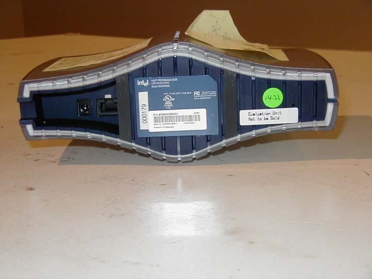
J3OWSAP2000
Jun 09, 2002WLAN Accesspoint
Equipment Class
DSS - Part 15 Spread Spectrum Transmitter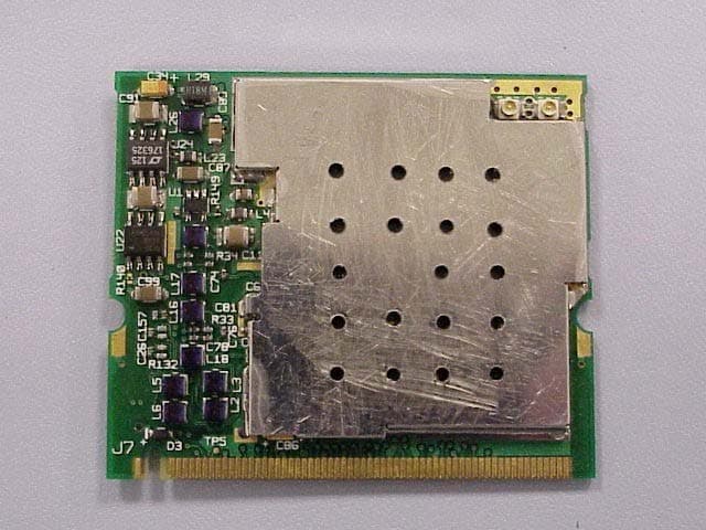
J3OWM3A5000
May 23, 2002Mini PCI Card
Equipment Class
NII - Unlicensed National Information Infrastructure TX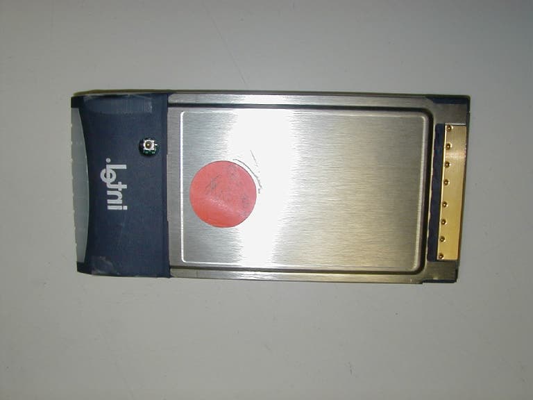
J3OWCB5000A
Apr 18, 2002Intel PRO/ Wireless 5000 Cardbus Adapter
Equipment Class
NII - Unlicensed National Information Infrastructure TX
J3OWPCI5000
Mar 26, 2002Wreless PCI Adapter
Equipment Class
NII - Unlicensed National Information Infrastructure TX
J3OM3AWEB56GA
Dec 25, 2001Spread Spectrum PCI Card Transceiver Module
Equipment Class
DSS - Part 15 Spread Spectrum Transmitter