J9C-65VE239P2WLAN a/b/g/n PCIe minicard Adapter
Qualcomm Technologies, Inc.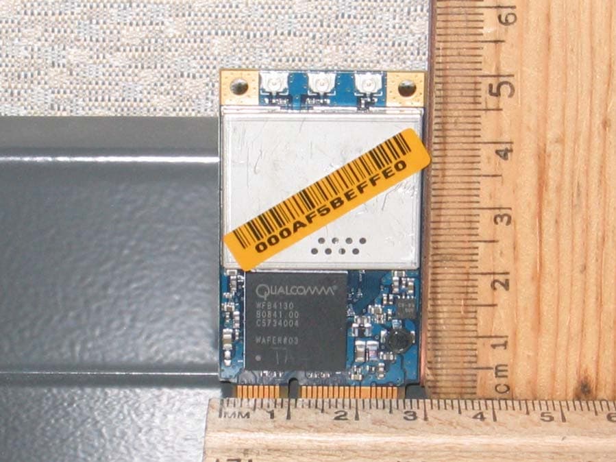
Click to zoom
Application Details
- Equipment Class
- DTS - Digital Transmission System
- Date of Grant
- Oct 17, 2007
- Application Purpose
- Original Equipment
- Date of Application
- Oct 17, 2007
- Equipment Note
- WLAN a/b/g/n PCIe minicard Adapter
- Frequency Range
- 5755.00000000 - 5795.00000000
- Company
- Qualcomm Technologies, Inc.
- Country
- United States
Documents & Files
Document Text
Text extracted from the exhibit documents filed with the FCC. Open a document above to read the original.
Users Manual
Installation and User Guide: WFB400 Windows Wireless LAN Client March 2007 Installation and User Guide WFB400 Windows Wireless LAN Client Adapters Copyright © 2007 by QUALCOMM, Inc. All Rights Reserved. No part of this work may be reproduced, stored in a retrieval system, or transmitted in any form or by any means, electronic, mechanical, photocopying, recording, or otherwise, without the prior written permission of unless such copying is expressly permitted by U.S. copyright law. Page 2 of 29 Installation and User Guide: WFB400 Windows Wireless LAN Client Contents CONTENTS .................................................................................................................................................................3 PREFACE ....................................................................................................................................................................4 OVERVIEW ................................................................................................................................................................6 Device Types...................................................................................................................................................6 Shipping Package Contents.......................................................................................................................6 System Requirements.................................................................................................................................6 Inserting and Removing the Wireless LAN Client Adapter.............................................................6 Checking Adapter Activity ............................................................................................................................................... 7 Installing the Wireless LAN Client Adapter Driver............................................................................7 Installation Steps ............................................................................................................................................................... 7 Confirming the Installation........................................................................................................................9 Verifying the Installation — Windows XP ..................................................................................................................... 10 Uninstalling the Windows Wireless Drivers.......................................................................................12 INTRODUCTION TO WIRELESS ZERO CONFIGURATION .........................................................................14 Service Set Identifiers...............................................................................................................................14 Wireless Bands and Channels.................................................................................................................14 WZC Overview..............................................................................................................................................15 Accessing WZC.............................................................................................................................................15 Wireless Security.........................................................................................................................................18 CONFIGURATION OVERVIEW ...........................................................................................................................20 REGULATORY ........................................................................................................................................................22 GLOSSARY ...............................................................................................................................................................23 INDEX ........................................................................................................................................................................29 Installation and User Guide: WFB400 Windows Wireless LAN Client Page 3 of 29 Preface This guide explains how to install and configure the Windows Wireless LAN Client Adapter, which provides PC laptop and desktop users with access to 802.11 access points. The guide is intended for business and consumer users who want to install and configure Qualcomm WFB/WFR4xxx-based Windows Wireless LAN Client Adapters quickly and easily. It is also intended for users who are interested in advanced configuration and troubleshooting. The products include the following device options: ¾ PC Card (CardBus) adapter for use in laptop and notebook computers ¾ PCI Express (PCIe) miniCard adapter for use in laptop computer PCIe minCard expansion slots ¾ USB (Universal Serial Bus) adapter for use in laptop, notebook and desktop computers. This guide assumes that the PC used with Qualcomm WFB/WFR4xxx-based Windows Wireless LAN Client Adapters is configured to support Microsoft Wireless Zero Configuration (WZC) 1 . The Client Utility, a software tool designed to provide basic configuration options for the device, is shipped with each unit along with the device drivers. Organization of this Guide This guide consists of the following chapters: Chapter 1 describes the features of the Windows Wireless LAN Client Adapter and explains how to install it. Chapter 2 provides an overview of Microsoft Wireless Zero Configuration Chapter 3 describes configuration settings available through Microsoft Device Manager Advanced Properties Page Glossary defines terms that apply to wireless and networking technology and the product suite. Conventions Used in this Guide This guide uses the following conventions for instructions and information. Notes, Cautions, and Warnings Notes, cautions, and time-saving tips use the following conventions and symbols. NOTE: Notes contain helpful …
Text truncated - open the document above for the full version.
Cover Letter(s)
_____________________________________________________________________________________________ QUALCOMM Incorporated 900 Arastradero Road +1 650 475 1900 Palo Alto, CA 94304 www.cdmatech.com/products/wlan.jsp Date: July 17, 2007 Compliance Certification Services Certification Division 47173 Benicia Street Fremont, CA 94538 To whom it may concern: We, the undersigned, hereby authorize the Testing Division of Compliance Engineering Services, Inc., d.b.a. Compliance Certification Services and hereafter referred to as CCS, to act on our behalf in all manners relating to application for equipment authorization for J9C- 65VE239P2, including signing of all documents relating to these matters. Any and all acts carried out by CCS on our behalf shall have the same effect as acts of our own. We, the undersigned, hereby certify that we are not subject to a denial of federal benefits, that includes FCC benefits, pursuant to Section 5301 of the Anti-Drug Abuse Act of 1988, 21 U.S.C. 853(a). In authorizing CCS Testing Division as our agent, we still recognize that we are responsible to: a) comply with the relevant provisions of the certification program; b) make all necessary arrangements for the conduct of the evaluation, including provision for examining documentation and access to all areas, records (including internal audit reports) and personnel for the purposes of evaluation (e.g. testing, inspection, assessment, surveillance, reassessment) and resolution of complaints; c) make claims regarding certification only in respect of the scope for which certification has been granted; d) do not use our product certification in such a manner as to bring the Certification Division into disrepute and not make any statement regarding our product certification which the Certification Division may consider misleading or unauthorized; e) upon suspension or cancellation of certification, discontinue use of all advertising matter that contains any reference thereto and return any certification documents as required by the Certification Division; QUALCOMM. 900 Arastradero Road Palo Alto, CA 94304 TEL 650.475.1900 FAX 650.475.1708 www.cdmatech.com/products/wlan.jsp f) use certification only to indicate the products are certified as being in conformity with specified standards; g) endeavor to ensure that no certificate or report nor any part thereof is used in a misleading manner; h) ensure that any reference to our product certification in communication media such as documents, brochures or advertising, complies with the requirements of the Certification Division; i) keep a record of all complaints made known to the us relating to the product’s compliance with requirements of the relevant standard and to make these records available to the Certification Division when requested; j) take appropriate action with respect to such complaints and any deficiencies found in products or services that affect compliance with the requirements for certification; k) document the actions taken. This authorization is valid for the J9C-65VE239P2 application until further written notice from the applicant. Sincerely Yours, Fang Han QUALCOMM. 900 Arastradero Road Palo Alto, CA 94304 TEL 650.475.1900 FAX 650.475.1708 www.cdmatech.com/products/wlan.jsp
Cover Letter(s)
_____________________________________________________________________________________________ QUALCOMM Incorporated 900 Arastradero Road +1 650 475 1900 Palo Alto, CA 94304 www.cdmatech.com/products/wlan.jsp July 17, 2007 To: Federal Communications Commission Authorization and Evaluation Division 7435 Oakland Mills Road Columbia, MD 21046 RE: Request for Confidentiality for the application for certification of FCC ID: J9C-65VE239P2 Pursuant to Sections 0.457(d)(I)(ii) and 0.459 of the Commission’s Rules, we hereby request confidential treatment of information accompanying this application as outlined below: Theory of Operations Schematics Block diagrams Installation Guide (short term) Internal photographs (pictures) (short term) External photographs (pictures) (short term) The above materials contain trade secrets, detailed system and equipment descriptions and related information about the product that QUALCOMM considers to be proprietary, confidential and a custom design which otherwise would not be released to the public. Since this design is a basis from which future technological products will evolve, QUALCOMM considers that this information would be of benefit to its competitors and that disclosure of the information in these documents would give competitors an unfair advantage in the market. Sincerely, Fang Han
Cover Letter(s)
Qualcomm J9C-65VE239P2 Request for transmitter modular approval Transmitter Module Characteristics Item Requirements EUT 1 Have its own RF shielding Device is equipped with metal shielding to cover RF section. Refer to external photos 2 Have buffered modulation/data inputs (if such inputs are provided), All inputs to the modules are buffered through logic or microprocessor inputs. 3 Have it own power supply regulation Internal 1.8V power regulator. Refer to Block diagram in the theory of operations 4 Meet the antenna requirements of Section 15.203 Device is equipped with unique antenna ( u.FL(v)- LP-040) connector. Refer to external photos 5 Be tested in a stand-alone configuration, i.e., the antenna, AC or DC power and data input/output lines must be connected to the module but, the module must not be inside another case during testing Device was tested inside the laptop for limited modular approval. Refer to setup photos. 6 Be labeled with its own FCC ID number, and if the FCC ID is not visible when the module is installed inside another device, then the outside of the device into which the module is installed must also display a label referring to the enclosed module. Two proposed FCC ID label format are included in the filing. One of label is to be placed on the module and the other label is to be placed on the outside of system. Refer to FCC ID label format and location file. 7 The modular transmitter is manufactured so that the user cannot influence the operation of the transmitter that will operate outside of the scope of the regulations. Refer to “User’s Guide” Exhibit 8 Compliance with RF exposure requirements is the responsibility of the grantee and will be addressed for all final host configurations. Refer to “Product Specification and Modular Installation” Exhibit
Cover Letter(s)
http://mail.google.com/mail/?ui=1&ik=2a69a1bf8a&view=cv&search=inbox&th=115afd4a69f51d55&ww=1131&cvap=0&qt=&zx=cll2me-oxkm4k Hi Tim, Here's the revised Product Specification. Please consider this email as a request to add the attached Product Specification exhibit to the Request for Confidentiality as it contains sensitive information. Thanks for your help. Best regards, September -----Original Message----- From: [email protected] [mailto:rfspectrum@gmail. com]On Behalf Of Tim Dwyer - Show quoted text - - Show quoted text - 65-VE239-P2_MC423D_H_ProductSp ec_ModularInst_640-00125-03.pdf 556K View as HTML Download http://mail.google.com/mail/?ui=1&ik=2a69a1bf8a&view=cv&search=inbox&th=115afd4a69f51d55&ww=1131&cvap=0&qt=&zx=cll2me-oxkm4k 10/17/2007 5:31:00 PM
Cover Letter(s)
http://mail.google.com/mail/?ui=1&view=page&name=gp&ver=sh3fib53pgpk Qualcomm Incorporated, FCC ID: J9C-65VE239P2, Assessment NO.: AN07T7251&AN07T7252, Notice#1 Inbox Reply from "[email protected]" <[email protected]> hide details Oct 5 to [email protected] cc [email protected], [email protected] date Oct 5, 2007 10:41 PM subject Qualcomm Incorporated, FCC ID: J9C-65VE239P2, Assessment NO.: AN07T7251&AN07T7252, Notice#1 Hello September, This is a combined notice for AN07T7251 & AN07T7252. All items except Q4 are relevant to both applications. I am sending this to you with cc: to Thu as all items relate to documentation. Q1. User manual makes reference to SAR test, but no SAR test data was included with the application. Please remove the SAR statement from the user manual, page 22. Add at least general installation instructions and conditions for OEM's regarding RF exposure. Q2: The modular request letter also makes reference to SAR testing. SAR test data was not included with the application. Please revise the modular request letter to remove reference to SAR testing and include acknowledgement that compliance with RF exposure requirements is the responsibility of the grantee and will be addressed for all final host configurations. Q3: The label document does not show the location of the label on the device. Please provide a revised label document. Q4: (15E APPLICATION ONLY) Please provide an attestation from the grantee verifying that the device does not have Ad Hoc capabilities on non-US frequencies and on DFS frequencies. Best regards, Tim Dwyer The items indicated above must be submitted before processing can continue on the above referenced application. Failure to provide the requested information within 30 days of the original e-mail date may result in application dismissal and forfeiture of the filing fee. Also, please note that partial responses increase processing time and should not be submitted. Any questions about the content of this correspondence should be directed to the e-mail address listed below the name of the sender. Reply Reply to all Forward Invite [email protected] to Gmail Reply from Tim Dwyer <[email protected]> hide details Oct 9 to "[email protected]" <[email protected]> date Oct 9, 2007 1:59 PM subject Re: Qualcomm Incorporated, FCC ID: J9C-65VE239P2, Assessment NO.: AN07T7251&AN07T7252, Notice#1 mailed-by gmail.com Hi September, Please ask Mike H. to take a look at the DFS report in AN07T7252 to see if it should have been DFS tested in both 20 and 40 MHz bandwidths. Best regards - Show quoted text - Reply Forward Reply from Tim Dwyer <[email protected]> hide details Oct 9 to "[email protected]" <[email protected]> date Oct 9, 2007 3:12 PM subject Re: Qualcomm Incorporated, FCC ID: J9C-65VE239P2, Assessment NO.: AN07T7251&AN07T7252, Notice#1 mailed-by gmail.com Hi again, Tom C. is here at the workshop. Per Mike K., Tom was involved in this one so I will check with him also. Reason is that FCC listed this as an area that they were scrutinizing. I thought it did not apply to client only devices without radar detection, but it appears to be applicable. Tim - Show quoted text - Reply Forward Reply from Tim Dwyer <[email protected]> hide details Oct 10 (5 days ago) to "[email protected]" <[email protected]> cc Thomas Cokenias <[email protected]> date Oct 10, 2007 4:07 PM subject Re: Qualcomm Incorporated, FCC ID: J9C-65VE239P2, Assessment NO.: AN07T7251&AN07T7252, Notice#1 mailed-by gmail.com Hello September, The following should be added as item Q5: After additional research and review, it will be necessary to revise the application and exhibits to remove all reference to 40 MHz bandwidth operation. Please revise the application and and any exhibits that include 40 MHz bandwith information. Best regards, Tim Dwyer - Show quoted text - Reply Reply to all Forward Reply from September Radecki <[email protected]> hide details Oct 10 (5 days ago) to "Timothy M. Dwyer" <[email protected]> cc Thu Chan <[email protected]> date Oct 10, 2007 8:01 PM subject RE: Qualcomm Incorporated, FCC ID: J9C-65VE239P2, Assessment NO.: AN07T7251&AN07T7252, Notice#1 Hi Tim, Below are the answers to your questions on the referenced application. Q1. User manual makes reference to SAR test, but no SAR test data was included with the application. Please remove the SAR statement from the user manual, page 22. Add at least general installation instructions and conditions for OEM's regarding RF exposure. <CCS Answer:> SAR reference removed from end-user Installation and User Guide. General installation instructions for ODMs/OEMs regarding RF exposure in the Product Specification and Modular Installation Instructions Manual. Q2: The modular request letter also makes reference to SAR testing. SAR test data was not included with the application. Please revise the modular request letter to remove reference to SAR testing and include acknowledgement that compliance with RF exposure requirements is the responsibility of the grantee and will be addressed for all final host configurations. <CCS Answer:> SAR reference removed from Modular Request letter. Compliance with RF exposure requirements added as item 8. Q3: The label document does not show the location of the label on the device. Please provide a revised label document. <CCS Answer:> Placement for internal and external labels added to Regulatory Label document. Q4: (15E APPLICATION ONLY) Please provide an attestation from the grantee verifying that the device does not have Ad Hoc capabilities on non-US frequencies and on DFS frequencies. <CCS Answer:> Ad Hoc Attestation Letter attached. Q5: (15 E Application only) Please add a note in the user manual that operation in the 5150-5250 MHz band is limited to indoor use. <CCS Answer:> Added to footnote in end-user Installation and User Guide about channel usage. Thanks and best regards, September September Radecki Compliance Ce…
Text truncated - open the document above for the full version.
External Photos
External view, Top side 65-VE239-P2 (MC423D_H) FCC ID: J9C-65VE239P2 External view, Bottom side 65-VE239-P2 (MC423D_H) FCC ID: J9C-65VE239P2
Internal Photos
Internal view, Top side 65-VE239-P2 (MC423D_H) FCC ID: J9C-65VE239P2 Internal view, Bottom side 65-VE239-P2 (MC423D_H) FCC ID: J9C-65VE239P2
Parts List/Tune Up Info
APPROVAL SHEET CUSTOMER FILE NO . : ESCRIPTION : 802.11 a+b ANTENNIQUES P/N : FCF-003-103-02 CUSTOMER P/N : DATE : 91 9 18 Customer Approval Antenniques Co.,Ltd 12265 TEL02-2668-5793 FAX02-2668-5795 5F,No.6,Laine 122, Sec 2,Ganyun St, Shulin Chulin City, Taipei Hsien,238 Taiwan R.O.C. [email protected] www.antenniques.com.tw TECHNICAL DATA Electrical Properties Frequency Range 2.42.5GHz & 5.15~5.85 GHz Impedance 50 Ohm nominal VSWR 2.0 Gain 5.15`~~5.85 GHz GAIN 3dBi : 2.4~~~2.5 GHZ GAIN 2dBi Radiation Omni Polarization Vertical Electrical Wave Dipole ARRAY Connector IPEX Plug Mechanical Properties Antenna Cover PU Color Black Operation Temperature2060 Storage Temperature -3075 SPECIFICATION OF COAX 50 Ohms AWG32 CORE PTFE D=1.13 mm AXON’CABLE S.A.S. CABLE & INTERCONNECT ROUTE DE CHALONS-SUR-MARNE 51210 MONTMIRAIL-FRANCE Tel : (33) 03 26 81 70 00 Fax : (33) 03 26 81 28 83 e-mail : [email protected] N° P530738A Page 1/1 This document is the property of AXON’CABLE SA, and is issued on the condition that it is not copied or disclosed to any third party without prior written consent from AXON’CABLE SA Index Date Designed by Approval Description of the Modifications A 02/04/02 PV SW CREATION I – Scope This specification presents a PTFE jacketed COAXIAL cable AWG32, 1.13 mm O.D.for internal wiring of electronic equipment, such as Computer / Notebook with wireless communication systems. II – Construction Item Unit Details Material - Silver Plated Copper Composition No./mm AWG32 or 7 x 0.079 1-Inner Conductor Nom. O.D. mm 0.237 Material - Extruded PTFE Nom. O.D. mm 0.68 2-Dielectric Color - Natural Material - Tin Plated Copper Composition - Braided Shield AWG44 3-Outer Conductor Approx. O.D. mm 0.90 Material - Extruded FEP O.D. (mm) mm 1.13±0.05 5-Outer Jacket Color - P530738A^ P530738A^V1 P530738A^V2 : Light Grey : Black : Dark Grey III – Characteristics Item Unit Nom. Value Inner Conductor resistance @20°C Ω/km 525 max. Characteristic Impedance Ω 50 ± 2 Capacitance PF/m 98 @ 1.0 GHz 1.8 @ 1.5 GHz 2.3 @ 2.0 GHz 2.6 @ 2.45 GHz 3.0 @ 5.2 GHz 4.6 Nom. Attenuation (dB/m) @ 5.8 GHz 5.0 Temperature Rating °C 150 Approx. Weight g/m 3.5
RF Exposure Info
REPORT NO: 07U11134-11 DATE: OCTOBER 11, 2007 EUT: RoHS WLAN PCIe minicard a/b/g/n Adapter for 2.4/5GHz Client Applications FCC ID: J9C-65VE239P2 Page 177 of 248 COMPLIANCE CERTIFICATION SERVICES DOCUMENT NO: CCSUP4031A 47173 BENICIA STREET, FREMONT, CA 94538, USA TEL: (510) 771-1000 FAX: (510) 661-0888 This report shall not be reproduced except in full, without the written approval of CCS. 7.2.5. MAXIMUM PERMISSIBLE EXPOSURE LIMITS §1.1310 The criteria listed in Table 1 shall be used to evaluate the environmental impact of human exposure to radio-frequency (RF) radiation as specified in §1.1307(b), except in the case of portable devices which shall be evaluated according to the provisions of §2.1093 of this chapter. REPORT NO: 07U11134-11 DATE: OCTOBER 11, 2007 EUT: RoHS WLAN PCIe minicard a/b/g/n Adapter for 2.4/5GHz Client Applications FCC ID: J9C-65VE239P2 Page 178 of 248 COMPLIANCE CERTIFICATION SERVICES DOCUMENT NO: CCSUP4031A 47173 BENICIA STREET, FREMONT, CA 94538, USA TEL: (510) 771-1000 FAX: (510) 661-0888 This report shall not be reproduced except in full, without the written approval of CCS. CALCULATIONS Given E = √ (30 * P * G) / d and S = E ^ 2 / 3770 where E = Field Strength in Volts/meter P = Power in Watts G = Numeric antenna gain d = Distance in meters S = Power Density in milliwatts/square centimeter Combining equations and rearranging the terms to express the distance as a function of the remaining variables yields: d = √ ((30 * P * G) / (3770 * S)) Changing to units of Power to mW and Distance to cm, using: P (mW) = P (W) / 1000 and d (cm) =100 * d (m) yields d = 100 * √ ((30 * (P / 1000) * G) / (3770 * S)) d = 0.282 * √ (P * G / S) where d = distance in cm P = Power in mW G = Numeric antenna gain S = Power Density in mW/cm^2 Substituting the logarithmic form of power and gain using: P (mW) = 10 ^ (P (dBm) / 10) and G (numeric) = 10 ^ (G (dBi) / 10) yields d = 0.282 * 10 ^ ((P + G) / 20) / √ S Equation (1) where d = MPE distance in cm P = Power in dBm G = Antenna Gain in dBi S = Power Density Limit in mW/cm^2 Equation (1) and the measured peak power is used to calculate the MPE distance. REPORT NO: 07U11134-11 DATE: OCTOBER 11, 2007 EUT: RoHS WLAN PCIe minicard a/b/g/n Adapter for 2.4/5GHz Client Applications FCC ID: J9C-65VE239P2 Page 179 of 248 COMPLIANCE CERTIFICATION SERVICES DOCUMENT NO: CCSUP4031A 47173 BENICIA STREET, FREMONT, CA 94538, USA TEL: (510) 771-1000 FAX: (510) 661-0888 This report shall not be reproduced except in full, without the written approval of CCS. LIMITS From §1.1310 Table 1 (B), S = 1.0 mW/cm^2 in the 5.8 GHz band RESULTS No non-compliance noted: 802.11a Legacy Mode NOTE: For mobile or fixed location transmitters, the minimum separation distance is 20 cm, even if calculations indicate that the MPE distance would be less. ModeMPEOutput AntennaPower DistancePowerGainDensity (cm)(dBm)(dBi)(mW/cm^2) 802.11a, 5GHz Band20.026.563.000.18
Test Report
FCC CFR47 PART 15 SUBPART C CERTIFICATION TEST REPORT FOR RoHS WLAN PCIe minicard a/b/g/n Adapter for 2.4/5GHz Client Applications MODEL NUMBER: 65-VE239-P2 FCC ID: J9C-65VE239P2 REPORT NUMBER: 07U11134-1, REVISION B ISSUE DATE: OCTOBER 1, 2007 Prepared for QUALCOMM INCORPORATED 900 ARASTRADERO ROAD PALO ALTO, CA 94304, USA Prepared by COMPLIANCE CERTIFICATION SERVICES 47173 BENICIA STREET FREMONT, CA 94538, USA TEL: (510) 771-1000 FAX: (510) 661-0888 REPORT NO: 07U11134-1B DATE: OCTOBER 1, 2007 EUT: RoHS WLAN PCIe minicard a/b/g/n Adapter for 2.4/5GHz Client Applications FCC ID: J9C-65VE239P2 Page 2 of 321 COMPLIANCE CERTIFICATION SERVICES DOCUMENT NO: CCSUP4031A 47173 BENICIA STREET, FREMONT, CA 94538, USA TEL: (510) 771-1000 FAX: (510) 661-0888 This report shall not be reproduced except in full, without the written approval of CCS. Revision History Rev. Issue Date Revisions Revised By -- 07/18/07 Initial Issue T. Chan B 10/01/07 Added FCC ID T. Hong REPORT NO: 07U11134-1B DATE: OCTOBER 1, 2007 EUT: RoHS WLAN PCIe minicard a/b/g/n Adapter for 2.4/5GHz Client Applications FCC ID: J9C-65VE239P2 Page 3 of 321 COMPLIANCE CERTIFICATION SERVICES DOCUMENT NO: CCSUP4031A 47173 BENICIA STREET, FREMONT, CA 94538, USA TEL: (510) 771-1000 FAX: (510) 661-0888 This report shall not be reproduced except in full, without the written approval of CCS. TABLE OF CONTENTS 1. ATTESTATION OF TEST RESULTS.............................................................................................................4 2. TEST METHODOLOGY ..................................................................................................................................5 3. FACILITIES AND ACCREDITATION...........................................................................................................5 4. CALIBRATION AND UNCERTAINTY..........................................................................................................5 4.1. MEASURING INSTRUMENT CALIBRATION ............................................................................................5 4.2. MEASUREMENT UNCERTAINTY ..............................................................................................................5 5. EQUIPMENT UNDER TEST ...........................................................................................................................6 5.1. DESCRIPTION OF EUT..............................................................................................................................6 5.2. MAXIMUM OUTPUT POWER....................................................................................................................6 5.3. DESCRIPTION OF AVAILABLE ANTENNAS ............................................................................................7 5.4. SOFTWARE AND FIRMWARE ...................................................................................................................7 5.5. WORST-CASE CONFIGURATION AND MODE ........................................................................................7 5.6. DESCRIPTION OF TEST SETUP ...............................................................................................................8 6. TEST AND MEASUREMENT EQUIPMENT ..............................................................................................10 7. LIMITS AND RESULTS .................................................................................................................................11 7.1. CHANNEL TESTS FOR THE 2400 TO 2483.5 MHz BAND......................................................................11 7.1.1. 6 dB BANDWIDTH..........................................................................................................................11 7.1.2. 99% BANDWIDTH AND 26 dB BANDWIDTH ............................................................................49 7.1.3. MAXIMUM OUTPUT POWER.......................................................................................................87 7.1.4. MAXIMUM PERMISSIBLE EXPOSURE ....................................................................................125 7.1.5. AVERAGE POWER .......................................................................................................................128 7.1.6. PEAK POWER SPECTRAL DENSITY.........................................................................................130 7.1.7. CONDUCTED SPURIOUS EMISSIONS ......................................................................................144 7.2. CHANNEL TESTS FOR THE 5725 TO 5850 MHz BAND.......................................................................169 7.2.1. 6 dB BANDWIDTH........................................................................................................................169 7.2.2. 99% BANDWIDTH ........................................................................................................................189 7.2.3. PEAK OUTPUT POWER ...............................................................................................................209 7.2.4. AVERAGE POWER .......................................................................................................................229 7.2.5. MAXIMUM PERMISSIBLE EXPOSURE ....................................................................................231 7.2.6. PEAK POWER SPECTRAL DENSITY..........................................…
Text truncated - open the document above for the full version.
Contact Information
Applicant
Paul Guckian(Vice President, Regulatory Engineering)
Technical Contact
COMPLIANCE CERTIFICATION SERVICESThu Chan
[email protected]510-771-1000
47173 BENICIA STREET · FREMONT · United States
Non-Technical Contact
COMPLIANCE CERTIFICATION SERVICESThu Chan
[email protected]510-771-1000
Test Firm
Compliance Certification ServicesBarbara Judge
Technical Specifications
| # | Rule Parts | Frequency Range | Power Output |
|---|---|---|---|
| 4 | 15C | 5.75 GHz - 5.79 GHz | 353.00 mW |
Other Applications from Qualcomm Technologies, Inc.
J9C-M2X75
Aug 13, 2024Module
Equipment Class
CBE - Citizens Band End User DevicesJ9C-M2X72
Aug 13, 2024Module
Equipment Class
PCB - PCS Licensed Transmitter
J9C-QCNCM825
Aug 26, 2023Qualcomm WiFi 7/BT Combo module
Equipment Class
6CD - 15E 6 GHz Low Power Dual Client
J9C-QCNCM865
Apr 04, 2023Qualcomm WiFi 7/BT Combo module
Equipment Class
NII - Unlicensed National Information Infrastructure TX
J9CQCARD7280N
Nov 07, 2022QCARD7280
Equipment Class
DTS - Digital Transmission System