J9CGSSDVMSatellite Transmitter Module
Qualcomm Technologies, Inc.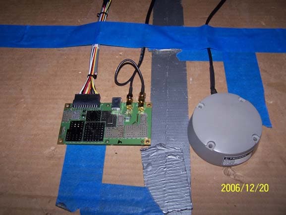
Click to zoom
Application Details
- Equipment Class
- TNB - Licensed Non-Broadcast Station Transmitter
- Date of Grant
- May 08, 2007
- Application Purpose
- Original Equipment
- Date of Application
- Jan 23, 2007
- Equipment Note
- Satellite Transmitter Module
- Frequency Range
- 1610.73000000 - 1620.57000000
- Company
- Qualcomm Technologies, Inc.
- Country
- United States
Documents & Files
Document Text
Text extracted from the exhibit documents filed with the FCC. Open a document above to read the original.
Users Manual
80-C6495-1 Rev. AQUALCOMM Confidential and Proprietary8-1 8 INTEGRATING GSP-1720 MODULES INTO PRODUCTS Integrators can buy QUALCOMM Globalstar GSP-1720 Satellite Data/Voice Modules in bulk direct from QUALCOMM to incorporate them into market-specific products. As an integrator, you provide custom module and antenna cables as appropriate to your specific products. You must also mount the module boards in protective enclosures, which field technicians can then install on-site, connected to antennas. This chapter is intended for: •Integrators who incorporate GSP-1720 hardware into products (for example, oil pipeline monitors) •Field technicians who install those products on site It is assumed that integrators and field technicians can work directly from the technical specifications. This chapter contains the following information: •Integrating modules into products THardware description of the module, including mechanical descriptions; specifications; Data and Control port signaling and pinouts; DC power; and grounding information TGuidelines for mounting modules in enclosures •Mounting antennas on-site TAntenna cable specifications and lengths Integrator’s Reference Manual 8-2QUALCOMM Confidential and Proprietary80-C6495-1 Rev. A TPositioning antennas for Globalstar service, and mounting and sealing antennas •Environmental specifications for the GSP-1720 and antenna Caution For your safety and to avoid potential damage to the equipment, observe the Cautions and Warnings on page xxiv. Caution When integrating the GSP-1720 and its antenna into products, be sure to abide by all RF restrictions as described in Appendix A. Integrating Modules into Products This section describes the QUALCOMM Globalstar GSP-1720 Satellite Data/Voice Module hardware, including mechanical descriptions of the module, its Data and Control port signals and pinouts, DC power, and grounding. Using this information for your specific products, you can create custom cables, which connect a module (the DCE) to: •A terminal or processor (the DTE) running custom application software for your product — using the Data port only, or both Data and Control ports •An appropriate DC power source •Antenna — for information about installing antennas and calculating cable lengths, see Mounting Antennas at the Field Site on page 8-17. Note The Diagnostic port uses a standard USB cable. Integrating GSP-1720 Modules into Products 80-C6495-1 Rev. AQUALCOMM Confidential and Proprietary8-3 Module Mechanical Description The GSP-1720 is a single circuit card assembly (CCA) that is open and unprotected. As a result, the GSP-1720 must be shielded from direct impacts, precipitation, and particulates. I/O is obtained through four connectors: •Power, Data, and Control functions are accessed via a 22-pin connector (labeled J4 on the board). •Globalstar RF transmit signals are routed to an SMA-style coaxial connector (labeled J2 on the board). •Globalstar RF receive signals are routed to an SMA-style coaxial connector (labeled J1 on the board). •The Diagnostic port uses a standard USB cable (labeled J3 on the board). Module Board Layout This section includes the following technical drawings depicting the module: •GSP-1720 Module Board Layout (Top View), Figure 8-1 •GSP-1720 Module Board Layout (Side and Bottom View), Figure 8-2 Note In Figure 8-1 and Figure 8-2, dimensions are shown as: millimeters [inches]. Millimeters are the controlling dimensions on these drawings. Inch dimensions are for reference only. Integrator’s Reference Manual 8-4QUALCOMM Confidential and Proprietary80-C6495-1 Rev. A Figure 8-1. GSP-1720 Module Board Layout (Top View) Integrating GSP-1720 Modules into Products 80-C6495-1 Rev. AQUALCOMM Confidential and Proprietary8-5 Figure 8-2. GSP-1720 Module Board Layout (Side/ Bottom Views) Integrator’s Reference Manual 8-6QUALCOMM Confidential and Proprietary80-C6495-1 Rev. A Module Dimensions and Weight Module dimensions are 119 x 65x 14 millimeters (4.69 x 2.56 x 0.55 inches). Module weight is less than 60 grams (2.15 ounces). Module Antenna Connectors The GSP-1720 has two (2) sma screw-on connectors for the antenna leads, connecting the antenna to the module: •Transmit (Tx) lead is labeled J2. •Receive (Rx) lead is labeled J1. Caution The SMA connectors are secured only by a solder joint and are not designed to withstand excessive force. When cables are connected to these connectors, care must be taken to ensure adequate strain relief is provided. Data and Control Ports The Data and Control ports are combined into a single 22-pin Molex serial connector, which provides the primary user interface: •The connector contains two (2) 9-pin serial ports, DC power leads, and a reset lead. •Line speed for the Data port is variable between 300 bps and 38400 bps. (This is different from the over-the-air effective throughput, which is 9600 bps.) •Line speed for the Control port is fixed at 9600 bps. •Signaling uses 8 bits, no parity and 1 stop bit (8,N,1). •All ports are ESD and short-circuit protected. Note The Data port can be set to either USB or serial. Refer to Chapter 5 for setting port configurations. Note The module signal naming convention assumes that the module is the DCE and that the user application is the DTE. Integrating GSP-1720 Modules into Products 80-C6495-1 Rev. AQUALCOMM Confidential and Proprietary8-7 Note Pin 13 in the 22-pin Molex connector is used for power on/off. Pull the pin low to power on the module. By floating or pulling the pin high (4.7 V), the module will power down. Control Port Signals The Control port (CP) is an RS-232-level asynchronous interface operating at 9600 bps using Transmit Data (TxD), Receive Data (RxD), Data Terminal Ready (DTR), Data Set Ready (DSR), and Signal Common (GND). RxD and TxD perform data transfer and handshaking, while DTR is used to turn on the module and to let it know that there is an application waiting to talk to it. The Control port specifically allows dedicated usage of the …
Text truncated - open the document above for the full version.
Attestation Statements
Page 1 Exhibit 3 Attestation Statement The equipment, QUALCOMM model Globalstar K2 User Terminal (UT), is a satellite communications user terminal designed to operate under the requirements of FCC CFR47 Part 25. The product is designed to operate at a granted level of 2.5 Watts E.I.R.P. (1.53 Watts ERP). The equipment complies with uncontrolled RF exposure environment requirement by the IEEE STD C95.1 and FCC OET Bulletin 65, Edition 97-01 August 1997. The data, data evaluation and equipment configuration represented herein for equipment certification are a true and accurate representation of the measurements of the sample’s radio frequency interference emissions characteristics as of the dates and at the times of the test under the conditions herein specified. This applies to all tests that do not require an Open Area Test Site (OATS) to perform. Nemko USA performed tests that required an OATS site. Equipment Tested: GSP-1720 Globalstar K2 SDVM Part 25 References: 25.202 Frequency Stability 25.202 Emissions Limits Part Number: 20-C6493-1 Serial Number: N10D6XC3X Dates of Test: November 15, 2006 to December19, 2006 Test Performed by: Paul Jayne Senior EMC/Regulatory Engineer Qualcomm Incorporated
Cover Letter(s)
QUALCOMM Incorporated 5775 Morehouse Drive San Diego, CA 92121-1714 www.qualcomm.com 02 January, 2007 Nemko Canada Inc 303 River Road Ottawa, Ontario, Canada K1V 1H2 Attn: Director of Certification Authority to Act as Agent On our behalf, I appoint Nemko USA, Inc. 11696 Sorrento Valley Rd., Suite F, San Diego, CA 92121, to act as our agent in the preparation of this application for equipment certification. I certify that submitted documents properly describe the device or system for which equipment certification is sought. I also certify that each unit manufactured, imported or marketed, as defined in Industry Canada’s regulations will have affixed to it a label identical to that submitted for approval with this application. For instances where our authorized agent signs the application for certification on our behalf, I acknowledge that all responsibility for complying with the terms and conditions for certification, as specified by Nemko Canada Inc, still resides with Qualcomm Inc., 5775 Morehouse Dr., San Diego, CA, 92121. Dated this 8th Day of January 20 07 Agency agreement expiration date: 08 January, 2008 By: Paul Jayne Signature Printed Title: Senior EMC Engineer On behalf of : Qualcomm Inc. telephone: 858-651-1758
Cover Letter(s)
QUALCOMM Incorporated 5775 Morehouse Drive San Diego, CA 92121-1714 www.qualcomm.com 19 January 2007 Pursuant to FCC rule part 25 section 25.129, which indicates that as a device that does not support an ancillary terrestrial component (ATC), the Globalstar Satellite Data/Voice Modem (SDVM) does not require certification under 25.149(c). Qualcomm has been notified by Nemko USA that this device does not require certification, and that Qualcomm is requesting that this device does receive certification since we are contractually obligated to obtain certification by our customers. Sincerely, Paul Jayne Senior EMC Engineer Qualcomm Incorporated 5775 Morehouse Dr. San Diego, CA 92121
Cover Letter(s)
QUALCOMM Incorporated 5775 Morehouse Drive San Diego, CA 92121-1714 www.qualcomm.com Applicant: Qualcomm Inc. FCC ID: J9CGSSDVM Exhibit 2 Cover Letters QUALCOMM Incorporated 5775 Morehouse Drive San Diego, CA 92121-1714 www.qualcomm.com 08 January 2007 Equipment Autorisation Division Federal Communications Commission 7435 Oakland Mills Road Columbia, MD 21046 FCC ID:__J9CGSSDVM__ __ Product Name:_GSP-1720_ Pursuant to Sections 0.457 and 0.459 of the commissions rules, we hereby request that the following documents be held confidential: Exhibit 6-Block Diagram Exhibit 10-Schematics Exhibit 11-Parts List These materials contain trade secrets and proprietary information and are not customarily released to the public. The public disclosure of this information might be harmful to the company and provide unjustified benefits to our competitors. Dated this 2nd Day of January 20 07 By: Paul Jayne Signature Printed Title: Senior EMC Engineer On behalf of : Qualcomm Inc. Telephone: 858-651-1758
External Photos
Applicant: Qualcomm Inc. FCC ID: J9CGSSDVM Exhibit 8 External Photos Top View Top View-Close Up PCB, Antenna & Cables PCB Close Up RF Exposure Label
ID Label/Location Info
Applicant: Qualcomm Inc. FCC ID: J9CGSSDVM Exhibit 5 FCC Identifier Label
Internal Photos
Applicant: Qualcomm Inc. FCC ID: J9CGSSDVM Exhibit 9 Internal Photos PCB With Shields In Place PCB Bottom View PCB Side View PCB With Shields Removed PCB Detail-Right Side PCB Detail-Left Side
Operational Description
Applicant: Qualcomm Inc. FCC ID: J9CGSSDVM Exhibit 4 Product Overview (Part 2.1033) 1.1 Technical Description The GSP-1720 Globalstar Satellite Data Voice Modem (SDVM) operates in Globalstar mode only, communicating directly with overhead Globalstar satellites and via those satellites to the nearest Globalstar Gateway and through the Gateway the rest of the network. The service supports voice and data communications and provides user position location information. The User Terminal uses Code Division Multiple Access (CDMA) technology to provide secure, dependable service to the user. 1.2 Address of Manufacturer and Applicant 2.1033 (c) (1) Manufacturer: Qualcomm Incorporated 5775 Morehouse Drive San Diego, CA 92121 Telephone: (858) 587-1121 Applicant: QUALCOMM, INC. 5775 Morehouse Dr. San Diego, CA 92121 Telephone: (858) 587-1121 1.3 FCC Identifier 2.1033 (c) (2) The FCC identifier is: J9CGSSDVM 1.4 User Manual 2.1033 (c) (3) See Error! Reference source not found.User Manual 1.5 Types of Emissions 2.1033 (c) (4) 1M25G1W 1.6 Frequency Range 2.1033 (c) (5) Each Globalstar SDVM is capable of transmitting on any one of the frequency channels defined between 1610 and 1626.5 MHz. In the US and other countries where one or more TDMA mobile satellite service (MSS) low earth orbit (LEO) systems are authorized to operate, Globalstar SDVMs transmit (and are authorized to transmit) in only the lower 9 of the 13 channels, operating in the frequency range from 1610 to 1621.35 MHz. Depending on local Globalstar traffic conditions, a given SDVM may be assigned to operate on any of the authorized channels for a given call. Multiple access and efficient frequency re-use is provided by means of code division multiple access (CDMA) technology 1.7 Operating Power Levels 2.1033 (c) (6) Active power control is employed in the Globalstar system to minimize collateral interference between proximate Globalstar subscribers, since as is true of any multiple access spread spectrum system, other users signals represent noise to a given users signal. Thus all signals are automatically reduced to minimum power levels by the system, transparently to the user. As defined in the Globalstar Air Interface (GAI) Specification (80-25118-1), the effective isotropic radiated power (EIRP) of a mobile UT operating at maximum power output is 2.5 Watts. 1.8 DC Supply and Current Range 2.1033 (c) (8) The UT is powered by an external DC power supply, which provides a nominal 5.0 VDC (4.7-5.1 VDC range) at 0.1 to 1.0 Amperes current draw, 5.1 Watts maximum load. Power to the transmitter power amplifier (PA) passes through multiple switching and analog power regulator stages, and the PA is not affected by any changes in the supply voltage. It is thus immune to any effects of voltage fluctuation within the defined DC power voltage input range of the UT. Outside that range the UT simply shuts down. 1.9 List of Semiconductor Active Devices 2.1033 (c) (10) See Exhibit 11-Parts List. 1.10 Circuit Diagram 2.1033 (c) (10) See Exhibit 10-Schematics. 1.11 Transmitter Adjustment Procedure 2.1033 (c) (9) All frequency adjustments are set at the factory and there are no frequency field adjustments for this product. The transmit frequency is locked to the base station and controlled by VCTCXO adjustments to offset any possible errors. 1.12 Frequency Stability Device 2.1033 (c) (10) All RF oscillators are phase-lock loop locked to the output signal of a voltage controlled temperature compensated crystal oscillator (TCXO), the master oscillator of the system. It is specified to provide frequency accuracy to better than 10 parts per million over the UT’s 5 year design life, with +/-5 ppm allocated to TCXO aging. Exhibit 13 details the temperature variation frequency stability test results which have been obtained. Due to the relatively large Doppler error inherent to an LEO communications system, transmit frequencies are locked to the TCXO signal and are not adjusted based on frequency differences with respect to Gateway transmitted signals. 1.13 Spurious Radiation Suppression Devices 2.1033 (c) (10) See Exhibit 14 and Exhibit 15 1.14 Drawing of Equipment Identification Plate or Label 2.1033 (c) (11) See Exhibit 5-Label. 1.15 Photographs 2.1033 (c) (12) See Exhibit 6 and Exhibit 11 1.16 Modulation Technique 2.1033 (c) (13) The Globalstar Air Interface uses a modified form of IS-95 to support Code Division Multiple Access. CDMA was selected for Globalstar because it represents a proven technology that can provide efficient modulation scheme for satellite communications. It is relatively interference tolerant, both from a standpoint of generation of interference to other services and tolerating outside interference. As a bonus, there is a level of security inherent in the modulation scheme. It is difficult to listen into conversations or to pirate services from the system. CDMA is able to provide good voice quality while operating at relatively low RF power levels. The Globalstar CDMA is based on the existing QUALCOMM CDMA product line used for terrestrial cellular communications. 1.17 Test Data 2.1033 (3) (14) See exhibit 14, 15 & 16. 1.18 RF Block Diagram See exhibit 6 block diagram
Parts List/Tune Up Info
Applicant: Qualcomm Inc. FCC ID: J9CGSSDVM Exhibit 17 Tune-Up Procedure The QUALCOMM Globalstar Satellite Data/Voice Modem (SDVM) is designed using a phase loop-locked (PLL) RF subsection. As a result of this design, there is no end-user or field service tune up procedure for this product. All frequency adjustments are made in the factory prior to shipment and no other tuning is necessary. Paul Jayne Senior EMC Engineer Qualcomm Incorporated 5775 Morehouse Dr. San Diego, CA 92121
RF Exposure Info
Prediction of MPE limit at a given distance Equation from page 18 of OET Bulletin 65, Edition 97-01where: S = power density P = power input to the antennaG = power gain of the antenna in the direction of interest relative to an isotropic radi a R = distance to the center of radiation of the antenna Maximum peak output power at antenna input terminal: 29.50 (dBm) Maximum peak output power at antenna input terminal: 891.2509381 (mW) Antenna gain(typical): 4.5 (dBi) Maximum antenna gain: 2.818382931 (numeric) Prediction distance: 25 (cm) Prediction frequency: 1615 (MHz) MPE limit for uncontrolled exposure at prediction frequency: 1.000 (mW/cm^2) Power density at prediction frequency: 0.319823 (mW/cm^2) Maximum allowable antenna gain: 9.450898814 (dBi) Margin of Compliance: 4.950898814 2 4 R PG S π =
Test Report
Applicant: Qualcomm Inc. FCC ID: J9CGSSDVM Exhibit 13 Frequency Stability Exhibit 13- Transmitter Carrier Frequency Stability- FCC Part 2.1055 Transmitter RF Carrier Frequency Stability- FCC Part 2, Paragraph 2.1055 Measured with an Anritsu MT8803 Globalstar User Terminal Tester The SDVM was tested at the extreme high and low voltages at which the unit will operate without shutting down. Therefore, it was not possible to test the unit for frequency stability at +/- 15% the nominal voltage. The listed operating voltage range for the SDVM is 4.9-5.1 VDC. 4.7V4.9V5.3V temp CHz offsetHz offsetHz offsetlower limitupper limit -30-433-365-433-40254025 -20-628-286-405-40254025 -10-499-369-377-40254025 0-258-667-457-40254025 10-376-461-474-40254025 20-471-766-348-40254025 25-309-473-425-40254025 30-167-264-316-40254025 40-388-460-472-40254025 50-675-573-438-40254025 60-598-619-507-40254025 4.7V4.9V5.3V temp CHz offsetHz offsetHz offsetlower limitupper limit -30-377-907-905-40604060 -20-451-953-877-40604060 -10-538-1003-949-40604060 0-453-983-879-40604060 10-670-805-852-40604060 20-622-571-778-40604060 25-589-429-673-40604060 30-476-91-534-40604060 40-325-44-486-40604060 50-265-442-370-40604060 60-488-598-548-40604060 Specification Variation from carrier frequency reference (Hz)-Channel 1 Variation from carrier frequency reference (Hz)-Channel 9 Specification Channel 1 Frequency Stability -5000 -4000 -3000 -2000 -1000 0 1000 2000 3000 4000 5000 -30-20-10010202530405060 temp (degrees C) variation from carrier frequency reference (Hz) Lower Limit Upper Limit 4.7V 4.9V 5.3V Channel 9 Frequency Stability -5000 -4000 -3000 -2000 -1000 0 1000 2000 3000 4000 5000 -30-20-10010202530405060 temp (degrees C) variation from carrier reference (Hz) 4.7V 4.9V 5.3V Lower Limit Upper Limit
Test Report
Globalstar K2 SDVM GSP-1720 FCC Part 25 Type Acceptance Report with Exhibits Conducted Me Applicant: QUALCOMM Incorporated FCC ID: J9CGSK2UT Exhibit 15 Conducted Test Data 1.1 Compliance Lab Test Equipment The following table is a list of equipment used in the compliance lab during the testing of the GSP-1700. Model NumberManufacturerSerial NumberDescriptionCalibration Date Calibration Due Date 8542CGigatronicsK82262Power Meter7/26/20067/26/2007 8542CGigatronicsK64822Power Meter2/1/20062/1/2007 80401AGigatronicsK69842Power Sensor8/28/20068/28/2007 80401AGigatronicsX21061Power Sensor7/22/20067/22/2007 6632BHewlett PackardX100188Power Supply7/27/20067/27/2007 6647AHewlett PackardK60687Power Supply4/4/20064/4/2007 2031Marconi InstrumentsK64729Signal Generator4/3/20064/3/2007 FSEM20Rohde & SchwarzX06071Spectrum Analyzer4/21/20064/21/2007 MT8803GAnritsuX05786Globalstar UT Tester12/22/200512/22/2006 1.2 Receiver Type The Globalstar K2 SDVM receiver is a standard Sperheterodyne design. 1.3 Compliance Lab Conducted Data The Globalstar transmit channel carrier frequency is found by the formula: Fc(MHz)= 1610.64 + 0.03(N-1) Where Fc is the carrier frequency and N is a fractional channel multiplier in the range of 4≤N≤509 The compliance lab test data is listed by the channel number N value which correspond to the following Globalstar channels and frequencies: Globalstar Channel Number N= Frequency (MHz) 1 4 1610.73 6 250 1616.88 9 332 1620.57 dBW to dBW EIRP Conversion in the frequency band 1559-1610 MHz In order to convert the units from dBW to dBW EIRP for the frequency range 1559-1610 MHz, the peak antenna gain has been added to the conducted power level. The antenna gain has been added as a correction factor in the reverse link test station and is automatically added to the raw data resulting in the trace plots for these frequency ranges. Globalstar K2 SDVM GSP-1720 FCC Part 25 Type Acceptance Report with Exhibits Conducted Me Applicant: QUALCOMM Incorporated FCC ID: J9CGSK2UT Tx Max Power Channel 1 Tx Max Power Channel 7 Globalstar K2 SDVM GSP-1720 FCC Part 25 Type Acceptance Report with Exhibits Conducted Me Applicant: QUALCOMM Incorporated FCC ID: J9CGSK2UT Tx Max Power Channel 9 Out of Band Emissions Globalstar K2 SDVM GSP-1720 FCC Part 25 Type Acceptance Report with Exhibits Conducted Me Applicant: QUALCOMM Incorporated FCC ID: J9CGSK2UT Globalstar K2 SDVM GSP-1720 FCC Part 25 Type Acceptance Report with Exhibits Conducted Me Applicant: QUALCOMM Incorporated FCC ID: J9CGSK2UT Occupied Bandwidth Channel 1 Channel 7 Globalstar K2 SDVM GSP-1720 FCC Part 25 Type Acceptance Report with Exhibits Conducted Me Applicant: QUALCOMM Incorporated FCC ID: J9CGSK2UT Channel 9 1605-1610 Spurious Emissions Channel 1 Globalstar K2 SDVM GSP-1720 FCC Part 25 Type Acceptance Report with Exhibits Conducted Me Applicant: QUALCOMM Incorporated FCC ID: J9CGSK2UT Channel 7 Channel 9 Globalstar K2 SDVM GSP-1720 FCC Part 25 Type Acceptance Report with Exhibits Conducted Me Applicant: QUALCOMM Incorporated FCC ID: J9CGSK2UT 1605-1610 narrowband spurious emissions Channel 1 Channel 7 Globalstar K2 SDVM GSP-1720 FCC Part 25 Type Acceptance Report with Exhibits Conducted Me Applicant: QUALCOMM Incorporated FCC ID: J9CGSK2UT Channel 9 Receive Band Mean Power Emissions Globalstar K2 SDVM GSP-1720 FCC Part 25 Type Acceptance Report with Exhibits Conducted Me Applicant: QUALCOMM Incorporated FCC ID: J9CGSK2UT Standby Output Power Emission Mask Channel 1 Globalstar K2 SDVM GSP-1720 FCC Part 25 Type Acceptance Report with Exhibits Conducted Me Applicant: QUALCOMM Incorporated FCC ID: J9CGSK2UT Emission Mask Channel 9 1559-1610 MHz Carrier Off Compliance Lab Data SummaryTime Test Name Test # Test Description Fwd Chnl Rev Chnl Low Actual High Units Status Temp Volts UT for MES used on the Globalstar System GSP1720 SDV M 12/18/2006 6:44:01 PM Equipment Identity ETSI TBR 041 p10 Anritsu=310005000000000 UTDM=310005000000000 63 4 0 0 0 MSID 25.00 5.10 V *C 12/18/2006 6:44:01 PM Equipment Identity ETSI TBR 041 p10 Anritsu=741196BB UTDM=741196BB 63 4 0 0 0 ESN 25.00 5.10 V *C 12/20/2006 3:45:49 PM ETSI Unwanted RX EmissionsPlot# 1148 MPS 2.6.1.3.1 Plot Reference10.00 to 30.00 MHz 63 4 0 0 0 25.00 5.10 V *C 12/20/2006 3:46:01 PM ETSI Unwanted RX EmissionsPlot# 1149 MPS 2.6.1.3.1 Plot Reference30.00 to 1000.00 MHz 63 4 0 0 0 25.00 5.10 V *C 12/20/2006 3:46:09 PM ETSI Unwanted RX EmissionsPlot# 1150 MPS 2.6.1.3.1 Plot Reference1000.00 to 3000.00 MHz 63 4 0 0 0 25.00 5.10 V *C 12/20/2006 4:24:35 PM ETSI Unwanted RX EmissionsPlot# 1455 MPS 2.6.1.3.1 Plot Reference10.00 to 30.00 MHz 63 250 0 0 0 25.00 5.10 V *C 12/20/2006 4:24:46 PM ETSI Unwanted RX EmissionsPlot# 1456 MPS 2.6.1.3.1 Plot Reference30.00 to 1000.00 MHz 63 250 0 0 0 25.00 5.10 V *C 12/20/2006 4:24:54 PM ETSI Unwanted RX EmissionsPlot# 1457 MPS 2.6.1.3.1 Plot Reference1000.00 to 3000.00 MHz 63 250 0 0 0 25.00 5.10 V *C 12/20/2006 4:47:25 PM ETSI Unwanted RX EmissionsPlot# 1637 MPS 2.6.1.3.1 Plot Reference10.00 to 30.00 MHz 63 332 0 0 0 25.00 5.10 V *C 12/20/2006 4:47:36 PM ETSI Unwanted RX EmissionsPlot# 1638 MPS 2.6.1.3.1 Plot Reference30.00 to 1000.00 MHz 63 332 0 0 0 25.00 5.10 V *C 12/20/2006 4:47:44 PM ETSI Unwanted RX EmissionsPlot# 1639 MPS 2.6.1.3.1 Plot Reference1000.00 to 3000.00 MHz 63 332 0 0 0 25.00 5.10 V *C 12/20/2006 3:46:57 PM FCC Unwanted RX EmissionsPlot# 1151 MPS 2.6.1.3.3 Plot Reference1.00 to 10.00 MHz 63 4 0 0 0 25.00 5.10 V *C 12/20/2006 3:47:02 PM FCC Unwanted RX EmissionsPlot# 1152 MPS 2.6.1.3.3 Plot Reference10.00 to 30.00 MHz 63 4 0 0 0 25.00 5.10 V *C 12/20/2006 3:47:10 PM FCC Unwanted RX EmissionsPlot# 1153 MPS 2.6.1.3.3 Plot Reference30.00 to 1000.00 MHz 63 4 0 0 0 25.00 5.10 V *C Page 1 N10D6XBHK P2 R7.1.1.2.2 Software: Hardware Serial #: 4:18:13 PM Tuesday, January 02, 2007 SDVM QUALCOMM Proprietary Time Test Name Test # Test Description Fwd Chnl Rev Chnl Low Actual High Units Status Temp Volts UT f or MES used on the Globalstar S y stem GSP172…
Text truncated - open the document above for the full version.
Test Report
Applicant: Qualcomm Inc. FCC ID: J9CGSSDVM Exhibit 16 Conducted Measurement Test Procedure Globalstar Compliance Lab Reverse Link Test Procedures 80-98735-1 X1 Export of this technology may be controlled by the United States Government. Diversion contrary to U.S. law prohibited. QUALCOMM is a registered trademark and registered service mark of QUALCOMM Incorporated. Other product and brand names may be trademarks or registered trademarks of their respective owners. Copyright © 2006 QUALCOMM Incorporated. All rights reserved. Globalstar Compliance Lab Reverse Link Test Procedures 80-98735-1 X1 January 9, 2007 Globalstar Compliance Lab Reverse Link Test Procedures Tables 80-98735-1 X1 QUALCOMM Proprietary iii Table of Contents 1. Introduction ....................................................................................................... 1-1 1.1 Scope of this Document ................................................................................ 1-1 1.2 List of Abbreviations/Acronyms ...................................................................1-1 2. Applicable Documents ..................................................................................... 2-1 2.1 Document Requirements .............................................................................. 2-1 3. Requirements .................................................................................................... 3-1 3.1 General .......................................................................................................... 3-1 4. Procedures ........................................................................................................ 4-1 4.1 General .......................................................................................................... 4-1 4.1.1 Measurement Notes ................................................................................ 4-1 4.1.2 Calibration............................................................................................... 4-1 4.1.3 Test Sequences........................................................................................ 4-1 4.2 Access Probe Power Time Response ............................................................ 4-1 4.2.1 Definition................................................................................................. 4-1 4.2.2 Reference ................................................................................................. 4-2 4.2.3 Setup........................................................................................................ 4-2 4.2.4 Measurement Method............................................................................. 4-3 4.2.5 Criteria .................................................................................................... 4-5 4.2.6 Test Report .............................................................................................. 4-5 4.3 Access Channel Waveform Quality, Timing, and Frequency Accuracy ..... 4-5 4.3.1 Definition................................................................................................. 4-5 4.3.2 Reference ................................................................................................. 4-6 4.3.3 Setup........................................................................................................ 4-6 4.3.4 Measurement Method............................................................................. 4-6 4.3.5 Criteria: ................................................................................................... 4-6 4.3.6 Test Report .............................................................................................. 4-6 4.4 Minimum Controlled Output Power ............................................................ 4-7 4.4.1 Definition................................................................................................. 4-7 4.4.2 Reference ................................................................................................. 4-7 4.4.3 Setup........................................................................................................ 4-7 4.4.4 Measurement Method............................................................................. 4-7 Introduction Globalstar Compliance Lab Reverse Link Test Procedures iv QUALCOMM Proprietary 80-98735-1 X1 4.4.5 Criteria.....................................................................................................4-8 4.4.6 Test Report ..............................................................................................4-8 4.5 Access Probe Output Power and Standby Output Power............................4-8 4.5.1 Definition .................................................................................................4-8 4.5.2 Reference..................................................................................................4-8 4.5.3 Setup ........................................................................................................4-8 4.5.4 Measurement Method......................................................................…
Text truncated - open the document above for the full version.
Contact Information
Applicant
Paul Guckian(Vice President, Regulatory Engineering)
Technical Contact
Qualcomm IncorporatedPaul Jayne
[email protected]858-651-1758
5775 Morehouse Drive · San Diego, California · United States
Non-Technical Contact
Qualcomm IncorporatedPaul Jayne
[email protected]858-651-1758
Test Firm
Nemko USA, Inc.Rhonda Saxon
Technical Specifications
| # | Rule Parts | Frequency Range | Power Output | Emission | Tolerance |
|---|---|---|---|---|---|
| 1 | 25 | 1.61 GHz - 1.62 GHz | 2.5 W | 1M25G1W | 5.0000000000 ppm |
Other Applications from Qualcomm Technologies, Inc.
J9C-M2X75
Aug 13, 2024Module
Equipment Class
CBE - Citizens Band End User DevicesJ9C-M2X72
Aug 13, 2024Module
Equipment Class
PCB - PCS Licensed Transmitter
J9C-QCNCM825
Aug 26, 2023Qualcomm WiFi 7/BT Combo module
Equipment Class
6CD - 15E 6 GHz Low Power Dual Client
J9C-QCNCM865
Apr 04, 2023Qualcomm WiFi 7/BT Combo module
Equipment Class
NII - Unlicensed National Information Infrastructure TX
J9CQCARD7280N
Nov 07, 2022QCARD7280
Equipment Class
DTS - Digital Transmission System