JOFRS9803UDAIntegrated Motorcycle 40 Channel AM CB Transceiver
Radio Sound Inc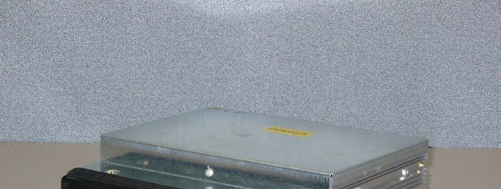
Click to zoom
Application Details
- Equipment Class
- TNB - Licensed Non-Broadcast Station Transmitter
- Date of Grant
- Feb 02, 2004
- Application Purpose
- Original Equipment
- Date of Application
- Feb 02, 2004
- Equipment Note
- Integrated Motorcycle 40 Channel AM CB Transceiver
- Frequency Range
- 26.96500000 - 27.40500000
- Company
- Radio Sound Inc
- Country
- United States
Documents & Files
Document Text
Text extracted from the exhibit documents filed with the FCC. Open a document above to read the original.
Users Manual
Citizen’s Band Radio Transceiver Operating Instructions (Excerpted From Main overall Motorcycle Instruction Manual)
External Photos
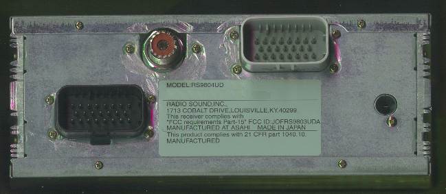
Figure 1 – Front Side Figure 2 - Back
Internal Photos
Figure 1 – Top Cover Removed Figure 2 – Bottom Cover Removed Figure 3 – CD Player Removed Figure 4 – Bottom PCB Exposed Figure 5 – Bottom PCB (Top) Figure 6 – Bottom PCB (Bottom)
Internal Photos
Figure 1 – Top PCB (Top) Figure 8 – Top PCB (Bottom) Figure 9 – Bottom PCB Shield Removed (Bottom)
Parts List/Tune Up Info
7. Tune Up Procedure Description: Receiver Alignment Procedure: a. Connect the transceiver to the test box console. Insure that the applied DC voltage is 14.0 Volts (+/- 0.2 volts). Do not turn on the transceiver yet. b. Attach the output of the RF signal generator to the transceiver antenna input jack. Set the signal generator output to 27.205 MHz, 1.0 KHz AM modulation at 30%. Set the RF generator initial output level to 1.0 millivolt. Do not enable the generator RF output yet. c. Connect an audio power meter to the audio output of the transceiver through the test box console. d. Turn on the transceiver. Set the transceiver to Channel 20 (27.2050 MHz). Measure the VCO tuning voltage at the junction between R511 and R522 Carefully adjust VCO tank coil L4 until this voltage is 2.250 volts (+0.00, -0.05 volt). e. Verify that the receiver VCO frequency is correct and locked by connecting a frequency counter to pin 13 of IC3 PLL. The receiver VCO frequency should be 16.505 MHz. f. While observing the VCO frequency on pin 13 of IC3, change the transceiver to Channel 40. Verify that the frequency quickly changes and locks on 16.705 MHz. Measure the VCO voltage again at the junction between R511 and R522. This voltage should be approximately 3.50 volts, +/- 0.1 volt. g. While observing the VCO frequency on pin 13 of IC3, change the transceiver to Channel 1. Verify that the frequency quickly changes and locks on 16.265 MHz. Measure the VCO voltage again at the junction between R511 and R522. This voltage should be approximately 1.40 volts, +/- 0.1 volt. The VCO is now properly adjusted. h. Set the transceiver to Channel 20 (27.205 MHz). Enable the RF generator (level = 1.0 mV) as set up in Step b above. Adjust the following coils in the order listed for peak audio output on the power meter: L5: First RF Amp Output Filter L7: First Mixer Input Filter L9: First Mixer (10.7 MHz) Tank Circuit L16: Second Mixer (455 KHz) Tank Circuit L17: AM Detector (455 KHz) Tank L1: Antenna Input Matching (tunes very broadly) L11: LO Output Filter Reduce the signal generator RF level to 1.0 microvolt. Re-peak all of the coils listed above in the same order for maximum output on the audio power meter. i. With the RF signal generator set to 1.0 microvolt and 30% AM modulated with the 1.0 KHz tone and all coils peaked, set the audio power meter needle position to the 0 dB level by adjusting the transceiver output volume or rotating the power meter “relative adjust” control. Remove the 1 KHz modulation signal from the RF signal generator carrier and measure the resulting change in audio power. Verify that the drop in audio power is 10 dB or greater. This completes the receiver alignment procedure. Transmitter Frequency Lock and Maximum Output Power Alignment: a. Connect the radio to the test/control interface box. Apply nominal +14 VDC (+/- 0.2 volt) through the radio rear panel connector. b. Connect the antenna output jack to the 30 dB attenuator/50 ohm load and the attenuator output to the combination power level, frequency and modulation measurement meter. c. Turn on the radio and select CB mode with the control box switch. Set the transceiver to Channel 40 (27.405 MHz). d. Measure the Transmitter VCO DC voltage from the PLL at the junction between R511 and R522. Verify that this voltage is 3.5 volts +/- 0.2 VDC. e. Measure the RX operating frequency at pin 13 of PLL IC 3 with a high input impedance frequency counter. Verify that the VCO is locked and oscillating at 16.705 MHz. Measure the active low lock detect signal on pin 5 of IC 3. This voltage should be more than 4.5 VDC to indicate PLL lock. Note: The TX VCO automatically shifts to ½ of the actual carrier output frequency on every channel (e.g. when on Channel 40, it shifts to 13.702.5 MHz) when PTT is pressed. Verify this shift by briefly pressing PTT while monitoring the PLL frequency on pin 13 of IC3. f. Set the transceiver to Channel 1 (26.965 MHz). Measure the Transmitter VCO DC voltage from the PLL at the junction between R511 and R522 when PTT is pressed. Verify that this voltage is 1.40 volts +/- 0.2 VDC. g. Set the transceiver to Channel 20 (27.205 MHz). Briefly press and release the PTT switch while observing the transmitted carrier frequency. If necessary, quickly adjust PLL crystal trimmer capacitor C45 for a precise frequency of 27.2050 MHz. h. Insure that the TX B+ voltage is set to 12.0 VDC (–0.0, +0.2 VDC) when measured at the collector of Q703. Adjust VR901 if necessary to obtain 12.0 volts at the collector of Q703. i. Engage the PTT switch. While transmitting, QUICKLY adjust the following coils for maximum observed power (output peaking) in the order listed while observing the transmitted power output: L601: Frequency Doubler Collector Tank L603: Frequency Doubler Output Tank L605: Frequency Doubler Output Buffer Tank L703: RF Pre-Amplifier Output L707: RF Power Amplifier Output L709: Carrier Frequency Second Harmonic Filter L711: Carrier Frequency Second Harmonic Filter j. If necessary, rotate the TX B+ control potentiometer VR901 counterclockwise (CCW) to reduce the transmitted carrier power to approximately 3.85 watts. Disengage the PTT switch. Change the transceiver to Channel 1. Press the PTT switch and observe the transmitted carrier power. Change the transceiver to Channel 40. Press the PTT switch and observe the transmitted carrier power. If the power on either Channel 1 or 40 is above 4.0 watts then reset the transceiver to whichever Channel (1 or 40) had the highest power and press PTT. Adjust VR901 CCW slightly until the maximum transmitted power on any channel is no greater than 3.90 watts. Release the PTT switch. k. Inject a 1 kHz, 3.3 volt peak-peak (1.17 volts RMS) signal into the “front” microphone input port on the console test box. Return the transceiver to Channel 20. Press the PTT switch while observing the modulation percentage on the modulation meter. Adjust modulation level potentiometer VR801 for a 90% (– 0/+5%) mod…
Text truncated - open the document above for the full version.
Test Report
This report may be reproduced only with the written permission of Intertek and if reproduced must be reproduced in its entirety. This report must not be used to claim product endorsement by NVLAP or any agency of the U.S. Government. The results contained in this report were derived from measurements performed on the identified test samples. Any implied performance of other samples based on this report is dependent on the representative adequacy of the samples tested. TEST REPORT Report Number: 3053114-001 Project Number: 3053114 1/20/2004 Evaluation of the US Domestic 40 Channel Citizen’s Band Transceiver Model Number: RS9804UDA FCC ID: JOFRS9803UDA FCC Part 2 FCC Part 15 FCC Part 95 Subpart E For Radio Sound Test Performed by: Test Authorized by: Intertek 731 Enterprise Drive Lexington, KY 40510 Radio Sound 1713 Cobalt Drive Louisville, KY 40299 Prepared By:_______________________________Date:____1/20/2004________ Bryan C. Taylor, EMC Team Leader Approved By:______________________________Date:____1/20/2004_________ David J. Schramm, EMC Team Leader Intertek 731 Enterprise Drive, Lexington, KY 40510 Telephone: 859-226-1000 Fax: 859-226-1040 Web: www.etlsemko.com 731 Enterprise Drive, Lexington KY 40510 Evaluation For:Radio Sound FCC ID: JOFRS9803UDA Model No: RS9804UDA File: 3053114 Page 2 of 45 FCC Part 2, 15, and 95 Evaluation TABLE OF CONTENTS 1 EXECUTIVE SUMMARY.......................................................................................................4 2 JOB DESCRIPTION................................................................................................................5 2.1 CLIENT INFORMATION............................................................................................................5 2.2 TEST PLAN REFERENCE:.........................................................................................................5 2.3 EQUIPMENT UNDER TEST (EUT)............................................................................................6 2.3.1 System Support Equipment.............................................................................................7 2.3.2 Cables associated with EUT...........................................................................................7 2.3.3 Justification..................................................................................................................8 2.3.4 Mode(s) of operation.....................................................................................................8 2.4 MODIFICATIONS REQUIRED FOR COMPLIANCE.........................................................................8 2.5 RELATED SUBMITTAL(S) GRANTS..........................................................................................8 3 TEST FACILITY.....................................................................................................................9 3.1 TEST EQUIPMENT................................................................................................................10 4 RF POWER OUTPUT............................................................................................................11 4.1 TEST PROCEDURE................................................................................................................11 4.2 BLOCK DIAGRAM................................................................................................................11 4.3 TEST RESULTS.....................................................................................................................11 5 MODULATION CHARACTERISTICS.................................................................................12 5.1 TEST PROCEDURE................................................................................................................12 5.2 BLOCK DIAGRAM................................................................................................................12 5.3 TEST RESULTS.....................................................................................................................13 6 OCCUPIED BANDWIDTH...................................................................................................17 6.1 TEST PROCEDURE................................................................................................................17 6.2 BLOCK DIAGRAM................................................................................................................17 6.3 TEST RESULTS.....................................................................................................................17 7 SPURIOUS EMISSIONS AT ANTENNA TERMINALS.......................................................23 7.1 TEST PROCEDURE................................................................................................................23 7.2 BLOCK DIAGRAM................................................................................................................23 7.3 TEST RESULTS.....................................................................................................................24 8 FIELD STRENGTH OF SPURIOUS RADIATION...............................................................30 8.1 TEST PROCEDURE................................................................................................................30 731 Enterprise Drive, Lexington KY 40510 Evaluation For:Radio Sound FCC ID: JOFRS9803UDA Model No: RS9804UDA File: 3053114 Page 3 of 45 FCC Part 2, 15, and 95 Evaluation 8.2 BLOCK DIAGRAM................................................................................................................30 8.3 TEST RESULTS.....................................................................................................................31 9 FREQUENCY STABILITY...................................................................................................37 9.1 TEST PROCEDURE.......................................................................................…
Text truncated - open the document above for the full version.
Test Setup Photos
Figure 1 – Output Power, Occupied Bandwidth, and Conducted Spurious Emissions Figure 2 – %Modulation vs. Frequency and Voltage Figure 3 – Frequency Stability vs. Temperature Figure 4 – Radiated Emissions Figure 5 – Radiated Emissions Figure 6 – Radiated Emissions
Contact Information
Applicant
Donald Tilley
Technical Contact
Radio sound IncDonald R Tilley
[email protected](502)267-6768
Radio Sound Inc · Louisville, Kentucky · United States
Non-Technical Contact
Radio sound IncDonald R Tilley
[email protected](502)267-6768
Test Firm
Intertek Testing ServicesJerry Marchal
606-226-1060
Technical Specifications
| # | Rule Parts | Frequency Range | Power Output | Emission | Tolerance |
|---|---|---|---|---|---|
| 1 | 95D | 26.965 MHz - 27.405 MHz | 4 W | A3E | 0.0050000000 % |
Other Applications from Radio Sound Inc
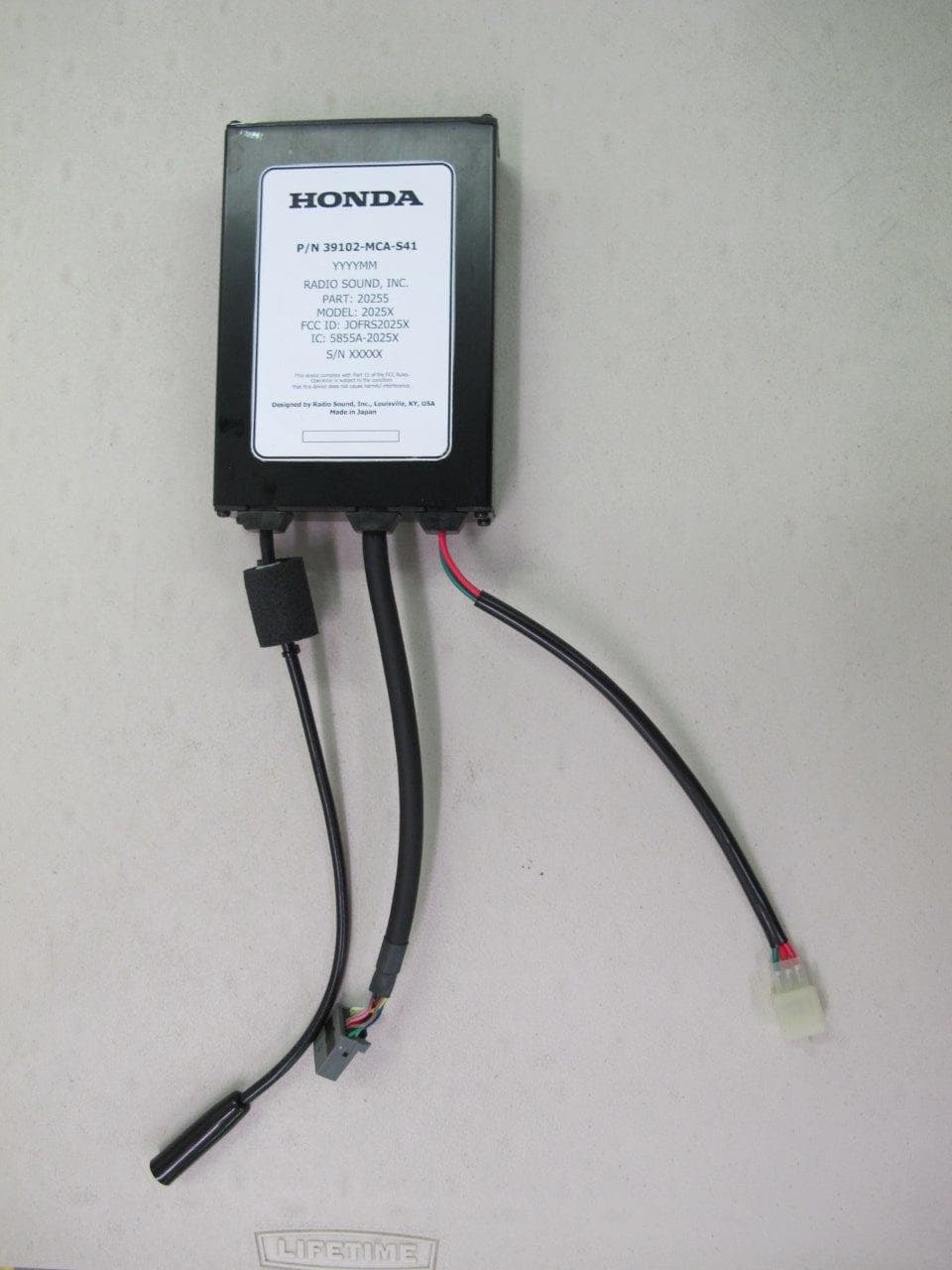
JOFRS2025X
Jul 24, 2014CB radio transceiver module
Equipment Class
TNB - Licensed Non-Broadcast Station Transmitter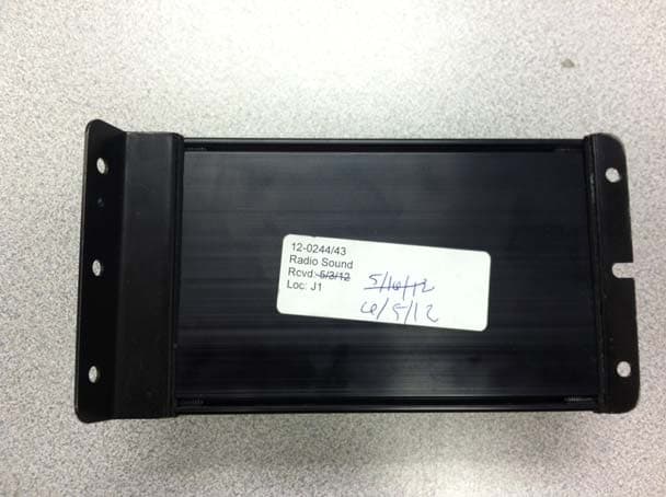
JOFRS51033
Aug 28, 2012CB RADIO TRANSCEIVER
Equipment Class
TNB - Licensed Non-Broadcast Station Transmitter
JOFRS20250
Mar 17, 2008Radio Sound Model RS20250
Equipment Class
TNB - Licensed Non-Broadcast Station Transmitter
JOFGMSH
Jun 28, 2005N-TOUCH GMRS Communication System
Equipment Class
FRB - Part 95 Family Radio Base Transmitter
JOFGMOR
Jun 28, 2005Arctic Cat N-Touch Communication System
Equipment Class
FRB - Part 95 Family Radio Base Transmitter