K7GR1050Two Way Radio with FRS and GMRS
Giant Electronics Ltd
Click to zoom
Application Details
- Equipment Class
- FRF - Part 95 Family Radio Face Held Transmitter
- Date of Grant
- Nov 30, 2005
- Application Purpose
- Original Equipment
- Date of Application
- Nov 30, 2005
- Equipment Note
- Two Way Radio with FRS and GMRS
- Frequency Range
- 467.56250000 - 467.71250000
- Company
- Giant Electronics Ltd
- Country
- Hong Kong
Documents & Files
Document Text
Text extracted from the exhibit documents filed with the FCC. Open a document above to read the original.
Users Manual
SAFETY AND GENERAL INFORMATION Important Information for Safe and Efficient Operation Please read this information before using your radio. Transmit and Receive Procedure Your two-way radio contains a transmitter and a receiver. To control your exposure and ensure compliance with the general population/uncontrolled environment exposure limits, do not transmit more than 50% of the time. Transmitting a maximum of 50% of the time, is important as the radio generates measurable RF energy exposure only when transmitting (in terms of measuring standards compliance). Antenna Care Do not try to modify the antenna. Unauthorized antennas, modifications, or attachments could damage the radio and may violate FCC regulations. Two-way Radio Operation When using your radio as a traditional two-way radio, hold the radio in a vertical position with the mircrophone 1 to 2 inches (2.5 to 5 cm) away from the lips. Body-Worn Operation To maintain compliance with FCC/Health Canada RF exposure guidelines, if you wear a radio on your body when transmitting, always place the radio in an approved clip, holder, holster, case, or body harness for this product. Use of non-approved accessories may exceed FCC/Health Canada RF exposure guidelines. Keep at least 1 inch (2.5 cm) from your body when transmitting if you do not use one of the supplied or approved body-worn accessories. Approved Accessories For a list of approved RCA accessories, visit our Web site at www.RCA.com. OPERATIONAL CAUTIONS Batteries All batteries can cause property damage and/or bodily injury such as burns if a conductive material—like jewelry, keys or beaded chains—touch exposed terminals. The conductive material may complete an electrical circuit (short circuit) and become quite hot. Exercise care in handling any charged battery, particularly when placing it inside a pocket, purse or other container with metal objects. FCC LICENSING INFORMATION Your radio operates on General Mobile Radio Service (GMRS) frequencies and is subject to the Rules and Regulations of the Federal Communications Commission (FCC). The FCC requires that all operators using GMRS frequencies obtain a radio license before operating their equipment. To obtain the FCC forms, please request Form 605 and 159, which includes all forms and instructions. If you wish to have the document faxed or mailed, or if you have questions, please use the following contact information: For a Fax: Contact the Fax-On- Demand system For Mail Service: Call the FCC Forms Hotline If You Have Questions about the FCC License: Call the FCC 1-202-418-0177 1-800-418-FORM (3676) 1-888-CALL-FCC (225-5322) You may also visit the FCC’s Web site at http://www.fcc.gov. Changes or modifications not expressly approved may void the user’s authority granted by the FCC to operate this radio and should not be made. To comply with FCC requirements, transmitter adjustments should be made only by or under the supervision of a person certified as technically qualified to perform transmitter maintenance and repairs in the private land mobile and fixed services as certified by an organization representative of the user of those services. Replacement of any transmitter component (crystal, semiconductor, etc.) not authorized by the FCC equipment authorization for this radio could violate FCC rules. Note: Use of this radio outside the country where it was intended to be distributed is subject to government regulations and may be prohibited. FCC STATEMENTS: This device complies with Part 15 of the FCC Rules. Operation is subject to the following two conditions: (1) this device may not cause harmful interference, and (2) this device must accept any interference received, including interference that may cause undesired operation. NOTE: This equipment has been tested and found to comply with the limits for a Class B digital device, pursuant to Part 15 of the FCC Rules. These limits are designed to provide reasonable protection against harmful interference in a residential installation. This equipment generates, uses and can radiate radio frequency energy and, if not installed and used in accordance with the instructions, may cause harmful interference to radio communications. However, there is no guarantee that interference will not occur in a particular installation. If this equipment does cause harmful interference to radio or television reception, which can be determined by turning the equipment off and on, the user is encouraged to try to correct the interference by one or more of the following measures: Reorient or relocate the receiving antenna. Increase the separation between the equipment and receiver. Connect the equipment into an outlet on a circuit different from that to which the receiver is connected. Consult the dealer or an experienced radio/TV technician for help. CONTROL BUTTONS AND DISPLAY ICONS– MODEL R1050 SERIES 1. Antenna 2. LCD screen - Displays selected channel and other settings 3. LED - The red light stays on when transmitting 4. PTT Boost: Start transmitting – Choose High for GMRS channels or Low power for FRS channels 5. Power on/off 6. Start transmitting and transmits with low power on all channels 7. Decrease 8. Transmit your call tone to other radios set to the same channel and Interference Eliminator Code 9. Jack port 10. Scan channels 11. Monitor 12. Increase 13. Microphone 14. MENU: Mode selection 15. Loud speaker Battery meter – Shows the battery level Channel display digit Interference Eliminator Code display digit CA – Shows the call melody VOX – Appears when the VOX function is turned on for hands-free use IVOX – Appears when the baby monitor function is turned on Keypad locked Talk confirmation tone GETTING STARTED Congratulations on your purchase of this state-of-the-art RCA two-way radio! Please read this operation manual carefully before using your new radio to ensure that you operate it both correctly and safely. Installing the Batteries Your radio uses four AAA alkaline batteri…
Text truncated - open the document above for the full version.
Cover Letter(s)
The content of this document is Giant Electronics Ltd.'s intellectual property and is the property of Giant. It is to be treated as strictly confidential and is not to be disclosed, reproduced, or used except as authorized in writing by Giant Electronics Ltd. In connection with the manufacture, maintenance and use of the Giant equipment to which it pertains. Copyright @Giant Electronics Ltd. All rights reserved. Re: FCC ID: K7GR1050 Pursuant to 47 CFR 0.459, Giant Electronics Ltd. request confidential protection of the following documents submitted electronically in furtherance of the above-reference application as containing propriety information listed below: ■ Schematic ■ Block Diagram ■ Operational Description This information represents intellectual property of Giant Electronics Ltd. and it is subject to competition. This information should not be made routinely available for public inspection, and Giant Electronics Ltd. reserves the right to discern which parties can obtain access to this information. Dated this 23 rd day of June 2005 By: YK Ling . Signature Printed Title : Electronic Engineer Confidentiality Request Letter
Cover Letter(s)
From: Kenneth CC Lam ES-HKG Sent: Monday, November 21, 2005 1:28 AM To: Roland Gubisch ES-Box Cc: Tommy Leung ES-HKG Subject: RE: Review of TCB application Giant FCC ID: K7GR1050 Dear Roland Thanks for your questions! After we have consulted with ITS-Taiwan SAR Lab, we would like to answer your questions as follows: SAR REPORT (1) Probe linearity and dynamic range specifications cannot be found. Please indicate where this information is located, or provide. Ans 1: Pls refer to page 65 of attached revised SAR report for the probe linearity and dynamic range specifications (2) FCC requirement for probe spherical isotropy is < 0.5 dB. Probe used has a spherical isotropy of 0.56 dB. Please explain. Ans 2: pls refer to page 67, The correct of spherical isotropy is 0.38. This reading 0.56dB is a typing error that is revised in the attached report. If you have any query, please feel free to contact me. Best Regards, Kenneth C.C. Lam Senior Lead Engineer Intertek ETL SEMKO Division Phone Number: (852) 2173 8474 Fax Number: (852) 2741 1693 [email protected] www.hongkong.etlsemko.com -----Original Message----- From: Tommy Leung ES-HKG Sent: Friday, October 28, 2005 11:41 AM To: Kenneth CC Lam ES-HKG Subject: FW: Review of TCB application Giant FCC ID: K7GR1050 Dear Kenneth, Please follow. If you need other information, please feel free to contact me. Thanks and best regards, Tommy Leung Assistant Manager Intertek Hong Kong ETL SEMKO Division Pager Number: (852) 7302 3113 Phone Number: (852) 2173 8538 Fax Number: (852) 2741 1693 [email protected] www.hongkong.etlsemko.com Please visit our website for latest market and standards news: <http://www.hongkong.intertek-etlsemko.com/en/news.asp> -----Original Message----- From: Roland Gubisch ES-Box Sent: Friday, October 28, 2005 03:47 AM To: Kathy Chan ES-HKG Cc: Tommy Leung ES-HKG; Terre Wolak ES-Atl Subject: Review of TCB application Giant FCC ID: K7GR1050 Dear Kathy, Review of this application is complete and the following points are noted: ADMINISTRATIVE - none EMC REPORT - none SAR REPORT (1) Probe linearity and dynamic range specifications cannot be found. Please indicate where this information is located, or provide. (2) FCC requirement for probe spherical isotropy is < 0.5 dB. Probe used has a spherical isotropy of < 0.56 dB. Please explain. Certification can proceed when these points have been addressed. Thank you, Roland
External Photos
INTERTEK TESTING SERVICES External Photos FCC ID: K7GR1050 external photos - 1 of 1 External Photo - Front External Photo - Rear
Internal Photos
INTERTEK TESTING SERVICES Internal photos FCC ID: K7GR1050 internal photos - 1 of 6 Internal Photo - 1 Internal Photo - 2 INTERTEK TESTING SERVICES Internal photos FCC ID: K7GR1050 internal photos - 2 of 6 Internal Photo - 3 Internal Photo - 4 INTERTEK TESTING SERVICES Internal photos FCC ID: K7GR1050 internal photos - 3 of 6 Internal Photo - 5 Internal Photo - 6 INTERTEK TESTING SERVICES Internal photos FCC ID: K7GR1050 internal photos - 4 of 6 Internal Photo - 7 Internal Photo - 8 INTERTEK TESTING SERVICES Internal photos FCC ID: K7GR1050 internal photos - 5 of 6 Internal Photo - 9 Internal Photo - 10 INTERTEK TESTING SERVICES Internal photos FCC ID: K7GR1050 internal photos - 6 of 6 Internal Photo - 11 Internal Photo - 12
Parts List/Tune Up Info
Giant Electronics Ltd. Level Item Description Qty U/M Schema ----- ---- ----------- - ---- - --- ------ Parent R1050ARCUSSV00 FRS RADIO AMERICA (RCA) SILVER EA1 R1050BAXRCSVXX BASE ASSY AMERICA (RCA) SILVER 1 EA0.2 R1050BCXUSSVXX BASE CASING AMERICA (RCA) SILVER 1 EA..3 R1050BCXXX BASE CASING COMMON 1 EA...4 KEM-M11865 CHARGER CONTACT FOR XTL446 2 EA...4 KEM-M12755-01 BATTERY CONTACT COMPOSITE 2 EA...4 KEM-M17601 POSITIVE NEGATIVE PLATE 1 EA...4 KEM-M17602 POSITIVE PLATE 1 EA...4 KEM-M17603 NEGATIVE PLATE 1 EA...4 KEM-M17604 ANTENNA WIRE 1 EA...4 KEM-M17605 LCD BRACKET 1 EA...4 KEM-OT17603 METAL DOME 1 EA...4 KEM-OT17604 MIC CUSHION 1 EA...4 KEM-OT17607 LENS PROTECT FILM 1 EA...4 KEM-OT17609 PTT METAL DOME 1 EA...4 KEM-P17608 ANTENNA INSERT 1 EA...4 KEM-TS2307X4B SCREW M2.3X7MM 4 EA..3 R1050BC4SV BASE CASING AMERICA SILVER 1 EA...4 KEM-M17607 METAL MESH 1 EA...4 KEM-OT17601 KEY PAD 1 EA...4 KEM-OT17602 PTT BUTTON 1 EA...4 KEM-OT17612 SPEKER NET 1 EA...4 KEM-P17601 FRONT HOUSING 1 EA...4 KEM-P17602 REAR HOUSING 1 EA...4 KEM-P17603-01 FACE PLATE 1 EA...4 KEM-P17604-01 LCD LENS FOR R1050 1 EA....5 KEM-P17604 LCD LENS W/O PRINTING 1 EA....5 KEM-P17604-01Z PRINTING FOR LCD LENS 1 EA...4 KEM-P17605 LED LENS 1 EA...4 KEM-P17607 ANTENNA CAP 1 EA...4 KEM-P17609 BATTERY DOOR 1 EA...4 KEM-P17610 DUST CAP 1 EA0.2 R1050B1 BASE RF & MAIN PCB (ALL) 1 EA..3 R10CCBCXXXC BASE CASING COMMON PARTS 1 EA...4 KEC-E107CRMKA CAP. ELECT. 6.3V M% 100UF 1 EA C110...4 KEJW-SA28BK STRAND WIRE UL1007 #28 BLACK 0.04 M SP-...4 KEJW-SA28RD STRAND WIRE UL1007 #28 RED 0.04 M SP+...4 KESP-122-3-1 SPEAKER 32 OHM 0.5W 36A575-32B(I)-5D18 1 EA SPK101...4 KESP-172 MIC DB C9745 DD422LF-Q050 42dB 1 EA MIC101...4 KESP-172-B MIC KISS-JIA ECM KSJ9745P 0 EA MIC101...4 KEX-C074-1 CERAMIC RESONATOR 4MHZ +/-0.2% 1 EA X101..3 R10CCB1XXXC BASE RF & MAIN COMMON PART 1 EA...4 KEC-E107CRMKA CAP. ELECT. 6.3V M% 100UF 2 EA C157,C158...4 KEC-E227DRMKA CAP. ELECT. 10V M% 220UF 2 EA C108,C111...4 KECF-0150-1 CERAMIC FILTER CFTM450HT HUATAO 1 EA BPF503...4 KECF-0163-A2 CRYSTAL FILTER FT21M07A 21.4M FRONTER 1 EA BPF502...4 KED-LC101 LCD 24X21.5X2.0mm SHANTOU 1 EA LCD101...4 KEJ-225 JACK DC-290-002-00 SUN RISE 1 EA J1...4 KEJ-465-A JACK EARPHONE/MIC ST-155 KWAN TAT 1 EA J101 R1050 bom.xls...BOMX32O261147 Print: 2005-6-23 Page 1 of 7 Giant Electronics Ltd. Level Item Description Qty U/M Schema ----- ---- ----------- - ---- - --- ------ ...4 KEJW-FC182 HEAT SEAL H=12MM P=1.4MM L=18MM 12PINS 1 EA FOR PCB-LCD...4 KEOE-OT482 JTB 450KHZ CERAMIC DISCRIMINATOR 1 EA L517...4 KEOE-OT492 RED BACK-LIGHT BOARD 1 EA...4 R10CCB1SC BASE RF & MAIN PCB SMT COMMON PARTS 1 EA....5 KEPC-942 PCB RF 100.6X45.7X1.2mm FR4 4LAYER 1 EA....5 R10CCB1SBC BASE RF & MAIN PCB SMT BOTTOM COMMON PART 1 EA.....6 KCC-101FJCOGEYG CAP CER CHIP 50V COG J 100PF 7 EA C114,C115,C109,C149,C600,C3,C575.....6 KCC-101FJNPOMUG CAP.CER.CHIP 50V CH J% 100PF MURATA 0 EA C114,C115,C109,C149,C600,C3,C575.....6 KCC-102ERKEYG CAP CR 1N 1O% 25V X7R 0402 1 EA C102.....6 KCC-102FKBGNG CAP CER CHIP 50V X7R +/-10% 0.001u EYANG 1 EA C117.....6 KCC-102FKBMUG CAP.CER.CHIP 50V B K% 0.001UF MURATA 0 EA C117.....6 KCC-103BKBEYG CAP CER 0.01U 10% 10V X7R 0402 7 EA C10,C557,C511,C121,C1,C163,C107.....6 KCC-103BKBMUG CAP. CER. CHIP 10V X7R K 0.01UF 0 EA C10,C557,C511,C121,C1,C163.....6 KCC-104DZFEYG CAP CER CHIP 16V Y5V Z 0.1uF EYANG 5 EA C189,C573,C165,C141,C118.....6 KCC-104DZFMUG CAP.CER.CHIP 16V F Z% 0.1UF MURATA 5 EA C189,C573,C165,C141,C118.....6 KCC-105BKBEYG CAP CER 10V X7R K 1UF 0402 2 EA C193,C191.....6 KCC-105CZY5VMUG CAP CER CHIP 6.3V Y5V 1uF Z 0402 MURATA 0 EA C193,C191.....6 KCC-105CZY5VMUG CAP CER CHIP 6.3V Y5V 1uF Z 0402 MURATA 1 EA C116.....6 KCC-105DKX7REYB CAP CER CHIP 16V X7R K 1UF 2 EA C113,C120.....6 KCC-105BRZFB CAP. CER. CHIP 10V Y5V Z% 1UF 0 EA C113,C120.....6 KCC-106BRZFM-1 CAP. CER. CHIP 10V F Z% 10UF 2 EA C704,C148.....6 KCC-109FBCOGEYG CAP CER CHIP 50V COG B 1PF 0.7 EA C586 FOR MATCH B1/B4 CRYSTAL.....6 KCC-109FCNPOMUG CAP.CER.CHIP 50V CH C% 1PF MURATA 0 EA C586 FOR MATCH B1/B4 CRYSTAL.....6 KCC-120FJNPOMUG CAP.CER.CHIP 50V CH J% 12PF MURATA 0.35 EA C588 FOR MATCH B1 CRYSTAL.....6 KCC-150FJCOGEYG CAP CER CHIP 50V COG J 15PF 0.35 EA C588 FOR MATCH C3 OR-3 CRYSTAL.....6 KCC-150FJNPOGNG CAP. CER. CHIP 50V 5% NPO 15P 0402 0 EA C588 FOR MATCH C3 OR -3 CRYSTAL.....6 KCC-150FJNPOGNG CAP. CER. CHIP 50V 5% NPO 15P 0402 0.3 EA C586 FOR MATCH C3 OR -3 CRYSTAL.....6 KCC-180FJCOGEYG CAP CER CHIP 50V COG J 18PF 1 EA C587 FOR MATCH B3/B4 CRYSTAL C588 FOR MATCH B4 CRYSTAL .....6 KCC-222FKBEYG CAP CER 50V B K 2200PF 0402 1 EA C171.....6 KCC-222FKBMUG CAP.CER.CHIP 50V B K% 0.0022UF MURATA 0 EA C171.....6 KCC-222FRKBE CAP. CER. CHIP 50V B K% 0.0022UF 1 EA C105.....6 KCC-240FJCOGEYG CAP CER CHIP 50V COG +/-5% 24PF EYANG 0.35 EA C587 FOR MATCH B1 CRYSTAL.....6 KCC-390FJCOGEYG CAP CER CHIP 50V COG J 39PF 1 EA C101.....6 KCC-390FJNPOMUG CAP CER CHIP 50V NPO J% 39PF MURATA 0 EA C101.....6 KCC-562EKBMUG CAP. CER. CHIP 25V B K% 0.0056UF MURATA 1 EA C181.....6 KCC-620FJNPOMUG CAP. CER. CHIP 50V CH J% 62PF MURATA 1 EA C577.....6 KCC-681FKBMUG CAP CER CHIP 50V X7R K 680PF MURATA 1 EA C164.....6 KCD-DA204U DIODE ARRAY CHIP DA204U 1 EA D105.....6 KCD-KPT2012EC LED CHIP KPT-2012EC RED 1 EA D101.....6 KCL-101MU-1 INDUCTOR CHIP 100NH +-5% LQG11AR10J00T 1 EA L702.....6 KCR-TR220TD THER. NTCCM10053EH220JC TDK 0402 TYPE 1 EA TR503.....6 KCR-000G RES. CHIP 1/16W 0 OHM 2 EA R223,R30.....6 KCR-100G RES. CHIP 1/16W 10 OHM 2 EA R195,R196.....6 KCR-102G RES. CHIP 1/16W 1K 3 EA R198,R13,R126.....6 KCR-103B RES. CHIP 1/16W 10K 1 EA R232.....6 KCR-103G RES. CHIP 1/16W 10K 1 EA R137.....6 KCR-104G RES. CHIP 1/16W 100K 9 EA R224,R201,R202,R203,R204,R205,R206,R589,R133.....6 KCR-105B RES. CHIP 1/16W 1M 1 EA R176 R1050 bom.xls...BOMX32O261147 Print: 2005-6-23 Page 2 of 7 Giant Electronics Ltd. Level Item Description Qty U/M Schema ----- ---- ----------- - ---- - --- ------ .....6 KCR-105G RES. CHIP 1/16W 1M 2 EA R134,R136.....6 KCR-152G R…
Text truncated - open the document above for the full version.
Parts List/Tune Up Info
THE CONTENT OF THIS DOCUMENT IS GIANT ELCT.LTD. INTELLECTUAL PROPERTY AND IS THE PROPERTY OF GIANT, IT IS TO BE TREATED AS STRICTLY AND IS NOT BE DISCLOSED, REPRODUCED, OR USED EXCEPT AS AUTHORIZED IN WRITING BY GIANT ELECTRONIC LTD. IN CONNECTION WITH THE MANUFACTURE, MAINTENANCE AND USE OF THE GIANT EQUIPMENT WHICH IT PERTAINS. COPYRIGHT @GIANT ELECT. LTD, ALL RIGHTS RESERV. tuneup.doc 1of 6 GIANT ELECTRONICS LTD. Title: Alignment Procedure Model: R1050 Test voltage: 5.2Vdc A. PCB LEVEL (Test Condition: under CH15) NO ITEM ALIGNMENT METHOD REMARK 1. LCD display (Should enter test mode) 1. Press and hold the ‘-’&’+’ key 2. Turn on the radio power until a good key chirp is heard, and the backlight is on for about 500 ms . finally, the LCD should be display ‘1 CH ’. 3. Press ‘DOWN’ key , then all LCD segments should be anticlockwise displayed. 4. Finally, all the LCD segments should be shown for about 500ms as follows: 18 88. . 2. Standby current 1. Set A-METER, and RX mode. 2. Check the standby current <45mA DC. 3. Talk on current 1. Set A-METER, and TX mode @50ohm load. 2. Check the TX current <[email protected]. 3. Set channel to 14. 4. Check the TX current <[email protected]. 4. VCO 1. Set RX or TX mode 2. Check TP503 to provide 0.7 ~ 2.4VDC. 3. Adjust L509 to provide 2.0 ± 0.1VDC at TP503 if VCO level are more than 2.4VDC on CH14. 5. TX Power 1. Set TX mode CH15. 2. Check transmit power to provide<1.59W ERP 3. Set TX mode channel 14. 4. Adjust VR 503 to provide <0.37WERP. 5. Check CH15 low power is 0.37WERP. Test voltage is 6.0V DC. 6. CTCSS Tone Frequency 1. set CH1/CODE1. 2. Set Tx mode. 3. Check CTCSS frequency within 66.8Hz to 67.2Hz. 7. TX Frequency Adjust VC501 to provide 462.5625MHz ± 50Hz. 8. CTCSS Tone Dev. 1. Set CH1/CODE1、AF input level to off, check DEV to be 350Hz~ 600Hz. 2. Set CH14/CODE38、AF input level to off, check DEV to be 350Hz~ 600Hz. FILTER SET: 1.20HZ~300HZ 2.750μs De-emp ON 3. PK+ 4. FM DEV. AVG ON 9. TX Modulation & distortion 1.Set AF level at 50mv;1KHz,Adjust VR101 to provide Max TX deviation to 2.15~2.25KHz. 2. Check the max deviation with code1(or code38), it should be ≤2.5KHz 3. Without code. check input Mic level (TP116) in 3~15 mV to provide normal deviation 1.5KHz. 4.Check the demodulation distortion <6% 5. Audio Frequency Response. a) Input a 2.0mV 1KHz audio frequency to TP116 and press ‘PTT’ switch. b) Check the response compare to 1KHz tone. i) 500Hz : -11.0 dB to –5.0 dB. ii) 2.5KHz : 3.0 dB to 10.0 dB . Fliter set : 1.HPF 50Hz 2.LPF 15KHz 3. PK + All input at TP116 ----------------- Distortion Test: HPF 300Hz LPF 3KHz 2.750μs De- emp ON THE CONTENT OF THIS DOCUMENT IS GIANT ELCT.LTD. INTELLECTUAL PROPERTY AND IS THE PROPERTY OF GIANT, IT IS TO BE TREATED AS STRICTLY AND IS NOT BE DISCLOSED, REPRODUCED, OR USED EXCEPT AS AUTHORIZED IN WRITING BY GIANT ELECTRONIC LTD. IN CONNECTION WITH THE MANUFACTURE, MAINTENANCE AND USE OF THE GIANT EQUIPMENT WHICH IT PERTAINS. COPYRIGHT @GIANT ELECT. LTD, ALL RIGHTS RESERV. tuneup.doc 2of 6 GIANT ELECTRONICS LTD. Title: Alignment Procedure Model: R1050 A. PCB LEVEL (Test Condition: under CH15) NO ITEM ALIGNMENT METHOD REMARK 10. VOX Detector Input and test 1KHz AF signal at TP116. 1. Set VOX level at 1. Unit start to transmit : 12.0 ~19.0 mV Unit stop transmit: 8.0 ~ 13.0 mV 2. Set VOX level at 2. Unit start to transmit : 7.0 ~ 10.0 mV Unit stop transmit : 5.0 ~ 9.0 mV 3. Set VOX level at 3. Unit start to transmit : 3.0 ~ 6.0 mV Unit stop transmit : 2.0 ~ 5.0 mV 11. Rx Audio test 1. Set RX mode CH7. 2. Set SG RF level to –50dBm with 1.5KHz deviation 1KHz modulation Signal. 3. Tune the volume to obtain a Max audio output at TP117. 4. Check Max audio output level >1500mV. 5. Check Rx current <150mA. 6. Check the 1KHz distortion <= 5%. 7. Set SG RF level to –118dBm with 1.5kHz deviation at 1KHz audio frequency. a). Check SINAD sensitivity <= -118dBm. @12dB SINAD at TP117. 8. Audio frequency response. a) Set SG RF level to –50dBm with 1.5kHz deviation at 1KHz audio frequency. b) Tune the digital volume to obtain an output 100mV± 5mV at TP117. c) Vary the audio frequency from 300Hz to 3KHz. d) Check the RX response compare to 1KHz tone. i) 500Hz : -18.0 dB to -12.0 dB. ii) 2.5KHz : -22.0 dB to –16.0 dB. 9. Maximum and Minimum Audio Output Power. a) Set SG RF level to –50dBm with 1.5kHz deviation at 1KHz audio frequency. b) Tune the digital volume to obtain a maximum output . c) Check the voltage at TP117 >1500mV. d) Set maximum audio output to 0dB, Tune the volume to minimum output. e) Check the minimum voltage -10dB to -30dB at TP117 12. Noise- Detector 1. Set SG to –120dBm with 1.5KHz deviation., 1KHz AF on CH7. 2. Adjust VR502 for transient state @ 9dB SINAD. 3. Check high state at TP506 @9~ 15dB SINAD. THE CONTENT OF THIS DOCUMENT IS GIANT ELCT.LTD. INTELLECTUAL PROPERTY AND IS THE PROPERTY OF GIANT, IT IS TO BE TREATED AS STRICTLY AND IS NOT BE DISCLOSED, REPRODUCED, OR USED EXCEPT AS AUTHORIZED IN WRITING BY GIANT ELECTRONIC LTD. IN CONNECTION WITH THE MANUFACTURE, MAINTENANCE AND USE OF THE GIANT EQUIPMENT WHICH IT PERTAINS. COPYRIGHT @GIANT ELECT. LTD, ALL RIGHTS RESERV. tuneup.doc 3of 6 GIANT ELECTRONICS LTD. Title: Alignment Procedure Model: R1050 A. PCB LEVEL (Test Condition: under CH15) NO ITEM ALIGNMENT METHOD REMARK 13. CTCSS tone Detect 1. Set CH15/CODE1and SG to –120dBm with 67Hz tone frequency, 400Hz deviation. 2. Check the audio output wave disappear when RF modulation off. 3. Repeat item 1 and 2 for code38(250.3Hz). 4. Repeat item 1 and 3 for CH14. 15. Normal Batter level Detect 1. Battery 2. level 1 : 4.9+/-0.15V 3. level 2, 4.5+/-0.15V 4. level 3: 4.2+/-0.15V. 5. off level: 4.0+/-0.15V. 16. SCAN 1. Set SG RF 467.5875MHz / –50dBm with 500Hz deviation, 100Hz modulation. 2. Press "Mon" key. 3. Unit shows channels 9 and code 13. 17. Battery charging current 1. Switch to charger unit ,check the battery and the unit charging current @ 5.2V battery:( coordinate 62 Ohm load ) 2. Adaptor input voltage 120V: 80 ±…
Text truncated - open the document above for the full version.
RF Exposure Info
FCC ID. : K7GR1050 Report No.: EME-050881 Page 1 of 78 0597 ILAC MRA Specific Absorption Rate (SAR) Test Report for Giant Electronics Ltd. on the Two Way Radio With GMRS and FRS Model Number: R1050 Test Report: EME-050881 Issue date: Sep. 12, 2005 Total No of Pages Contained in this Report: 78 Tested by: Kevin Chen Reviewed by: Jerry Liu Review Date: Sep. 12, 2005 All services undertaken are subject to the following general policy: Reports are submitted for exclusive use of the client to whom they are addressed. Their significance is subject to the adequacy and representative character of the samples and to the comprehensiveness of the tests, examinations or surveys made. This report shall not be reproduced except in full, without written consent of Intertek Testing Services, Taiwan Ltd. FCC ID. : K7GR1050 Report No.: EME-050881 Page 2 of 78 Table of Contents 1.0 General information .................................................................................................... 3 1.1 Client Information....................................................................................................... 3 1.2 Equipment under test (EUT) ....................................................................................... 4 1.3 Test plan reference ...................................................................................................... 4 1.4 Test configuration ....................................................................................................... 5 1.4.1 Support equipment & EUT antenna position ....................................................... 5 1.4.2 Test Condition ...................................................................................................... 6 1.5 Modifications required for compliance....................................................................... 6 2.0 SAR Evaluation........................................................................................................... 7 2.1 SAR Limits .................................................................................................................7 2.2 Configuration Photographs ......................................................................................... 8 2.3 SAR measurement system ........................................................................................ 12 2.4 SAR measurement system validation ....................................................................... 13 2.4.1 System Validation result ..................................................................................... 14 2.4.2 System Performance Check result...................................................................... 16 2.5 Test Result................................................................................................................. 18 3.0 Test Equipment ......................................................................................................... 20 3.1 Equipment List .......................................................................................................... 20 3.2 Tissue Simulating Liquid .......................................................................................... 21 3.2.1 Body Tissue Simulating Liquid for evaluation test ............................................ 21 3.2.2 Head Tissue Simulating Liquid for System performance Check and evaluation test 21 3.2.3 Body Liquid results ............................................................................................ 22 3.2.4 Head Liquid results ............................................................................................ 23 3.3 E-Field Probe and 450 Balanced Dipole Antenna Calibration ................................. 24 4.0 Measurement Uncertainty ......................................................................................... 25 5.0 Warning Label Information - USA ........................................................................... 27 6.0 References .................................................................................................................28 7.0 Document History ..................................................................................................... 29 APPENDIX A - SAR Evaluation Data ........................................................................... 30 APPENDIX B - Photographs .......................................................................................... 47 APPENDIX C - E-Field Probe and 450MHz Balanced Dipole Antenna Calibration Data55 FCC ID. : K7GR1050 Report No.: EME-050881 Page 3 of 78 1.0 General information The Giant sample device, model # R1050 was evaluated in accordance with the requirements for compliance testing defined in FCC OET Bulletin 65, Supplement C (Edition 01-01). Testing was performed at the Intertek Testing Services facility in Hsinchu, Taiwan. The maximum output power declared by the Giant. The EUT was evaluated in a face-held configuration with the front of the radio placed parallel to the outer surface of the planar. A 2.5cm separation distance was maintained between the front side of the EUT and the outer surface of the planar phantom for the duration of the test. The EUT was tested in a body-worn configuration with the rear of the radio placed parallel to outer surface of the planar phantom. The attached plastic belt-clip was touching the planar phantom. The EUT was evaluated for body-worn SAR with the microphone accessory. For the evaluation, the dosimetric assessment system INDEXSAR SARA2 was used. The phantom employed was the box phantom of 6 mm thick in one wall. The total uncertainty for the evaluation of the spatial peak SAR values averaged over a cube of 1g tissue mass had been assessed for this system to be ±20.6%. The device was tested in unmodulated continuous transmit operation (Continuous Wave at 100% duty cycle) with the transmit key constantly depressed. For a push-to-talk device, the 50% duty cycle compensation reported…
Text truncated - open the document above for the full version.
Test Report
A udio Low Pass Filter Response -70.0-60.0-50.0-40.0-30.0-20.0-10.0 0.0 10.0 1 10 100 Frequency (kHz) dB relative to 1 kHz LPF ResponseANSI/TIA-603-B Audio Input Strength = 25mVrms FCC ID: K7GR1050
Test Report
Modulation Limiting Characteristic 0.000.501.001.502.002.50 47 57 67 77 87 97 107 117 127 137 Modulation Input (dBSPL) Frequency Deviation (kHz) 500Hz1000Hz2500Hz3125Hz FCC ID: K7GR1050
Test Report
Modulation Frequency Response 0.000.501.001.502.002.50 200 700 1200 1700 2200 2700 3200 3700 4200 4700 Modulation Frequency (Hz) Frequency Deviation (kHz) FCC ID: K7GR1050 Modulation Frequency Response 0.000.501.001.502.00 300 800 1300 1800 2300 2800 3300 3800 4300 4800 Modulation Frequency (Hz) Modulation Index (%) FCC ID: K7GR1050
Test Setup Photos
INTERTEK TESTING SERVICES The Worst Case Configuration Photographs IC: 2415B-R1050 config photos (radiated emission) - 1 of 1 Radiated Emission Front View Rear View
Contact Information
Applicant
Yumin Zou(A. Manager)
Technical Contact
Intertek Testing Services Hong Kong Ltd.Tommy Leung
[email protected]852-2173-8538
2/F., Garment Centre, · Kowloon · Hong Kong
Non-Technical Contact
Intertek Testing Services Hong Kong Ltd.Tommy Leung
[email protected]852-2173-8538
Test Firm
Intertek Testing Services Hong KongBilly Chow
Technical Specifications
| # | Rule Parts | Frequency Range | Power Output | Emission | Tolerance |
|---|---|---|---|---|---|
| 2 | 95B | 467.5625 MHz - 467.7125 MHz | 370.00 mW | 5K25F3E | 2.12 ppm |
Other Applications from Giant Electronics Ltd
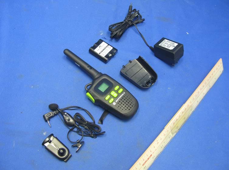
K7GMDBJJPR
Jun 24, 2012Two Way Radio - FRS
Equipment Class
FRF - Part 95 Family Radio Face Held Transmitter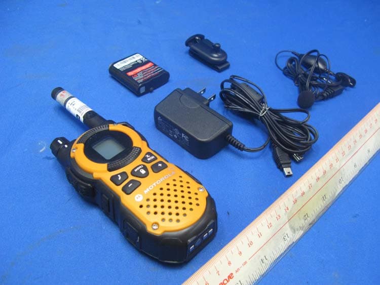
K7GMTCEJ
Apr 26, 2012Two Way Radio with GMRS and FRS
Equipment Class
CXX - Communications Rcvr for use w/ licensed Tx and CBs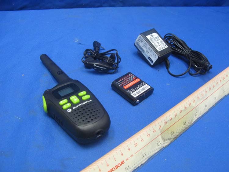
K7GMDBJJ
Mar 01, 2012Two Way Radio with GMRS and FRS
Equipment Class
FRF - Part 95 Family Radio Face Held Transmitter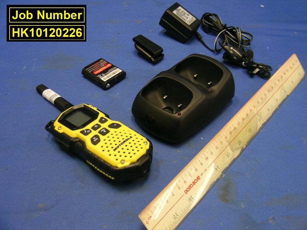
K7GMSFGJ
Mar 10, 2011Two Way Radio with Weather Band
Equipment Class
CXX - Communications Rcvr for use w/ licensed Tx and CBs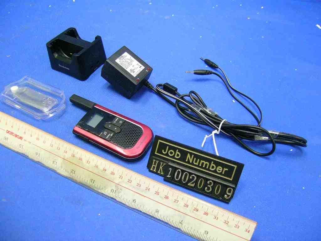
K7GT2007
Apr 08, 2010Two Way Radio with GMRS and FRS
Equipment Class
FRF - Part 95 Family Radio Face Held Transmitter