K7GT5525FRS
Giant Electronics Ltd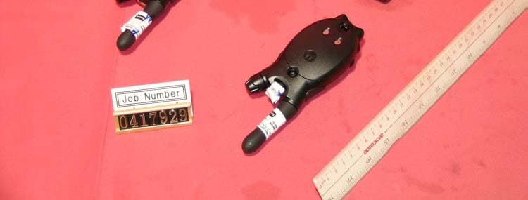
Click to zoom
Application Details
- Equipment Class
- FRF - Part 95 Family Radio Face Held Transmitter
- Date of Grant
- Nov 10, 2004
- Application Purpose
- Original Equipment
- Date of Application
- Nov 10, 2004
- Equipment Note
- FRS
- Frequency Range
- 462.56250000 - 467.71250000
- Company
- Giant Electronics Ltd
- Country
- Hong Kong
Documents & Files
Document Text
Text extracted from the exhibit documents filed with the FCC. Open a document above to read the original.
Users Manual
User's Guide FRS/RECREATIONAL TWO-WAY RADIOS KEM-PK10751-06 Models T5025 and T5525 Contents Contents Safety and General Information ...................... 2Control Buttons..................................................11Getting Started ..................................................12 Installing the the AA Batteries ........................12 Installing the NiCd Battery Pack ....................12 Battery Meter ....................................................13 Attaching the Belt Clip ....................................14 Removing the Belt Clip ....................................14 Turning Your Radio On and Off ......................14 Setting the Volume ..........................................14 Setting a Channel ............................................15 Talking and Listening ........................................16 Talk Range ........................................................16 Checking the Channel Before Transmitting ..16 Special Features ................................................17 Interference Eliminator Code ..........................17 Push to Talk Timeout Timer ............................17 Locking the Keypad ........................................17 Scanning Channels ..........................................18 Advanced Scan ................................................18 Alerts ..................................................................19 Channel Busy Indicator ..................................19 Setting and Transmitting Call Tones ..............19 Transmitting a Talk Confirmation Tone ..........20 QT Noise Filtering ............................................20 Accessories ........................................................22 Using Audio Accessories ................................22 Voice Activation (VOX) ....................................22 Setting the Sensitivity Level ..........................23 Patent Information ............................................24 1 Safety and General Information Safety and General InformationImportant Information on Safe and Efficient OperationRead This Information Before Using Your Radio.The information provided in this document supersedes the general safetyinformation in user guides published prior to December 1, 2002.Transmit and Receive ProcedureYour two-way radio contains a transmitter and a receiver. To control yourexposure and ensure compliance with the general population/uncontrolledenvironment exposure limits, always adhere to the following procedure:• Transmit no more than 50% of the time.• To transmit (talk), press the Push to Talk (PTT) button.• To receive calls, release the PTT button.Transmitting 50% of the time, or less, is important because the radio generatesmeasurable RF energy exposure only when transmitting (in terms of measuringstandards compliance).Exposure To Radio Frequency EnergyYour Motorola two-way radio complies with the following RF energy exposurestandards and guidelines:• United States Federal Communications Commission, Code of Federal Regulations; 47CFR part 2 sub-part J 2 Safety and General Information • American National Standards Institute (ANSI) / Institute of Electrical and Electronic Engineers (IEEE) C95. 1-1992 • Institute of Electrical and Electronic Engineers (IEEE) C95.1-1999 Edition • International Commission on Non-Ionizing Radiation Protection (ICNIRP) 1998 • Ministry of Health (Canada) Safety Code 6. Limits of Human Exposure to Radiofrequency Electromagnetic Fields in the Frequency Range from 3 kHz to 300 GHz, 1999 • Australian Communications Authority Radiocommunications (Electromagnetic Radiation --- Human Exposure) Standard, 2003 • ANATEL ANNEX to Resolution No. 303 of July 2, 2002 "Regulation of limitation of exposure to electrical, magnetic and electromagnetic fields in the radio frequencyrange between 9 KHz and 300 GHz" and "Attachment to resolution # 303 from July 2, 2002" To assure optimal radio performance and make sure human exposure to radiofrequency electromagnetic energy is within the guidelines set forth in the abovestandards, always adhere to the following procedures.Portable Radio Operation and EME Exposure Antenna CareUse only the supplied or an approved replacement antenna. Unauthorized antennas,modifications, or attachments could damage the radio and may violate FCC regulations.DO NOT hold the antenna when the radio is “IN USE.” Holding the antenna affects the effective range. 3 Safety and General Information Two-way Radio OperationWhen using your radio as a traditional two-way radio, hold the radio in a vertical position with the microphone 1 to 2 inches (2.5 to 5 cm)away from the lips. Body-Worn OperationTo maintain compliance with FCC/Health Canada RF exposure guidelines, if youwear a radio on your body when transmitting, always place the radio in a Motorola-supplied or approved clip, holder, holster, case, or body harness for this product.Use of non-Motorola-approved accessories may exceed FCC/Health Canada RFexposure guidelines.If you do not use one of the Motorola-supplied or approved body-worn accessories,and are not using the radio held in the normal use position, ensure the radio and its antenna are at least 1 inch (2.5 cm) from your body when transmitting. Data OperationIf applicable, when using any data feature of the radio with or without an accessorycable, position the radio and its antenna at least 1 inch (2.5 cm) from the body. Approved AccessoriesFor a list of approved Motorola accessories, visit our website at www.Motorola.com.Electromagnetic Interference/CompatibilityNote: Nearly every electronic device is susceptible to electromagnetic interference(EMI) if inadequately shielded, designed, or otherwise configured for electro-magnetic compatibility. 4 Safety and General Information FacilitiesTo avoid electromagnetic interference and/or compatibility conflicts, turn off yourradio in any facility where posted notices instruct you to do so. Hospitals or healthcare facilities may be using equipment that is sensi…
Text truncated - open the document above for the full version.
External Photos
Test Setup FCC ID : K7GT5525 External Photo - front External Photo - rear
ID Label/Location Info
Label Location FCC ID : K7GT5525 The label size and content follow the information in page 2 of this file.
Internal Photos
Test Setup FCC ID : K7GT5525 Internal Photo - 1 Internal Photo - 2 Test Setup FCC ID : K7GT5525 Internal Photo - 3 Internal Photo - 4 Test Setup FCC ID : K7GT5525 Internal Photo - 5
Parts List/Tune Up Info
GIANT ELECTRONICS LTD. Title: Alignment Procedure Model: T5025/T5525 Version: 00 THE CONTENT OF THIS DOCUMENT IS GIANT ELCT.LTD. INTELLECTUAL PROPERTY AND IS THE PROPERTY OF GIANT, IT IS TO BE TREATED AS STRICTLY AND IS NOT BE DISCLOSED, REPRODUCED, OR USED EXCEPT AS AUTHORIZED IN WRITING BY GIANT ELECTRONIC LTD. IN CONNECTION WITH THE MANUFACTURE, MAINTENANCE AND USE OF THE GIANT EQUIPMENT WHICH IT PERTAINS. COPYRIGHT @GIANT ELECT. LTD, ALL RIGHTS RESERVED tuneup.doc 1/5 A. PCB LEVEL (Test Condition: under CH8) NO ITEM ALIGNMENT METHOD REMARK 1. LCD display (Should enter test mode) 1. Press and hold the ‘+’ key and ‘Menu’ key together. 2. Turn on the radio power until a good key chirp is heard, and the backlight is on for about 500 ms . finally, the LCD should be display ‘1 CH ’. 3. Press ‘DOWN’ key , then all LCD segments should be anticlockwise displayed. 4. Finally, all the LCD segments should be shown for about 500ms as follows: 18 88. . 2. Standby current 1. Set A-METER, and RX mode. 2. Check the standby current <45mA DC. 3. Talk on current 1. Set A-METER, and TX mode @50ohm load. 2. Set channel to 14. 3. Check the talk on current <500mA DC. 4. VCO 1. Set RX or TX mode 2. Check TP103 to provide 0.7 ~ 2.4VDC. 3. Adjust L113 to provide 2.0 ± 0.1VDC at TP103 if VCO level are more than 2.4VDC on CH14. 5. TX Power (For 5525) 1. Set TX mode channel 7 and check the transmitted power < 0.04W (ERP) FRS 2. Set TX mode channel 8 and check the transmitted power < 0.02W (ERP) FRS (For 5025) 1. Set TX mode channel 7 and check the transmit power < 0.21W (ERP) FRS 2. Set TX mode channel 8 and check the transmit power < 0.12W (ERP) FRS Test voltage is 4.5V DC. 6. CTCSS Tone Frequency 1.Set CH1/CODE1. 2.Set Tx mode. 3.Check TP140 to be within 66.8Hz to 67.2Hz. 7. TX Frequency Adjust C159 to provide 462.5620MHz ± 50Hz. 8. CTCSS Tone Dev. 1. Set CH1/CODE1?AF input level to off, check DEV to be 350Hz~ 600Hz. 2. Set CH14/CODE38?AF input level to off, check DEV to be 350Hz~ 600Hz. FILTER SET: 1.50HZ~3KHZ 2.750 μ s De-emp ON 3. PK+ 4. FM DEV. AVG ON 9. TX Modulation & distortion 1.Set AF level at 25mv;1KHz, Adjust VR101 to provide Max TX deviation 2.25KHz to 2.35KHz. 2.Check input Mic level in 0.5~10 mV to provide normal deviation 1.5KHz. 3.Check the demodulation distortion <= 5%. 5. Audio Frequency Response. a) Input a 2.0mV 1KHz audio frequency to TP116 and press ‘PTT’ switch. b) Check the response compare to 1KHz tone. i) 500Hz : -5.0 dB to –11.0 dB. ii) 2.5KHz : +3.0 dB to +9.0 dB . Fliter set : 1.HPF 50Hz 2.LPF 15KHz 3. PK + All input at TP116 GIANT ELECTRONICS LTD. Title: Alignment Procedure Model: T5025/T5525 Version: 00 THE CONTENT OF THIS DOCUMENT IS GIANT ELCT.LTD. INTELLECTUAL PROPERTY AND IS THE PROPERTY OF GIANT, IT IS TO BE TREATED AS STRICTLY AND IS NOT BE DISCLOSED, REPRODUCED, OR USED EXCEPT AS AUTHORIZED IN WRITING BY GIANT ELECTRONIC LTD. IN CONNECTION WITH THE MANUFACTURE, MAINTENANCE AND USE OF THE GIANT EQUIPMENT WHICH IT PERTAINS. COPYRIGHT @GIANT ELECT. LTD, ALL RIGHTS RESERVED tuneup.doc 2/5 A. PCB LEVEL (Test Condition: under CH8) NO ITEM ALIGNMENT METHOD REMARK 10. VOX Detector (For T5525) 1.Set VOX level at 1. 2.Set AF level at 15.4 +/-0.2 mV,1KHz at TP116. 3. Unit start to transmit. 4.Set AF level at 13.5 +/-0.2 mV,1KHz at TP116. 5.Unit start to transmit. 6. Set VOX level at 2. 7.Set AF level at 9.4 +/-0.2 mV,1KHz at TP116. 8.Unit start to transmit. 9.Set AF level at 5.8 +/-0.2 mV,1KHz at TP116. 10.Unit start to transmit. 11.Set VOX level at 3. 12.Set AF level at 4.0 +/-0.2 mV,1KHz at TP116. 13.Unit start to transmit. 14.Set AF level at 2.7 +/-0.2 mV,1KHz at TP116. 15.Unit start to transmit. 11. Rx Audio test 1. Set RX mode CH7. 2. Set SG RF level to –50dBm with 1.5KHz deviation 1KHz modulation Signal. 3. Rotate the volume switch to the position, which give a Max audio output at TP117. 4. Check Max audio output level >1300mV. 5. Check Rx current <150mA. 6. Check the 1KHz distortion <= 5%. 7. Set SG RF level to –119dBm with 1.5kHz deviation at 1KHz audio frequency. a). Check SINAD sensitivity <= -119dBm. @12dB SINAD at TP117. 8. Audio frequency response. a) Set SG RF level to –50dBm with 1.5kHz deviation at 1KHz audio frequency. b) Rotate the volume switch to the position, which give an output 100mV±5mV at TP117. c) Vary the audio frequency from 300Hz to 3KHz. d) Check the RX response compare to 1KHz tone. i) 500Hz : +1.0 dB to +5.0 dB. ii) 2.5KHz : -10.0 dB to –18.0 dB. 9. Maximum and Minimum Audio Output Power. a) Set SG RF level to –50dBm with 1.5kHz deviation at 1KHz audio frequency. b) Rotate the volume switch to the position, which give a maximum output . c) Check the voltage at TP117 >/=1500mV. d) Set maximum audio output to 0dB, rotate the volume switch to the position, which give a minimum output. e) Check the minimum voltage -23dB to -40dB at TP117 12. Noise- Detector 1. Set SG to –120dBm with 1.5KHz deviation., 1KHz AF on CH7. 2. Adjust VR102 for transient state @ 10dB SINAD. 3. Check high state @8 to 13dB SINAD. GIANT ELECTRONICS LTD. Title: Alignment Procedure Model: T5025/T5525 Version: 00 THE CONTENT OF THIS DOCUMENT IS GIANT ELCT.LTD. INTELLECTUAL PROPERTY AND IS THE PROPERTY OF GIANT, IT IS TO BE TREATED AS STRICTLY AND IS NOT BE DISCLOSED, REPRODUCED, OR USED EXCEPT AS AUTHORIZED IN WRITING BY GIANT ELECTRONIC LTD. IN CONNECTION WITH THE MANUFACTURE, MAINTENANCE AND USE OF THE GIANT EQUIPMENT WHICH IT PERTAINS. COPYRIGHT @GIANT ELECT. LTD, ALL RIGHTS RESERVED tuneup.doc 3/5 A. PCB LEVEL (Test Condition: under CH8) NO ITEM ALIGNMENT METHOD REMARK 13. CTCSS tone Detect 1. Set CH7/CODE1and SG to –122dBm with 67Hz tone frequency, 400Hz deviation. 2. Check the Pin31 of IC105 to have square-wave, and low for RF modulation off. 3. Repeat item 1 and 2 for code38(250.3Hz). 4. Repeat item 1 and 3 for CH14. 14. Quiet tone det 1.Set unit to quiet noise mode. 2.Set CH1/CODE 1and SG to –60dBm with 67Hz tone frequency, 400Hz deviation and 55Hz audio frequency, 400Hz deviatio…
Text truncated - open the document above for the full version.
Parts List/Tune Up Info
Giant Electronics Ltd. T5525 FRS RADIO EABASE UNIT (ALL) 1 EABASE CASING (ALL) 1 EABASE CASING COMMON 1 EAANTENNA WIRE 1 EABATT PALTE "-" 1 EABATT PLATE "+" "-" (A) 1 EABATT PLATE "-" "+" (B) 1 EACHARGING CONTACT 2 EAMETAL DOME FOR KEYPAD 1 EADOUBLE ADHESIVE TAPE FOR KEYPAD 1 EAMIC CUSHION COVER 1 EASPEAKER NET 1 EASPEAKER SPONGE 1 EATAPTITE SCREW X/HD T2.3X8 2 EATAPTITE SCREW X/HD T2.3X10 2 EABASE RF & MAIN (ALL) 1 EAKEYPAD T5500 BLACK 1 EAPTT RUBBER BUTTON BLACK 1 EAFRONT HOUSING BLACK 1 EAFRONT HOUSING BLACK 2# 0 EAREAR HOUSING BLACK 2# 0 EAREAR HOUSING BLACK 1 EABATTERY DOOR BLACK 1 EABATTERY DOOR BLACK 3# 0 EAFRONT COVER ROSEWOOD 1 EAPRINTING FOR FRONT COVER 1 EAFRONT COVER W/O PRINTING ROSEWOOD 1 EAFRONT COVER ROSEWOOD 2# 0 EAPRINTING FOR FRONT COVER 2# 1 EA E:FRONT COVER W/O PRINTING ROSEW 1 EA E:VOLUME KNOB 1 EAVOLUME KNOB W/O PRINTING BLACK 1 EAPRINTING FOR VOLUME KNOB 1 EAJACK COVER BLACK 1 EAANTENNA RUBBER CAP BLACK 1 EALCD LENS 1 EAINDICATOR LENS 1 EABELT CLIP COVER BLACK 1 EAANTENNA INSERT 1 EAPTT INSERT BLACK 1 EABASE RF & MAIN PCB (ALL) 1 EABASE CASING COMMON PARTS 1 EASTRAND WIRE UL1007 #28 BLACK 0.038 M JW201STRAND WIRE UL1007 #28 RED 0.037 M JW201SPEAKER 32 OHM 0.5W 3632A505 1 EA SPK101MIC DB MIC C9745 42dB 1 EA MIC101BASE RF MAIN COMMON PART 1 EABATT PLATE "+" 1 EA T5525..T5525 1//7 Giant Electronics Ltd. LCD BRACKET FOR 1W 1 EAVCO SHIELD CAN OFIW 1 EAVCO SHIELD CAN COVER 1 EAWHITE SHEET FOR RUBBER 1 EALCD CUSHION 2 EALCD LIGHT GUIDE 1 EABASE RF & MAIN PCB SMT COMMON PARTS 1 EAPCB RF 95.5X49.1X1MM FR4 DS 1 EABASE RF & MAIN PCB SMT BOTTOM COMMON PART 1 EACAP CER CHIP 50V COG +/-5% 100PF EYANG 4 EA C231,C251,C210,C19CAP.CER.CHIP 50V CH J% 100PF MURATA 0 EA C231,C251,C210,C19CAP CER CHIP 50V X7R +/-10% 0.001u EYANG 5 EA C113,C148,C164,C214,R198CAP.CER.CHIP 50V B K% 0.001UF MURATA 0 EA C113,C148,C164,C214,R198CAP CER CHIP 16V X7R +/-10% 0.01uF EYANG 2 EA C192,C257CAP. CER. CHIP 16V X7R K 0.01UF 0 EA C192,C257CAP. CER. CHIP 50V B K% 0.01UF 1 EA C194CAP CER CHIP 16V Y5V Z 0.1uF EYANG 7 EA C170,C173,C175,C204,C207,C264,C10CAP.CER.CHIP 16V F Z% 0.1UF MURATA 0 EA C170,C173,C175,C204,C207,C264,C10CAP. CER. CHIP 10V Y5V Z% 1UF 1 EA C200CAP. CER. CHIP 16V F Z% 1UF 1 EA C152CAP.CER.CHIP 50V CH C% 1PF MURATA 0.3 EA C179 FOR MATCH YELLOW/B3 CRYSTALCAP.CER.CHIP 50V CH J% 12PF MURATA 0.3 EA C180 FOR MATCH WHITE/B1 CRYSTALCAP.CER.CHIP 16V B K% 0.012UF MURATA 1 EA C184CAP.CER.CHIP 50V CH J% 15PF MURATA 0.75 EA C180 MATCH BLACK/YELLOW/B3 CRYSTAL C171 FOR MATCH GREEN/B4 CRYSTAL CAP. CER. CHIP 50V CH J% 150P F 1 EA C274CAP. CER. CHIP 50V B K% 0.0015UF 1 EA C163CAP.CER.CHIP 50V CH C% 1.5PF MURATA 1 EA C123CAP.CER.CHIP 50V CH J% 18PF MURATA 0.15 EA C180 FOR MATCH B4 CRYSTALCAP. CER. CHIP 50V CH J% 20PF MURATA 0.45 EA C180 FOR MATCH GREEN CRYSTAL C171 FOR MATCH BLACK/B1 CRYSTAL CAP.CER.CHIP 50V CH C% 2PF MURATA 0.6 EA C165 MATCH BLACK/WHITE/GREEN C179 FOR MATCH WHITE CRYSTAL CAP.CER.CHIP 50V CH J% 22PF MURATA 0.45 EA C171 MATCH YELLOW/WHITE/B3 CRYSTALCAP.CER.CHIP 50V B K% 0.0022UF MURATA 1 EA C161CAP.CER.CHIP 16V B K% 22NF MURATA 6 EA C196,C228,C239,C258,C6,C7CAP. CER. CHIP 50V NPO J 27P 0402 2 EA C190,C155CAP. CER. CHIP 10V X7R K 0.027UF 0 EA R1CAP CER CHIP 16V X7R K 0.027UF EYANG 1 EA R1CAP.CER. CHIP 50V NPO J% 30pF 1 EA C133CAP.CER.CHIP 50V CH C% 3PF MURATA 1 EA C114CAP. CER. CHIP 16V B K% 0.33UF 1 EA C186CAP CER CHIP 50V NPO J% 39PF MURATA 1 EA C202CAP CER CHIP 50V NPO J 390PF 1 EA C187CAP.CER.CHIP 50V CH C% 4PF MURATA 0.15 EA C165 FOR MATCH B4 CRYSTALCAP CER CHIP 50V NPO J% 47PF MURATA 1 EA C201CAP. CER. CHIP 10V X7R K 0.047UF 3 EA C118,C256,C162,E:CAP. CER. CHIP 50V CH C% 5PF MURATA 0.15 EA C165 FOR MATCH B1 CRYSTALCAP.CER. CHIP 50V NPO J% 56pF 1 EA C199 T5525..T5525 2//7 Giant Electronics Ltd. CAP CER CHIP 25V X7R +/-10% 560PF EYANG 2 EA C185,C122CAP. CER. CHIP 50V B K% 560PF 0 EACAP CER CHIP 25V XTR +/-10% 5 6nF EYANG 2 EA C241,C5CAP. CER. CHIP 25V B K% 0.0056UF MURATA 0 EA C241,C5CAP. CER. CHIP 10V X7R K 0.056UF 0 EA C191CAP CER CHIP 10V X5R K 0.056UF EYANG 1 EA C191CAP. CER. CHIP 50V U2J J% 62PF 1 EA C176CAP. CER. CHIP 50V CH C% 7PF MURATA 1 EA C131CAP. CER. CHIP 50V CH C% 8PF MURATA 1 EA C130CAP. CER. CHIP 50V B K 820PF 0603 MURATA 1 EA C225LED CHIP KPA-3010EC RED 2 EA D2,D108LED CHIP KPT-2012EC RED 1 EA D109DIODE PIN 1SS314 1 EA D106INDUCTOR CHIP 27NH +-5% SDCL1608C27NJ 1 EA L107INDUCTOR CHIP 33NH +-5% LQG18HN33NJ00D 1 EA L110THER. NTCCM10053EH220JC TDK 0402 TYPE 1 EA TR102RES. CHIP 1/16W 0 OHM 2 EA R296,C222RES. CHIP 1/16W 1K 3 EA R270,R215,R199,R147FOR MATCH KEIC-S1T3361DRES. CHIP 1/16W 10K 2 EA R168,R187RES. CHIP 1/16W 100K 3 EA R102,R241,R12RES. CHIP 1/16W 1M 1 EA R206RES CHIP 1/16W 1.1M 5% 1 EA R167RES. CHIP 1/16W 1.2K 1 EA R123RES CHIP 1/16W 5% 120K 0402 1 EA R145RES. CHIP 1/16W 13K 0402 2 EA R156,R161RES. CHIP 1/16W 130K 1 EA R148RES CHIP 1/16S 5% 1.3M 0402 1 EA R186RES. CHIP 1/16W 15K 1 EA R195RES. CHIP 1/16W 5% 150K 0402 2 EA R146,R213RES. CHIP 1/16W 180 0402 1 EA R189RES. CHIP 1/16W 200K 1 EA R30RES. CHIP 1/16W 220 1 EA R127RES. CHIP 1/16W 2.2K 1 EA R13RES. CHIP 1/16W 2.2K 1 EA R259RES. CHIP 1/16W 22K 4 EA R243,R204,R11,C205RES. CHIP 1/16W 220K 2 EA R154,R196,R141FOR MATCH KEIC-S1T3361DRES. CHIP 1/16W 270 OHM 0402 1 EA R188RES. CHIP 1/16W 270K 0402 4 EA R155,R185,R214,R141FOR MATCH KEIC-YD3361RES. CHIP 1/16W 3K 1 EA R151RES. CHIP 1/16W 33 1 EA R231RES. CHIP 1/16W 330 OHM 0402 1 EA R262RES. CHIP 1/16W 3.3K 0402 1 EA R107RES. CHIP 1/16W 33K 2 EA R160,R244RES. CHIP 1/16W 5% 330K 0402 2 EA R153,R172RES. CHIP 1/16W 390 1 EA R297RES. CHIP 1/16W 3.9K 2 EA R131,R184RES CHIP 1/16W 5% 390K 0402 1 EA R14RES. CHIP 1/16W 4.7K 0402 2 EA R211,R224RES. CHIP 1/16W 47K 3 EA R144,R200,C203 T5525..T5525 3//7 Giant Electronics Ltd. RES. CHIP 1/16W 470K 0402 12 EA R117,R132,R157,R192,R208,R209,R210,R221,R222,R223 R163,R10 RES. CHIP 1/16W 51K 1 EA R158RES. CHIP 1/16W 5.6K 0402 1 EA R147FOR MATCH KEIC-YD3361RES. CHIP 1/16W 6.8K 0402 1 EA R140TR.CHIP PNP 2SA1980UF SOT-323F 1 EA Q111TR CHIP PNP 2S…
Text truncated - open the document above for the full version.
Test Report
• The test results reported in this report shall refer only to the sample actually tested and shall not refer or be deemed a refer to bulk from which such a sample may be said to have been obtained. • This report shall not be reproduced except in full without prior authorization from Intertek Testing Services Hong Kong Limited • For Terms And Conditions of the services, it can be provided upon request. • The evaluation data of the report will be kept for 3 years from the date of issuance. Intertek Testing Services Hong Kong Ltd. 2/F., Garment Centre, 576 Castle Peak Road, Kowloon, Hong Kong. Tel: (852) 2173 8888 Fax: (852) 2371 0521 Website: www.hk.intertek-etlsemko.com Giant Electronics Limited Application For Certification (FCC ID: K7GT5525) October 28, 2004 0417929 TL/ Ann Choy October 28, 2004 INTERTEK TESTING SERVICES FCC ID: K7GT5525 i SUMMARY OF CONTENTS LIST OF EXHIBITS EXHIBIT 1: General Description EXHIBIT 2 : System Test Configuration EXHIBIT 3: RF Power Output EXHIBIT 4: Modulation Characteristics EXHIBIT 5: Occupied Bandwidth EXHIBIT 6: Spurious Emission EXHIBIT 7: Frequency Stability EXHIBIT 8: Technical Specifications EXHIBIT 9: Product Labelling EXHIBIT 10: Photographs EXHIBIT 11: Instruction Manual EXHIBIT 12: Tune Up Procedure EXHIBIT 13: Part List EXHIBIT 14: Input Current EXHIBIT 15: RF Exposure Info EXHIBIT 16: Confidentiality Request INTERTEK TESTING SERVICES FCC ID: K7GT5525 ii MEASUREMENT/TECHNICAL REPORT Application : Giant Electronics Limited Trade Name/Model No : Giant / Motorola T5525 Date : October 28, 2004 This report concerns (check one:)Original Grant X Class II Change Equipment Type: Family Radio Service, FRS Deferred grant requested per 47 CFR 0.457(d)(1)(ii)? Yes No X If yes, defer until: date Company Name agrees to notify the Commission by: date of the intended date of announcement of the product so that the grant can be issued on that date. Report prepared by: Tommy Leung Intertek Testing Services 2/F., Garment Centre, 576 Castle Peak Road, Kowloon, Hong Kong. Phone: 852-2173-8536 Fax: 852-2741-1693 INTERTEK TESTING SERVICES FCC ID: K7GT5525 iii Table of Contents 1.0 General Description..............................................................................................2 1.1 Product Description ..........................................................................................2 1.2 Related Submittal(s) Grants.............................................................................3 1.3 Test Methodology.............................................................................................3 1.4 Test Facility ......................................................................................................3 2.0 System Test Configuration ...................................................................................5 2.1 Justification .......................................................................................................5 2.2 EUT Exercising Software .................................................................................6 2.3 Special Accessories .........................................................................................6 2.4 Measurement Uncertainty................................................................................6 2.5 Equipment Modification ....................................................................................6 3.0 RF Output Power (Section 95.639(d)) ..................................................................8 4.0 Modulation Characteristics (Section 95.637(a)) ................................................13 4.1 Modulation Frequiency Response ..................................................................14 4.2 Modulation Limiting Characteristic ..................................................................16 4.3 Audio Low Pass Filter Response ...................................................................18 5.0 Occupied Bandwidth (Section 95.633(c)) ........................................................20 6.0 Spurious Emission (Section 95.635(b)) .............................................................22 6.1 Field Strength of Spurious Radiation...............................................................23 7.0 Frequency Stability (Section 95.627).................................................................31 7.1 Frequency Tolerance ......................................................................................32 7.2 Temperature Extreme Condition .....................................................................34 7.3 Voltage Extreme Condition .............................................................................37 8.0 Technical Specifications....................................................................................40 9.0 Product Labelling................................................................................................44 10.0 Equipment Photographs..................................................................................47 11.0 Instruction Manual............................................................................................49 12.0 Tune Up Procedure...........................................................................................51 13.0 Part List.............................................................................................................53 14.0 Input Current .....................................................................................................55 15.0 RF Exposure Info ..............................................................................................57 16.0 Confidentiality Request ....................................................................................59 INTERTEK TESTING SERVICES FCC ID: K7GT5525 iv List of attached file Exhibit type File Description Filename Operation Description Technical Description descri.pdf Test Report Bandwidth Plot bw.pdf Test Report Modulation Frequency Response mfr.pdf Test Re…
Text truncated - open the document above for the full version.
Test Setup Photos
The Worst Case Configuration Photographs FCC ID: K7GT5525 Radiated Emission Front View Rear View The Worst Case Configuration Photographs FCC ID: K7GT5525 Radiated Emission Front View Rear View
Contact Information
Applicant
Yumin Zou(A. Manager)
Technical Contact
Intertek Testing Services Hong Kong Ltd.Tommy Leung
[email protected]852-2173-8538
2/F., Garment Centre, · Kowloon · Hong Kong
Non-Technical Contact
Intertek Testing Services Hong Kong Ltd.Tommy Leung
[email protected]852-2173-8538
Test Firm
Intertek Testing Services Hong KongBilly Chow
Technical Specifications
| # | Rule Parts | Frequency Range | Power Output | Emission | Tolerance |
|---|---|---|---|---|---|
| 1 | 95B | 462.5625 MHz - 467.7125 MHz | 40.00 mW | 5K85F3E | 0.9700000000 ppm |
Other Applications from Giant Electronics Ltd
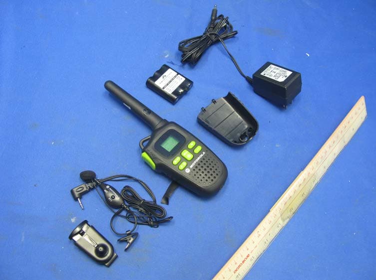
K7GMDBJJPR
Jun 24, 2012Two Way Radio - FRS
Equipment Class
FRF - Part 95 Family Radio Face Held Transmitter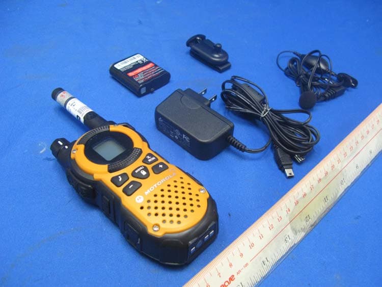
K7GMTCEJ
Apr 26, 2012Two Way Radio with GMRS and FRS
Equipment Class
CXX - Communications Rcvr for use w/ licensed Tx and CBs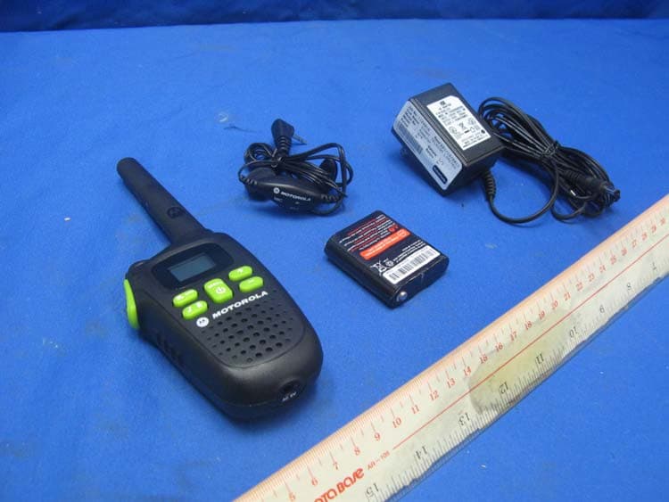
K7GMDBJJ
Mar 01, 2012Two Way Radio with GMRS and FRS
Equipment Class
FRF - Part 95 Family Radio Face Held Transmitter
K7GMSFGJ
Mar 10, 2011Two Way Radio with Weather Band
Equipment Class
CXX - Communications Rcvr for use w/ licensed Tx and CBs
K7GT2007
Apr 08, 2010Two Way Radio with GMRS and FRS
Equipment Class
FRF - Part 95 Family Radio Face Held Transmitter