K7GT8230FRS+GMRS
Giant Electronics Ltd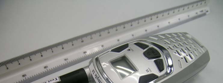
Click to zoom
Application Details
- Equipment Class
- FRF - Part 95 Family Radio Face Held Transmitter
- Date of Grant
- Jun 28, 2004
- Application Purpose
- Original Equipment
- Date of Application
- Jun 28, 2004
- Equipment Note
- FRS+GMRS
- Frequency Range
- 467.56250000 - 467.71250000
- Company
- Giant Electronics Ltd
- Country
- Hong Kong
Documents & Files
Document Text
Text extracted from the exhibit documents filed with the FCC. Open a document above to read the original.
External Photos
Test Setup FCC ID : K7GT8230 External Photo -front External Photo - rear
Internal Photos
Test Setup FCC ID : K7GT8230 Internal Photo – 1 Internal Photo - 2 Test Setup FCC ID : K7GT8230 Internal Photo - 3 Internal Photo - 4
Parts List/Tune Up Info
Giant Electronics Ltd. Title: Alignment Procedure Model: T8230 Version 00 The content of this document is Giant Electronics Ltd.'s intellectual property and is the property of Giant. It is to be treated as strictly confidential and is not to be disclosed, reproduced, or used except as authorized in writing by Giant Electronics Ltd. In connection with the manufacture, maintenance and use of the Giant equipment to which it pertains. Copyright @Giant Electronics Ltd. All rights reserved. 8230_ALIGNMENT PROCEDURE v02.doc page1of 5 A. PCB LEVEL (Test Condition: under CH15) NO ITEM ALIGNMENT METHOD REMARK 1. LCD display (Should enter test mode) 1. Press and hold the ‘+’ key and ‘Menu’ key together. 2. Turn on the radio power until a good key chirp is heard, and the backlight is on for about 500 ms . finally, the LCD should be display ‘1 CH ’. 3. Press ‘DOWN’ key , then all LCD segments should be anticlockwise displayed. 4. Finally, all the LCD segments should be shown for about 500ms as follows: 18 88. . 2. Standby current 1. Set A-METER, and RX mode. 2. Check the standby current <45mA DC. 3. Talk on current 1. Set A-METER, and TX mode @50ohm load. 2. Check the talk on current <900mA DC. 3. Set channel to 14. 4. Check the talk on current <500mA DC. 4. VCO 1. Set RX or TX mode 2. Check TP103 to provide 0.7 ~ 2.4VDC. 3. Adjust L113 to provide 2.0 ± 0.1VDC at TP103 if VCO level are more than 2.4VDC on CH14. 5. TX Power 1. Set TX mode CH15. 2. Check transmit power to provide <0.23WERP. 3. Set TX mode channel 14. 4. Adjust VR 1 to provide <0.14WERP. Test voltage is 4.5V DC. 6. CTCSS Tone Frequency 1.set CH1/CODE1. 2.Set Tx mode. 3.Check TP140 to be within 66.8Hz to 67.2Hz. 7. TX Frequency Adjust C159 to provide 462.5620MHz ± 50Hz. 8. CTCSS Tone Dev. 1. Set CH1/CODE1?AF input level to off, check DEV to be 350Hz~ 600Hz. 2. Set CH14/CODE38?AF input level to off, check DEV to be 350Hz~ 600Hz. FILTER SET: 1.50HZ~3KHZ 2.750μs De-emp ON 3. PK+ 4. FM DEV. AVG ON 9. TX Modulation & distortion 1.Set AF level at 25mv;1KHz,Adjust VR101 to provide Max TX deviation 2.25KHz to 2.35KHz. 2.Check input Mic level in 0.5~10 mV to provide normal deviation 1.5KHz. 3.Check the demodulation distortion <= 5%. 5. Audio Frequency Response. a) Input a 2.0mV 1KHz audio frequency to TP116 and press ‘PTT’ switch. b) Check the response compare to 1KHz tone. i) 500Hz : -5.0 dB to –11.0 dB. ii) 2.5KHz : +3.0 dB to +9.0 dB . Fliter set : 1.HPF 50Hz 2.LPF 15KHz 3. PK + All input at TP116 Giant Electronics Ltd. Title: Alignment Procedure Model: T8230 Version 00 The content of this document is Giant Electronics Ltd.'s intellectual property and is the property of Giant. It is to be treated as strictly confidential and is not to be disclosed, reproduced, or used except as authorized in writing by Giant Electronics Ltd. In connection with the manufacture, maintenance and use of the Giant equipment to which it pertains. Copyright @Giant Electronics Ltd. All rights reserved. 8230_ALIGNMENT PROCEDURE v02.doc page2of 5 A. PCB LEVEL (Test Condition: under CH15) NO ITEM ALIGNMENT METHOD REMARK 10. VOX Detector 1.Set VOX level at 1. 2.Set AF level at 15.4 +/-0.2 mV,1KHz at TP116. 3. Unit start to transmit. 4.Set AF level at 13.5 +/-0.2 mV,1KHz at TP116. 5.Unit start to transmit. 6. Set VOX level at 2. 7.Set AF level at 9.4 +/-0.2 mV,1KHz at TP116. 8.Unit start to transmit. 9.Set AF level at 5.8 +/-0.2 mV,1KHz at TP116. 10.Unit start to transmit. 11.Set VOX level at 3. 12.Set AF level at 4.0 +/-0.2 mV,1KHz at TP116. 13.Unit start to transmit. 14.Set AF level at 2.7 +/-0.2 mV,1KHz at TP116. 15.Unit start to transmit. 11. Rx Audio test 1. Set RX mode CH7. 2. Set SG RF level to –50dBm with 1.5KHz deviation 1KHz modulation Signal. 3. Adjust L114 to provide minimum distortion & max output level at TP117. 4. Rotate the volume switch to the position, which give a Max audio output at TP117. 5. Check Max audio output level >1500mV. 6. Check Rx current <150mA. 7. Check the 1KHz distortion <= 5%. 8. Set SG RF level to –119dBm with 1.5kHz deviation at 1KHz audio frequency. a). Check SINAD sensitivity <= -119dBm. @12dB SINAD at TP117. 9. Audio frequency response. a) Set SG RF level to –50dBm with 1.5kHz deviation at 1KHz audio frequency. b) Rotate the volume switch to the position, which give an output 100mV±5mV at TP117. c) Vary the audio frequency from 300Hz to 3KHz. d) Check the RX response compare to 1KHz tone. i) 500Hz : +1.0 dB to +5.0 dB. ii) 2.5KHz : -10.0 dB to –18.0 dB. 10. Maximum and Minimum Audio Output Power. a) Set SG RF level to –50dBm with 1.5kHz deviation at 1KHz audio frequency. b) Rotate the volume switch to the position, which give a maximum output . c) Check the voltage at TP117 >/=1500mV. d) Set maximum audio output to 0dB, rotate the volume switch to the position, which give a minimum output. e) Check the minimum voltage -23dB to -40dB at TP117 12. Noise- Detector 1. Set SG to –120dBm with 1.5KHz deviation., 1KHz AF on CH7. 2. Adjust VR102 for transient state @ 10dB SINAD. 3. Check high state @8 to 13dB SINAD. Giant Electronics Ltd. Title: Alignment Procedure Model: T8230 Version 00 The content of this document is Giant Electronics Ltd.'s intellectual property and is the property of Giant. It is to be treated as strictly confidential and is not to be disclosed, reproduced, or used except as authorized in writing by Giant Electronics Ltd. In connection with the manufacture, maintenance and use of the Giant equipment to which it pertains. Copyright @Giant Electronics Ltd. All rights reserved. 8230_ALIGNMENT PROCEDURE v02.doc page3of 5 A. PCB LEVEL (Test Condition: under CH15) NO ITEM ALIGNMENT METHOD REMARK 13. CTCSS tone Detect 1. Set CH15/CODE1and SG to –122dBm with 67Hz tone frequency, 400Hz deviation. 2. Check the Pin31 of IC105 to have square-wave, and low for RF modulation off. 3. Repeat item 1 and 2 for code38(250.3Hz). 4. Repeat item 1 and 3 for CH14. 14. Quiet tone det 1.Set unit to quiet noise mode. 2.Set CH15/CODE 1and SG to –…
Text truncated - open the document above for the full version.
Test Report
• The test results reported in this report shall refer only to the sample actually tested and shall not refer or be deemed a refer to bulk from which such a sample may be said to have been obtained. • This report shall not be reproduced except in full without prior authorization from Intertek Testing Services Hong Kong Limited • For Terms And Conditions of the services, it can be provided upon request. • The evaluation data of the report will be kept for 3 years from the date of issuance. Intertek Testing Services Hong Kong Ltd. 2/F., Garment Centre, 576 Castle Peak Road, Kowloon, Hong Kong. Tel: (852) 2173 8888 Fax: (852) 2371 0521 Website: www.hk.intertek-etlsemko.com E Giant Electronics Ltd. Application For Certification (FCC ID: K7GT8230) March 18, 2004 0400264 DL/ Ann Choy March 18, 2004 INTERTEK TESTING SERVICES FCC ID: K7GT8230 i SUMMARY OF CONTENTS LIST OF EXHIBITS EXHIBIT 1: General Description EXHIBIT 2: System Test Configuration EXHIBIT 3: RF Power Output EXHIBIT 4: Modulation Characteristics EXHIBIT 5: Occupied Bandwidth EXHIBIT 6: Spurious Emission EXHIBIT 7: Frequency Stability EXHIBIT 8: Technical Specifications EXHIBIT 9: Product Labelling EXHIBIT 10: Photographs EXHIBIT 11: Instruction Manual EXHIBIT 12: Tune Up Procedure EXHIBIT 13: Part List EXHIBIT 14: Input Current EXHIBIT 15: RF Exposure Info EXHIBIT 16: Confidentiality Request INTERTEK TESTING SERVICES FCC ID: K7GT5000 iii Table of Contents 1.0 General Description..............................................................................................2 1.1 Product Description ..........................................................................................2 1.2 Related Submittal(s) Grants.............................................................................3 1.3 Test Methodology.............................................................................................3 1.4 Test Facility ......................................................................................................3 2.0 System Test Configuration...................................................................................5 2.1 Justification .......................................................................................................5 2.2 EUT Exercising Software .................................................................................6 2.3 Special Accessories .........................................................................................6 2.4 Measurement Uncertainty................................................................................6 2.5 Equipment Modification....................................................................................6 3.0 RF Output Power (Section 95.639(d))..................................................................8 4.0 Modulation Characteristics (Section 95.637(a)) ................................................12 4.1 Modulation Frequiency Response ..................................................................13 4.2 Modulation Limiting Characteristic ..................................................................15 4.3 Audio Low Pass Filter Response ...................................................................17 5.0 Occupied Bandwidth (Section 95.633(c)) .........................................................19 6.0 Spurious Emission (Section 95.635(b)).............................................................21 6.1 Field Strength of Spurious Radiation...............................................................22 7.0 Frequency Stability (Section 95.627) .................................................................28 7.1 Frequency Tolerance ......................................................................................29 7.2 Temperature Extreme Condition .....................................................................31 7.3 Voltage Extreme Condition .............................................................................34 8.0 Technical Specifications....................................................................................37 9.0 Product Labelling................................................................................................41 10.0 Equipment Photographs..................................................................................44 11.0 Instruction Manual............................................................................................46 12.0 Tune Up Procedure...........................................................................................48 13.0 Part List .............................................................................................................50 14.0 Input Current.....................................................................................................52 15.0 RF Exposure Info..............................................................................................54 16.0 Confidentiality Request....................................................................................56 INTERTEK TESTING SERVICES FCC ID: K7GT8230 iv List of attached file Exhibit type File Description Filename Operation Description Technical Description descri.pdf Test Report Bandwidth Plot bw.pdf Test Report Modulation Frequency Response mfr.pdf Test Report Modulation Limit Characteristic mlc.pdf Test Report Spurious Emission spurious.pdf Block Diagram Block Diagram block.pdf Schematics Circuit Diagram circuit.pdf ID Label/Location Label Artwork and Location label.pdf User Manual User Manual manual.pdf Test Report Test Report report.pdf Test Setup Photo Radiated Emission radiated photos.doc Internal Photo Internal Photo internal photos.doc External Photo External Photo external photos.doc Test Report Tune Up Procedure tuneup.pdf Test Report Part List partlist.pdf Test Report Audio Low Pass Filter Response lpf.pdf Cover Letter Confidentiality Request request.pdf INTERTEK TESTING SERVICES FCC ID: K7GT8230 1 EXHIBIT 1 GENERAL DESCRIPTION INTERTEK…
Text truncated - open the document above for the full version.
Test Report
Modulation Frequency Response 0.000.501.001.502.00 200 700 1200 1700 2200 2700 3200 3700 4200 4700 Modulation Frequency (Hz) Frequency Deviation (kHz) Modulation Frequency Response 0.000.501.001.50 300 800 1300 1800 2300 2800 3300 3800 4300 4800 Modulation Frequency (Hz) Modulation Index (%)
Test Report
Modulation Limiting Characteristic 0.000.501.001.502.002.50 47 57 67 77 87 97 107 117 127 137 Modulation Input (dBSPL) Frequency Deviation (kHz) 500Hz1000Hz2500Hz3125Hz
Test Report
Audio Low Pass Filter Response -60.0-50.0-40.0-30.0-20.0-10.0 0.0 10.0 1 10 100 Frequency (kHz) dB relative to 1 kHz LPF ResponseTIA/EIA-603
Test Setup Photos
Test Setup FCC ID : K7GT8230 Radiated -front Radiated - rear
Contact Information
Applicant
Yumin Zou(A. Manager)
Technical Contact
Intertek Testing Services Hong Kong Ltd.Derek Leung
[email protected]852-2173-8539
2/F., Garment Centre, · Kowloon · Hong Kong
Non-Technical Contact
Intertek Testing Services Hong Kong Ltd.Derek Leung
[email protected]852-2173-8539
Test Firm
Intertek Testing Services Hong KongBilly Chow
Technical Specifications
| # | Rule Parts | Frequency Range | Power Output | Emission | Tolerance |
|---|---|---|---|---|---|
| 2 | 95B | 467.5625 MHz - 467.7125 MHz | 140.00 mW | 10K4F3E | 2.5 ppm |
Other Applications from Giant Electronics Ltd
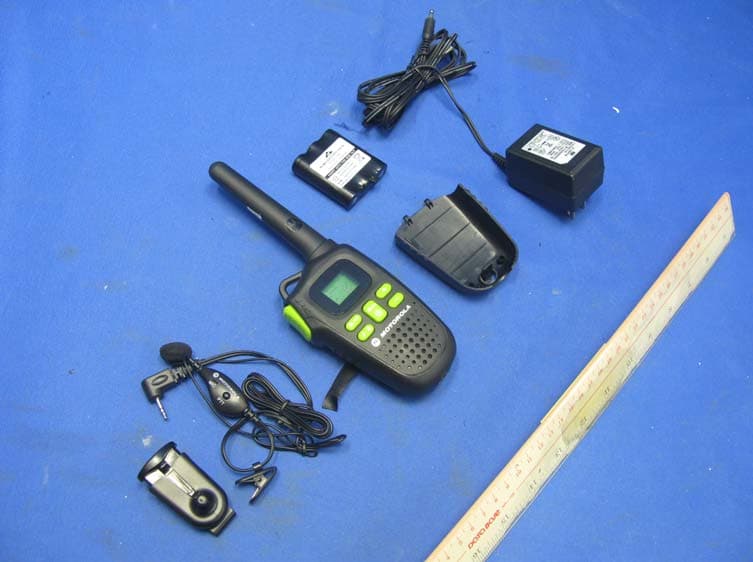
K7GMDBJJPR
Jun 24, 2012Two Way Radio - FRS
Equipment Class
FRF - Part 95 Family Radio Face Held Transmitter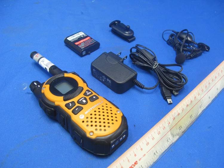
K7GMTCEJ
Apr 26, 2012Two Way Radio with GMRS and FRS
Equipment Class
CXX - Communications Rcvr for use w/ licensed Tx and CBs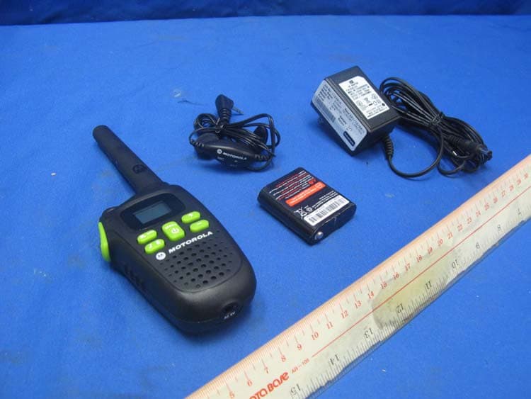
K7GMDBJJ
Mar 01, 2012Two Way Radio with GMRS and FRS
Equipment Class
FRF - Part 95 Family Radio Face Held Transmitter
K7GMSFGJ
Mar 10, 2011Two Way Radio with Weather Band
Equipment Class
CXX - Communications Rcvr for use w/ licensed Tx and CBs
K7GT2007
Apr 08, 2010Two Way Radio with GMRS and FRS
Equipment Class
FRF - Part 95 Family Radio Face Held Transmitter