KINAPG20FNETWireless LAN, AIRPRO GOLD 20F.NET
Wave Wireless Corporation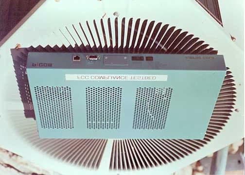
Click to zoom
Application Details
- Equipment Class
- DSS - Part 15 Spread Spectrum Transmitter
- Date of Grant
- Mar 13, 2002
- Application Purpose
- Original Equipment
- Date of Application
- Mar 13, 2002
- Equipment Note
- Wireless LAN, AIRPRO GOLD 20F.NET
- Frequency Range
- 2410.00000000 - 2471.00000000
- Company
- Wave Wireless Corporation
- Country
- United States
Documents & Files
Document Text
Text extracted from the exhibit documents filed with the FCC. Open a document above to read the original.
Users Manual
P–Com AirPro Gold ® Wireless Router Hardware Installation Guide P-Com AirPro Gold ® Wireless Router Hardware Installation Guide © COPYRIGHT 2001 P-Com Inc. World Rights reserved. P-Com Inc. provides this Installation Guide without warranty of any kind, either express or implied, including, but not limited to, the implied warranties of merchantability and fitness for a particular purpose. P-Com Inc. may make improvements and changes to the product described in this manual at any time and without any notice. P-Com Inc. assumes no responsibility for its use, nor any infringements of patents or other rights of third parties that would result. This publication may contain technical inaccuracies or typographical errors. Periodic changes are made to the information contained herein. These changes, and mechanical corrections, will be incorporated in subsequent revision levels of the publication. No part of this publication may be stored in a retrieval system, transmitted, or reproduced in any way, including but not limited to photocopy, photograph, magnetic or other records, without the prior written permission of P-Com Inc. AirPro Gold ® is a trademark of P-Com Inc. All other brand and product names are the trademarks of their respective holders. P/N 32066-MNL Rev B Jan 2002 STATEMENT OF WARRANTY This product, except as stated otherwise in an applicable price list, is warranted against defects in workmanship and material for a period of three (3) years from date of delivery as evidenced by the manufacturer’s packing slip or other transportation receipt. The manufacturer’s sole responsibility under this warranty shall be to either repair or replace, at its option, any component which fails during the applicable warranty period because of a defect in workmanship and material, provided PURCHASER has promptly reported same to the manufacturer in writing. All replaced Products or parts shall become property of the manufacturer. P-Com shall honor the warranty at its repair facility in Campbell, California. It is PURCHASER’s responsibility to return, at its expense, the allegedly defective Product to the manufacturer. PURCHASER must obtain a Return Materials Authorization (RMA) number and shipping instructions from the manufacturer prior to returning any Product under warranty. Transportation charges for the return of the Product to PURCHASER shall be paid by the manufacturer within the United States. For all other locations, the warranty excludes all costs of shipping, customs clearance and other related charges. If the manufacturer determines that the Product is not defective within the terms of the warranty, PURCHASER shall pay to the manufacturer all costs of handling, transportation and repairs at the then prevailing repair rates. All the above warranties are contingent upon proper use of the Product. These warranties will not apply (i) if adjustment, repair or parts replacement is required because of accident, unusual physical, electrical or electromagnetic stress, negligence of PURCHASER, misuse, failure of electric power, environmental controls, transportation, not maintained in accordance with manufacturer’s specifications, or abuses other than ordinary use (ii) if the Product has been modified by PURCHASER or has been repaired or altered outside the factory, unless the manufacturer specifically authorizes such repairs or alterations; (iii) where manufacturer serial numbers, warranty data or quality assurance decals have been removed or altered. P-Com also reserves the right to make product improvements without incurring any obligation or liability to make the same changes in Products previously manufactured or purchased. In no event shall the manufacturer be liable for any breach of warranty in an amount exceeding the net selling price of any defective Product. No person, including any dealer, agent or representative of P-Com is authorized to assume for P-Com any other liability on its behalf except as set forth herein. Nonpayment of any invoice rendered within the stated payment terms automatically cancels any warranty or guarantee stated or implied. If any payment is due to the manufacturer for services performed hereunder, it shall be subject to the same payment terms as the original purchase. P-COM HEREBY DISCLAIMS ALL IMPLIED WARRANTIES ON PRODUCTS INCLUDING WITHOUT LIMITATION, ALL IMPLIED WARRANTIES OF MERCHANTABILITY OR FITNESS FOR A PARTICULAR PURPOSE. The warranties expressly stated herein are the sole obligation or liability on the part of P-COM arising out of or in connection with the sale or performance of the products. Products Manufactured by Others - For products not manufactured by P-COM, the original manufacturer’s warranty shall be assigned to PURCHASER to the extent permitted and is in lieu of any other warranty, express or implied. For warranty information on a specific product, a written request should be made to the manufacturer. IN NO EVENT WILL P-COM BE LIABLE TO PURCHASER FOR (i) REPROCUREMENT COSTS; (ii) SPECIAL, INDIRECT OR CONSEQUENTIAL DAMAGES; (iii) ANY DAMAGES WHATSOEVER RESULTING FROM LOSS OF USE, DATA OR PROFITS ARISING OUT OF OR IN CONNECTION WITH THIS AGREEMENT, OR THE USE OR PERFORMANCE OF P-COM PRODUCTS, REGARDLESS OF WHETHER THE CAUSE OF ACTION IS IN CONTRACT, TORT, INCLUDING NEGLIGENCE, OR ANY OTHER FORM. No action, whether in contract or tort, including negligence, arising out of or in connection with this Agreement, may be brought by either party more than eighteen (18) months after the cause of action has accrued, except that an action for nonpayment may be brought within eighteen (18) months of the date of last payment. PRODUCT COMPATIBILITY While every effort has been made to verify operation of this product with many different communications products and networks, P-Com Corporation makes no claim of compatibility between its products and other vendors’ equipment. It is assumed that users have thoroughly evaluated this product’s performance in the …
Text truncated - open the document above for the full version.
Block Diagram
CONN ET OR 11 MHz TCXO SYNTHESIZER VCO BAND PASS FILTER 2300- 2700 MIXER RF IF LO TX/RX SWITCH BAND PASS FILTER 2300- 2700 -20 dB COUPLER DETECTOR BAND PASS FILTER 2300- 2700 PRE-DRIVER PA PROGRAMMABLE ATTENUATOR 20 dB RANGE MIN TX/RX SWITCH I/Q MODULATOR DSSS SPREAD SPECTRUM PROCESSOR RX TX TRANSMIT / RECEIVE PCB 25 PIN CONNECTOR EPROM MODEM CONTROL SWITCHING/ ATTENUATION MICROCONTROLLER POWER GEN BATTERY LEDS MISC. RS 232 ETHERNET 10/100 BASE T DATA FRAMER MACFIFO FLASH SDRAM ICM CONNE T OR 208 MHz IF FILTER TX 208 MHz OUTPUT -13 dBm HIGH LEVEL -24 dBm LOW LEVEL PA OUTPUT 34 dBm ANTENNA PORT TX OUTPUT 1/2 W FCC 20 dBm MAX ETSI DATA CONN ET ORCONN ET OR POWER SUPPLY MODULE C O NNET O R CONN ET OR DATA RXDATA TX FRAMED DATA RX FRAMED DATA TX TX RX 2400-2483.5 MHz DC CONTROL DCDC DC FRAMED TX DATA FRAMED TX DATA CONTROL CONTROL RIBBON CABLE AIRPRO GOLD 20F.NET BLOCK DIAGRAM CONTROL AC POW ER IN PUT 50-60 HZ 100-220 VAC 25.000 MHz 32.768 KHz 33.333 MHz 2192 - 2275.5 MHz
Cover Letter(s)
P-Com Inc. – Headuqarters 175 S. Winchester Blvd. Campbell, CA 95008 Tel: (1) 408-866-3666 Fax: (1) 408-866-3655 Thursday, 14 March, 2002 Federal Communications Commission 7435 Oakland Mills Road Columbia, MD 21046 Gentlemen: This letter is to comply with Section 0.457(d)(2)(i) pertaining to confidential material. P-Com Inc. would like the following documents regarding this submission for FCC ID: KINAPG20FNET kept confidential. Schematics 30490 ICM PCB 7 pages 30491 Modem PCB 4 pages 30493 Transmitter/Receiver PCB 7 pages The above material contains trade secrets or technical data, is customarily be guarded from competitors. We do not want these documents to be accessible to the general public. Sincerely, David C. Smart Director of Syste m E ngineering
Operational Description
AirPro Gold 20.F.NET Basic operation The AirPro Gold 20.F.NET (APG) is an ISM band transceiver. Its operating frequency is 2.4 – 2.4835 GHz with an output power of up to ½ watt. The APG operates as a wireless LAN, using spread spectrum technology and can operate as a point to point, peer to peer or point to multi point radio. An Ethernet port, located on the indoor control module (ICM) PCB, is the I/O for data passing to and from the APG. Data that is incoming to the ICM is conducted along a path including a UART, a micro controller that adds that preambles and framing in the framer/mac controller. Framed data moves to the modem PCB where spread spectrum code is added. One of four-modulation schemes, BPSK, QPSK, 5.5 CCK and 11CCK, are added using an I/Q modulation chip set driving a 208 MHz IF filter. There are two sets of switches at the inputs and outputs of the up converter/power amp and the down converter/LNA. These switches, controlled by the processor, direct whether the unit is in transmit or receive mode. A TCXO running at 11 MHz controls the frequency synthesizer generating the final LO (2192 – 2275.5 MHz) that is mixed with the modulated 208 MHz to derive the final output frequency of 2.4 – 2.4835 GHz. The up converted signal is amplified and conducted out the antenna port. A programmable attenuator before the pre driver controls the output power of the power amp. A feedback voltage from the output detector before the final filter keeps the power output stable. A received signal from the antenna port passes through a low noise amplifier. This signal, mixed with the synthesized LO, is down converted to 208 MHz. This is demodulated via the I/Q chip set. The spreading code is removed. This output of framed data is processed to remove the framing. The data passes out the Ethernet port to the LAN.
Test Report
Page 1 of 72 Report No: FC01-061A P-COM ADDENDUM REPORT TO FC01-061 FOR THE WIRELESS LAN, AIRPRO GOLD 20F.NET FCC PART 15 SUBPART C SECTIONS 15.247 AND 15.207 COMPLIANCE DATE OF ISSUE: NOVEMBER 14, 2001 PREPARED FOR: P-Com 1355 Dell Avenue Campbell, CA 95008 PREPARED BY: Joyce Walker CKC Laboratories, Inc. 5473A Clouds Rest Mariposa, CA 95338 P.O. No.: W.O. No.: P1694 77060 Date of test: August 31 - September 26, 2001 Report No.: FC01-061A This report contains a total of 72 pages and may be reproduced in full only. Partial reproduction may only be done with the written consent of CKC Laboratories, Inc. Page 2 of 72 Report No: FC01-061A TABLE OF CONTENTS Administrative Information ............................................................................................. 4 Summary of Results......................................................................................................... 5 Modifications Required for Compliance ......................................................................... 5 Approvals......................................................................................................................... 5 Equipment Under Test (EUT) Description...................................................................... 6 Equipment Under Test..................................................................................................... 6 Peripheral Devices ........................................................................................................... 6 15.33 Frequency Range Tested ....................................................................................... 6 15.209 Radiated Emissions ................................................................................. 6 15.207 Conducted Emissions .............................................................................. 6 EUT Operating Frequency............................................................................................... 7 Temperature and Humidity During Testing .................................................................... 7 Report of Measurements.................................................................................................. 8 Table 1: Fundamental Radiated Emission Levels ............................................... 8 Table 2: Six Highest Radiated Emission Levels: 9 kHz - 27.5 GHz................... 9 Table 3: Six Highest Radiated Emission Levels: 1 - 1000 MHz......................... 10 Table 4: Six Highest Radiated Emission Levels: 1- 26.5 GHz ........................... 11 Table 5: Six Highest Conducted Emission Levels .............................................. 12 Measurement Uncertainty................................................................................................ 13 EUT Setup .......................................................................................................................13 Correction Factors ........................................................................................................... 13 Table A: Sample Calculations ............................................................................. 13 Test Instrumentation and Analyzer Settings.................................................................... 15 Table B: 15.35 Analyzer Bandwidth Settings Per Frequency Range.................. 15 Spectrum Analyzer Detector Functions............................................................... 16 Peak ......................................................................................................... 16 Quasi-Peak............................................................................................... 16 Average.................................................................................................... 16 EUT Testing ....................................................................................................................17 Radiated Emissions ............................................................................................. 17 Antenna Conducted Emissions ............................................................................ 17 AC Conducted Emissions.................................................................................... 18 Transmitter Characteristics.............................................................................................. 18 15.205 Restricted Bands ...................................................................................... 18 15.247(a)(2) Bandwidth – Direct Sequence ........................................................ 18 15.247(b) Peak Output Power ............................................................................. 19 15.247(d) Peak Power Spectral Density .............................................................. 19 Appendix A : Test Setup Photos ..................................................................................... 20 Photograph Showing Direct Connect Testing ..................................................... 21 Photograph Showing Radiated Emissions ........................................................... 22 Page 3 of 72 Report No: FC01-061A Photograph Showing Radiated Emissions ........................................................... 23 Photograph Showing Radiated Emissions ........................................................... 24 Photograph Showing Radiated Emissions ........................................................... 25 Appendix B: 15.247(a)(2), (b), (c), (d) and 15.207 Data Sheets ..................................... 26 FCC Part 15.247(a)(2) Bandwidth – Direct Sequence ........................................ 27 FCC Part 15.247(b) Peak Power Output ............................................................. 31 FCC Part 15.247(c) Band Edge Measurements................................................... 37 FCC Part 15.247(c) Spurious Emissions @ Antenna Terminal .......................... 46 FCC Part 15.247(c) Spurious Emissions - OA…
Text truncated - open the document above for the full version.
Test Report
Date:Thursday, March 14, 2002 To:Joyce Walker, CKC (e-mail: [email protected]) CC: From:Don Meiners, VP of Engineering, P-Com Inc. Subject:Processing Gain Data on the AirPro Gold IP Product Joyce Documents are in reference to the FCC testing for P-Com WO # 77060. Attached you will find the requested data for the AirPro Gold Processing Gain. You will also find a memo describing the FCC requirement for calculations. In this memo you will find a summary of the results and a diagram of the test set-up. It is our understanding that there are no other requirements for the completion of the FCC testing/certificate. Please inform me if you still require any additional information. Please address me on any future communications, since Dave Smart is out of the office for the next few weeks. Summary of Results: Modulation Type Data Rate% passed% out of spec.FCC limit for out of spec. Pass/Fail BPSK1Mb/s100%0%20% Pass QPSK2Mb/s100%0%20% Pass 8CCK5.5Mb/s99%1%20% Pass 64CCK11Mb/s97.7%2.3%20% Pass See next page for test set-up. Thank You Don Meiners (408) 799-8303 cell (408) 874-5507 office [email protected] e-mail 2 Jamming Test Setup Signal Generator Transmitter SumSplitterAttenuator ComputerComputer Rec eiver Power Meter
Test Report
AirPro Gold Processing Gain Measurements 1 Processing Gain = S/N + J/S + Lsys J/S = Jammer to Signal ratio, Lsys = System Loss (2dB Max ) S/N = 10 dB For BPSK 1Mb data rate #Jammer Freq. Mhz J/SGpPass (error rate under 1x10⁻⁵) #Jammer Freq. J/S GpPass (error rate under 1x10⁻⁵) # Jammer Freq. J/S GpPass (error rate under 1x10⁻⁵) 1 2431.00 10 22 Pass512433.506.218.2 Pass101 2436.00214 Pass 2 2431.05 1022Pass522433.555.217.2Pass102 2436.05214Pass 3 2431.10 921Pass532433.604.416.4Pass103 2436.10214Pass 4 2431.15 921Pass542433.654.416.4Pass104 2436.15214Pass 5 2431.20 921Pass552433.70416Pass105 2436.20214Pass 6 2431.25 921Pass562433.75416Pass106 2436.251.813.8Pass 7 2431.30 921Pass572433.80416Pass107 2436.301.813.8Pass 8 2431.35 921Pass582433.853.515.5Pass108 2436.351.513.5Pass 9 2431.40 921Pass592433.903.515.5Pass109 2436.401.513.5Pass 10 2431.45 921Pass602433.953.515.5Pass110 2436.451.513.5Pass 11 2431.50 820Pass612434.003.515.5Pass111 2436.50.512.5Pass 12 2431.55 820Pass622434.05315Pass112 2436.55.512.5Pass 13 2431.60 820Pass632434.10315Pass113 2436.60.512.5Pass 14 2431.65 820Pass642434.15315Pass114 2436.65.512.5Pass 15 2431.70 820Pass652434.20315Pass115 2436.70.512.5Pass 16 2431.75 8 20Pass662434.25315Pass116 2436.75.512.5Pass 17 2431.80 820Pass672434.30315Pass117 2436.80.912.9Pass 18 2431.85 820Pass682434.35315Pass118 2436.851.213.2Pass 19 2431.90 820Pass692434.402.714.7Pass119 2436.901.213.2Pass 20 2431.95 820Pass702434.452.714.7Pass120 2436.951.213.2Pass 21 2432.00 820 Pass712434.502.514.5 Pass121 2437.002.114.1 Pass 22 2432.05 820Pass722434.552.514.5Pass122 2437.052.114.1Pass 23 2432.10 820Pass732434.60214Pass123 2437.102.114.1Pass 24 2432.15 820Pass742434.65214Pass124 2437.15315Pass 25 2432.20 820Pass752434.70214Pass125 2437.20315Pass 26 2432.25 820Pass762434.75315Pass126 2437.252.514.5Pass 27 2432.30 820Pass772434.80315Pass127 2437.30.512.5Pass 28 2432.35 820Pass782434.853.215.2Pass128 2437.35.512.5Pass 29 2432.40 820Pass792434.903.215.2Pass129 2437.40012Pass 30 2432.45 820Pass802434.953.215.2Pass130 2437.45012Pass 31 2432.50 820Pass812435.003.215.2Pass131 2437.50012Pass 32 2432.55 820Pass822435.053.215.2Pass132 2437.55012Pass 33 2432.60 820Pass832435.103.515.5Pass133 2437.60012Pass 34 2432.65 517Pass842435.153.515.5Pass134 2437.65012Pass 35 2432.70 517Pass852435.203.515.5Pass135 2437.70012Pass 36 2432.75 416Pass862435.253.515.5Pass136 2437.75012Pass 37 2432.80 416Pass872435.303.515.5Pass137 2437.80113Pass 38 2432.85 618Pass882435.353.515.5Pass138 2437.851.513.5Pass 39 2432.90 618Pass892435.403.515.5Pass139 2437.901.513.5Pass 40 2432.95 618Pass902435.453.515.5Pass140 2437.951.513.5Pass 41 2433.00 618 Pass912435.503.315.3 Pass141 2438.001.513.5 Pass 42 2433.05 6.518.5Pass922435.553.315.3Pass142 2438.051.513.5Pass 43 2433.10 6.518.5Pass932435.603.315.3Pass143 2438.10214Pass 44 2433.15 6.518.5Pass942435.653.315.3Pass144 2438.15214Pass 45 2433.20 6.218.2Pass952435.703.315.3Pass145 2438.20214Pass 46 2433.25 6.218.2Pass962435.753.315.3Pass146 2438.25.512.5Pass 47 2433.30 6.218.2Pass972435.803.315.3Pass147 2438.30012Pass 48 2433.35 618Pass982435.853.315.3Pass148 2438.35-.511.5Pass 49 2433.40 618Pass992435.902.514.5Pass149 2438.40-.511.5Pass 50 2433.45 5.517.5Pass1002435.952.514.5Pass150 2438.45-111Pass AirPro Gold Processing Gain Measurements 2 Processing Gain = S/N + J/S + Lsys J/S = Jammer to Signal ratio, Lsys = System Loss (2dB Max ) S/N = 10dB For BPSK 1Mb data rate #Jammer Freq. Mhz J/SGpPass (error rate under 1x10⁻⁵) #Jammer Freq. J/S GpPass (error rate under 1x10⁻⁵) # Jammer Freq. J/S GpPass (error rate under 1x10⁻⁵) 151 2438.50-111 Pass2012441.00.512.5 Pass251 2443.501.513.5 Pass 152 2438.55-111Pass2022441.05.512.5Pass252 2443.551.513.5Pass 153 2438.60-111Pass2032441.10.512.5Pass253 2443.601.513.5Pass 154 2438.65-111 Pass2042441.15012Pass254 2443.651.513.5Pass 155 2438.70-111Pass2052441.20012Pass255 2443.701.513.5Pass 156 2438.75-111Pass2062441.25012Pass256 2443.751.513.5Pass 157 2438.80-.511.5Pass2072441.30012Pass257 2443.801.513.5Pass 158 2438.85012 Pass2082441.35012Pass258 2443.851.513.5Pass 159 2438.90012Pass2092441.40012Pass259 2443.90214Pass 160 2438.95.512.5Pass2102441.45012Pass260 2443.95214Pass 161 2439.00113 Pass2112441.50012Pass261 2444.00214Pass 162 2439.05315Pass2122441.55012Pass262 2444.052.514.5Pass 163 2439.10214Pass2132441.60012Pass263 2444.102.514.5Pass 164 2439.15214Pass2142441.65012Pass264 2444.152.514.5Pass 165 2439.20.512.5Pass2152441.70012Pass265 2444.202.514.5Pass 166 2439.25.512.5Pass2162441.75.512.5Pass266 2444.252.514.5Pass 167 2439.30113Pass2172441.80.512.5Pass267 2444.301.513.5Pass 168 2439.35113Pass2182441.85113Pass268 2444.351.513.5Pass 169 2439.40113Pass2192441.90113Pass269 2444.401.513.5Pass 170 2439.45113Pass2202441.95113Pass270 2444.45113Pass 171 2439.50113Pass2212442.00113 Pass271 2444.50113 Pass 172 2439.55113Pass2222442.05214Pass272 2444.55113Pass 173 2439.60113Pass2232442.10214Pass273 2444.60113Pass 174 2439.65113Pass2242442.15214Pass274 2444.65113Pass 175 2439.70113Pass2252442.20214Pass275 2444.70113Pass 176 2439.75214Pass2262442.25214Pass276 2444.75113Pass 177 2439.80214Pass2272442.30214Pass277 2444.80113Pass 178 2439.85214Pass2282442.35214Pass278 2444.851.513.5Pass 179 2439.90214Pass2292442.40214Pass279 2444.901.513.5Pass 180 2439.95214Pass2302442.45214Pass280 2444.951.513.5Pass 181 2440.00214 Pass231 2442.50214Pass281 2445.001.513.5Pass 182 2440.05214Pass232 2442.55214Pass282 2445.05214Pass 183 2440.10214Pass233 2442.60214Pass283 2445.10214Pass 184 2440.15214Pass234 2442.65214Pass284 2445.15214Pass 185 2440.20214Pass235 2442.70214Pass285 2445.20214Pass 186 2440.25214Pass236 2442.75214Pass286 2445.25214Pass 187 2440.301.513.5Pass237 2442.80214Pass287 2445.301.513.5Pass 188 2440.351.513.5Pass238 2442.85214Pass288 2445.35113Pass 189 2440.401.513.5Pass239 2442.902.514.5Pass289 2445.40012Pass 190 2440.451.513.5Pass240 2442.952.514.5Pass290 2445.45012Pass 191 2440.501.513.5Pass241 2443.002.514.5 Pass291 2445.50012 Pass 192 2440.551.513.5Pass242…
Text truncated - open the document above for the full version.
Test Report
1 Memo Date:March 14, 2002 To:CKC CC: From:P-Com Subject:Processing Gain 1. Scope This Memo presents the test procedure, test configuration and test data associated with a FCC Part 15.247 (e) Jamming Margin test for the indirect measurement of processing gain on the AirPro Gold 20F. Family Products. 2. Applicable Reference Documents 1. “Operation within the bands 902-928 MHz, 2400-2483.5, and 5725-5850 MHz” Title 47 Part 15 section 247 (e) Code of Federal Regulations. (47 CFR 15.247). 2. “Report and Order: Amendment of Parts 2 and 15 of the Commission’s Rules Regarding Spread Spectrum Transmitters. Appendix C: ‘Guidance on Measurements for Direct Sequence Spread Spectrum Systems” FCC 97-114. ET Docket No. 96-8, RM-8435, RM- 8608, RM-8609. 3. “HFA3861B Direct Sequence Spread Spectrum Baseband Processor” Harris Corporation Semiconductor Sector Preliminary Data Sheet, Melbourne FL, June 1999. 4. Sklar, B. “Digital Communications, Fundamentals and Applications”, Second Edition, Prentice Hall, Inc., New Jersey, 2001. 5. Korn, I. “Digital Communications”, Van Nostrand Reinhold Company, Inc., New York, 1985. 6. Lindsey, W.C., and Simon, M.K. “Telecommunications Systems Engineering”, Prentice Hall, Inc., New Jersey, 1973. 7. Andren C., Webster M. “CCK Modulation Delivers 11Mbps for High Rate IEEE 802.11 Extension”, Harris Corporation Semiconductor, Palm Bay, Florida, 1999. 2 3. Test Background and Procedure According to FCC regulations [1], a direct sequence spread spectrum system must have a processing gain, PG of at least 10 dB. Compliance to this requirement can be shown by demonstrating a relative bit-error-rate (BER) performance improvement (and corresponding signal to noise ratio per symbol improvement of at least 10 dB) at the case, where spread spectrum processes (coding, modulation) are engaged, relative to the processes being bypassed. In some practical systems, the spread spectrum processing cannot simply be bypassed. In these cases, the processing gain can be indirectly measured by a jamming margin test [2]. In accordance with the new NPRM 99-231, if the vendor has a system with less than 10 chips per symbol, the CW jamming results must be supported by a theoretical explanation of the system processing gain. 4. Theoretical calculations The processing gain for predefined reference SER (Symbol Error Rate) is related to the jamming margin as follows [2]: PG = ( E S /No) + (J/S) + L sys Where (E S /No) corresponds to theoretical output signal to noise ratio per symbol, (J/S) is the jamming margin and Lsys are the system implementation losses. 1.1. Implementation Loss Since the maximum allowed system implementation loss is 2 dB then PG = (E S /No) + (J/S) + 2dB ≥ 10dB 1.2. Jamming to Signal Ration (J/S) The (J/S) must be measured for reference SER or BER (for example 1e-5 or 1e-6) using FCC suggested procedure and after discarding 20% worst ratios next worst (J/S) ratio must be taken for calculation. 1.3. Signal to Noise Ratio Value Definition As above mentioned, the (E S /No) ratio is a theoretical (not measured) output signal to noise (AWGN) ratio per symbol which directly relates with particularly used modulation technique. Theoretical (E S /No) ratios are a priory known for each modulation vs. SER or BER. So, we have to fix reference SER or BER and take corresponding (E S /No) value in dB for particular modulation. For large energy-to-noise ratios, the symbol error performance P E (M), for equally likely, coherent detected M-ary PSK signaling, can be expressed [5] as Where P E (M) is the probability of symbol error, E S = E B (log 2 M) is the energy per symbol, and M = 2 k is the size of the symbol set. 3 The symbol error performance for differentially coherent detection of M-ary DPSK (for large E S /No) is similarly expressed [5] as For the same SER=1e-5 BPSK requires (E b /N O ) = 10.0dB and QPSK (E b /N O ) = 10.0dB. The BPSK modulation has 1 bit to 1 symbol and QPSK => 2 bits to 1 symbol representation, therefore for SER=1e-5: BPSK => (Es/N O ) = (E b /N O ) + 10log1 = 10.0 + 0 = 10.0dB; QPSK => (Es/N O ) = (E b /N O ) + 10log2 = 10.0 + 3 = 13.0dB. The P E (M) performance curves for coherently detected MPSK signaling are plotted versus E B /N O in Figure 1 [6]. Figure 1 Symbol Error Rate for Coherently Detected Multiple Phase Signaling The HFA3863 direct sequence spread spectrum baseband processor uses also CCK modulation, which is a form of M-ary Orthogonal Keying. Figure 2 shows a comparison of the measured Eb/N0 performance of HFA3863 in the two CCK modes against theoretical curves [7]. 4 CCK pe rforma nce vs the ore ti ca l 1.E-09 1.E-08 1.E-07 1.E-06 1.E-05 1.E-04 1.E-03 1.E-02 5678 910111213 Eb /N0 BER THY 5.5 THY 11 CCK 5.5 CCK 11 Figure 2 Bit Error Rate for Coherently Detected CCK Signaling The (E S /N O ) performance of the waveform can be calculated by adding 10 log(bits per symbol) or 6dB to the basic 5.5Mbps waveform to account for the 4 bits per symbol. For the 11Mbps case, add 9dB for 8 bits per symbol (10log(8) = 9 dB). This gives a required (E b /N O ) of 7.8dB for the 5.5Mbps case and 8.0dB for the 11Mbps case (for the same BER=1e-5): 8CCK=> (Es/N O ) = (E b /N O ) + 10log4 = 7.8 + 6 = 13.8dB; 64CCK=> (Es/N O ) = (E b /N O ) + 10log8 = 8.0 + 9 = 17.0dB. Note: The 8CCK (5.5Mb/s) requires 3dB less (E S /N O ) than CCK 11Mb/s due to being half the data rate and an additional 0.2dB less due to coding gain achieved using the 4 best 8 chip orthogonal codes rather than 64 8 chip orthogonal codes [3]. 1.1.1. Minimum Required Jammer to Signal Ratio PG = (E s /N o ) +(J/S) + L sys = (E s /N o ) +(J/S) +2.0dB ≥ 10dB (J/S) ≥ 10dB – (E s /N o ) – L sys = 10dB – (E s /N o ) – 2.0dB To meet the FCC requirement for 10dB Processing Gain, the minimum jammer to signal ratio must be as follows: BPSK=> (J/S) = 10dB – 10.0dB – 2.0dB ≥ -2.0dB QPSK=> (J/S) = 10dB – 13.0dB – 2.0dB ≥ -5.0dB 8CCK => (J/S) = 10dB – 13.8dB – 2.0dB ≥ -5.8dB 64CCK => (J/S) = 10dB – 17.0dB – 2.0dB ≥ -9.0dB
Test Setup Photos
PHOTOGRAPH SHO WING DIRECT CONNECT TESTING Direct Connect Testing - Front View PHOTOGRAPH SHOWING RADIATED EMISSIONS Radiated Emissions - Front View PHOTOGRAPH SHOWING RADIATED EMISSIONS Radiated Emissions - Back View PHOTOGRAPH SHOWING RADIATED EMISSIONS AC Conducted Emissions - Front View PHOTOGRAPH SHOWING RADIATED EMISSIONS AC Conducted Emissions - Side View
Contact Information
Applicant
Carl Lynch
Technical Contact
CKC Laboratories, Inc.Joyce Walker
[email protected]1-800-500-4362
5473A Clouds Rest · Mariposa, California · United States
Non-Technical Contact
CKC Laboratories, Inc.Joyce Walker
[email protected]1-800-500-4362
Test Firm
CKC Laboratories, Inc.Steve Behm
Technical Specifications
| # | Rule Parts | Frequency Range | Power Output |
|---|---|---|---|
| 1 | 15C | 2.41 GHz - 2.47 GHz | 302.00 mW |
Other Applications from Wave Wireless Corporation
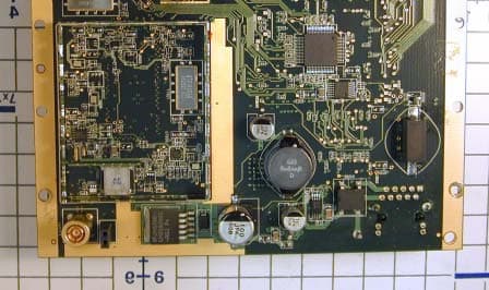
KIN915B
Sep 24, 2006Wireless Modem Module
Equipment Class
DTS - Digital Transmission System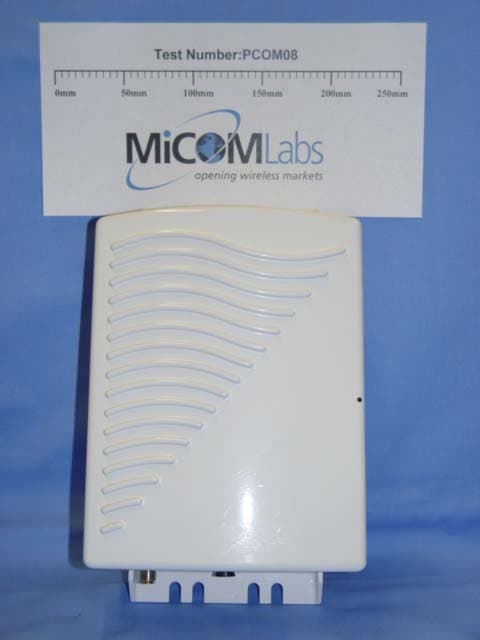
KINSL9200
Nov 16, 20052.4, 5.8 & 4.9GHz (PSB) Wireless Router
Equipment Class
DTS - Digital Transmission System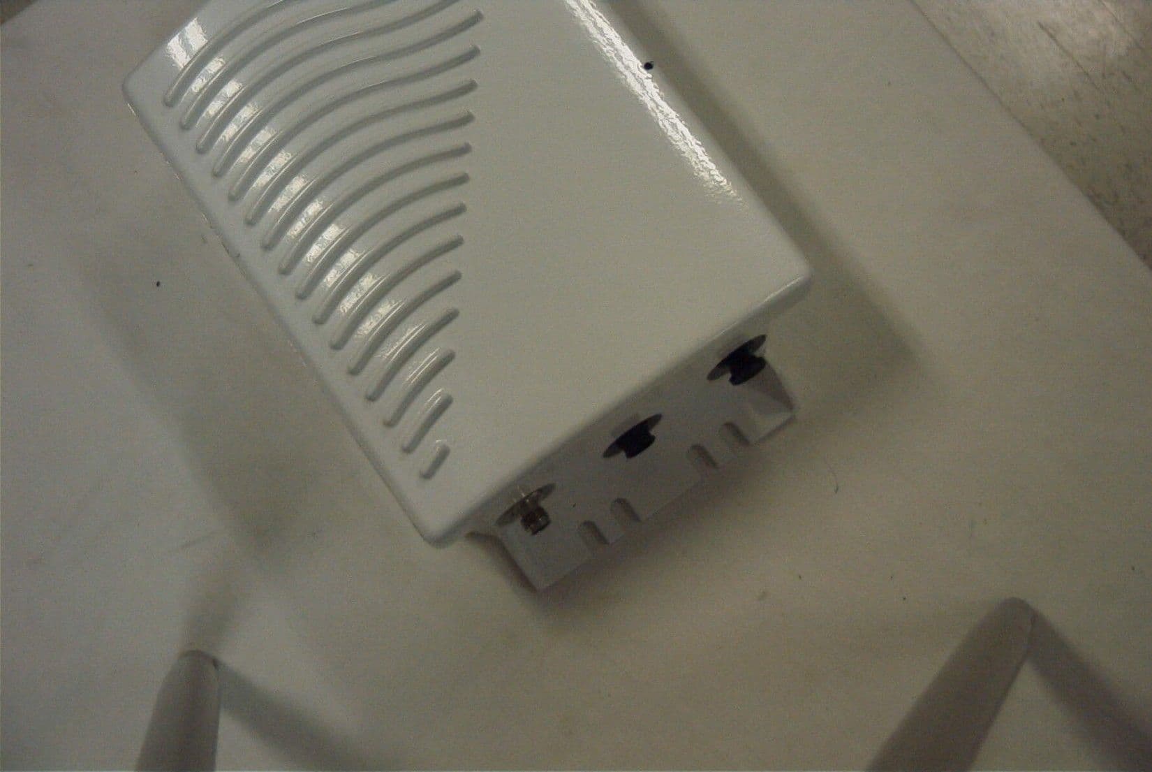
KINSL9202
Oct 11, 2004Wireless LAN
Equipment Class
DTS - Digital Transmission System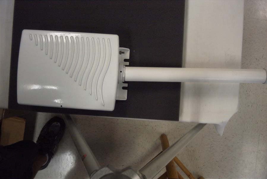
KINSL9201
Sep 28, 2004SPEEDLAN WIRELESS LAN
Equipment Class
DTS - Digital Transmission System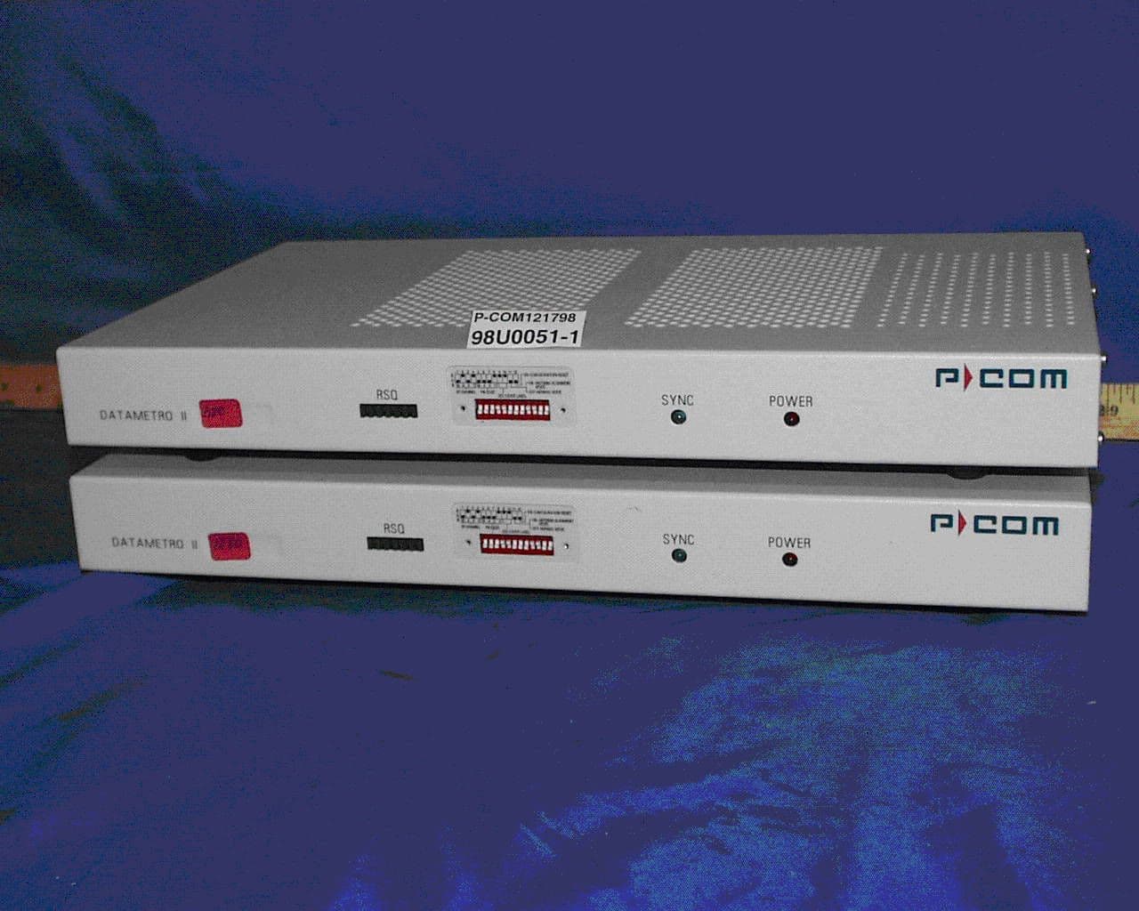
KINDM2
Mar 29, 1999Wireless Data Link
Equipment Class
DSS - Part 15 Spread Spectrum Transmitter