KINSL9201SPEEDLAN WIRELESS LAN
Wave Wireless Corporation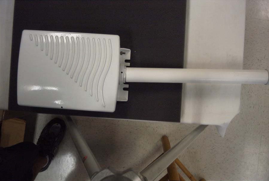
Click to zoom
Application Details
- Equipment Class
- DTS - Digital Transmission System
- Date of Grant
- Sep 28, 2004
- Application Purpose
- Original Equipment
- Date of Application
- Sep 28, 2004
- Equipment Note
- SPEEDLAN WIRELESS LAN
- Frequency Range
- 2412.00000000 - 2462.00000000
- Company
- Wave Wireless Corporation
- Country
- United States
Documents & Files
Document Text
Text extracted from the exhibit documents filed with the FCC. Open a document above to read the original.
Users Manual
SPEEDLAN 9200 User Guide Part Number 34357-MNL Rev. 03 Last Revised: 8/24/04 P-Com Copyright Statement (c) 2004. P-Com Inc. provides this Installation Guide without warranty of any kind, either express or implied, including, but not lim- ited to, the implied warranties of merchantability and fitness for a particular purpose. P-Com Inc. may make improvements and changes to the product described in this manual at any time and without any notice. P-Com Inc. assumes no respon- sibility for its use, nor any infringements of patents or other rights of third parties that would result. This publication may contain technical inaccuracies or typographical errors. Periodic changes are made to the information contained herein. These changes, and mechanical corrections, will be incorporated in subsequent revision levels of the publication. No part of this publication may be stored in a retrieval system, transmitted, or reproduced in any way, including but not limited to photocopy, photograph, magnetic or other records, without the prior written permission of P-Com Inc. All other brand and product names are the trademarks of their respective holders. P- Com Sarasota Office 7020 Professional Parkway East Sarasota, FL 34240 Technical Support 941-907-2300 (phone) 941-355-0219 (fax) SPEEDLAN 9200 User Guide Part # 34357-MNL Rev.03 Contents-1 CHAPTER 1 - Introduction Features and Benefits ................................................................................................................. 1-2 SPEEDLAN 9200 Features................................................................................................... 1-2 ISP Functionality ................................................................................................................. 1-3 IP Router Functionality ........................................................................................................1-3 Configuration Management ................................................................................................ 1-4 SPEEDManage................................................................................................................... 1-4 Features (and Benefits)........................................................................................................1-4 Priority Queuing................................................................................................................. 1-5 SNMP ............................................................................................................................... 1-6 Equipment and Hardware ................................................................................................... 1-6 SPEEDLAN 9200 Mesh Protocol -- How It Works in Mesh Cells ..................................................... 1-6 SPEEDLAN’s Mesh Cell Architecture..................................................................................... 1-8 SPEEDLAN 9200 Mesh Core Components ........................................................................... 1-9 Neighbor Discovery .................................................................................................... 1-9 Topology Updates ...................................................................................................... 1-9 Routing.................................................................................................................... 1-10 Why SPEEDLAN Outperforms Other Routing Equipment............................................... 1-10 Document Changes/Corrections ............................................................................................... 1-11 What’s New for Firmware ................................................................................................. 1-11 Contacting Technical Support ...................................................................................................1-12 CHAPTER 2- SPEEDLAN 9200 Hardware Rooftop and Tower Installations Warning ..................................................................................... 2-2 Regulatory Information ............................................................................................................... 2-2 Declaration of Conformity for RF Exposure................................................................................... 2-3 General Safety Requirements for Installation of SPEEDLAN 9200 Models........................................ 2-3 Hardware Overview ................................................................................................................... 2-4 Tips for Antenna Alignment.......................................................................................... 2-5 Drawings of Outdoor, Remote-Mounted Components .................................................................. 2-6 Indoor Junction Box............................................................................................................2-6 The SPEEDLAN 9201/9204 with an Integrated Omni-Directional........................................... 2-7 Bottom View of SPEEDLAN 9201/SPEEDLAN 9204 .............................................................. 2-8 System Description .............................................................................................................2-8 Package Contents ............................................................................................................. 2-8 Installation Steps for the SPEEDLAN 9201/SPEEDLAN 9204 .................................................. 2-9 ...................................................................................................................................... 2-10 Installation Diagram of the SPEEDLAN 9201/SPEEDLAN 9204 ............................................ 2-11 The SPEEDLAN 9202/SPEEDLAN 9203/SPEEDLAN 9205 with External Antenna ........................... 2-12 Bottom View of SPEEDLAN 9202/SPEEDLAN 9203/SPEEDLAN 9205 ................................... 2-13 …
Text truncated - open the document above for the full version.
Block Diagram
Figure 1. Block Diagram of Wireless Outdoor 2.4 GHz KINSL9201 Router To Ethernet - Cat5 Cable To 8 dBi Integrated Antenna 2.4 GHz Wireless Mini-PCI Card Junction Box Soekris net4501 Embedded Processor (CPU, Flash ROM Module, NIC Card) To Switching Power Supply 36 Vdc Voltage Regulator DC Voltage + Ethernet Cat5 Cable 12 Vdc Ethernet DC Enclosure
Operational Description
Operational Description of Wireless Outdoor Mount Ethernet Router SPEEDLAN 9201 The outdoor wireless Ethernet router, FCC ID: KINSL9201, is a high performance router that creates interconnectivity between buildings, and it is provides links for LAN-to-LAN applications. This system can be used in mesh configuration. The functional block diagram of the bridge is presented on Figure 1. The outdoor wireless Ethernet routers are installed on the pole or tower. The router containing the Atheros 2.4 GHz Transmitter / Receiver, Embedded Processor and Voltage Regulator is enclosed in a metal enclosure that is connected to the ground. The Ethernet data and DC supply voltage (36 Vdc) are injected through a junction box via a 300 ft. CAT5 Ethernet cable ( 2 pairs are used for DC voltage and other 2 for Ethernet data ), and then it is connected to the router. Then, the DC voltage is separated and connected to a Voltage Regulator, and Ethernet data are processed and transferred to an Atheros transmitter that is connected to a 8 dBi integrated omni antenna. If the system is not transmitting, it is in a receiving mode. The received signal from the antenna is amplified, processed and demodulated via CAT5 Ethernet cable connected to the LAN system. Technical Specification of SPEEDLAN 9201 Router RF INFORMATION Topologies Mesh Compatibility Full Interoperable with 2.4 GHz DSSS/OFDM Channels 2.4 GHz DSSS/OFDM: 11 Regulatory FCC Part 15 Frequency Range US/Canada-2.4 GHz DSSS/OFDM: 2.412-2.462GHz Frequency Band Spread Spectrum Signaling Rate ( Mb/s) Modulation DSSS 1 DBPSK 2 DQPSK 5.5 2.4 GHz 11 CCK OFDM 6 9 BPSK 12 18 QPSK 24 36 16 QAM 48 2.4 GHz 54 64 QAM Communication Method Half duplex Receive Sensitivity @ PER < 0.10 2.4 GHz OFDM -82 dBm @ 6 Mb/s 2.4 GHz DSSS -87 dBm @ 1 Mb/s Tx Power Tx Power Frequency 2.4GHz Specific Channels 1, 2, 10, and 11 3-9 Tx Power Supported 13 dBm (20mW) 17 dBm (50mW) Power Supply Wall unit: 100/240 VAC, 47/63Hz, 0.7A; output 24V DC, 1.0A Media Access Protocol CSMA/CA SECURITY Wireless Encryption 128 bit-AES (for 92xx) and WEP (for SPEEDMesh-enabled client) ENVIRONMENTAL Storage Temperature -40 o C to 60 o C Working Temperature -33 o C to 55 o C Start-up Temperature -20 o C to 55 o C WIRED LAN INTERFACE Compliance IEEE 802.3 Ethernet Physical Interface 10Base-T, 10/100Base-TX WIRELESS LAN INTERFACE RF Physical Interface RTNC bulkhead RF connector or integrated antenna Bit Error Rate Better than 10 -5 CONFIGURATION & MANAGEMENT Upgradeability Firmware is upgradeable via in-band management Configuration & MonitoringWeb-based, HTTPS MECHANICAL 92xx Enclosure NEMA 4 metal chassis; tower or pole-mount Dimensions (H x W x D) 9201 31.5” x 7” x 3.5” (80.0 cm x 17.8 cm x 8.9 cm) 9204 25.0” x 7” x 3.5” (63.5 cm x 17.8 cm x 8.9 cm) 9205 9” x 7” x 3.5” (22.9 cm x 17.8 cm x 8.9 cm) Weight 9201 5.5 lbs 9204 5.1 lbs 9205 4.5 lbs WARRANTY Service Warranty 1 year depot warranty, extended warranty available
Schematics
AG-621 V1.0 REVISION NUMBERINITIALSDESCRIPTION JWInitial release.245-01184-010, Rev 000 DATE 02/10/03 03/28/03245-01184-020, Rev 000VNModified Sch based on 245-01184-010 Rev.A Rework. Changed R39 to 330. Changed R89 to 150. Changed R50 to 348. Changed R51 to 200. Changed C142 to 1pF. Changed L29 to 3.3nH. Changed C143 to 1.5pF. Changed C113 to 2.2pF. Changed C110 to 3.3pF. Changed Q11 to DNI. Changed Q12 to DNI. Changed R5 to DNI. Changed R9 to 0. Changed R23 to 3.09K. Changed F8 to MDR742. Changed R63 to 28.7K. Changed C114 to 2.7pF. Changed C91 to 1pF. Removed C62, C67. Removed C81, R30, C85, C92, C89, C90, C84, L21, R37, R40. Added L41, L42 : 3.3nH. Added R107: 100, 1% ; R108: 620, 1% ; R109: 910, 1% : R105: 10 ; R106: 10. Added C346: 1uF; C347: 1uF; C348: 220pF; C350: 0.5pF. Changed U4 to LX5506. Changed F3 to DEA205425BT-2028A4. Removed R91, R62, Q9. Removed R16 ; connected L12 to 2.5V_A. Added C144: 1uF ; L43: 15uH. Changed L25 to 2.2nH. Added L44: 1.8nH. Added R112: R. 5/20/03245-01184-030, Rev 000VNAdded WoL circuit. Added BlueTooth support. Z-COM (MB32 - Mini PCI Type IIIB Card 802.11a and 802.11g Combo Radio) Mini PCI - Title Page Atheros Communications, Inc. Tuesday, August 10, 2004 15 C 529 Almanor Avenue Sunnyvale, CA 94085 001 245-01184-032 Size DWG NO RevSheetof Title Date 4.7K IRLM6401 10K 3K 2N3904 IRLM6401 STUFF ALL EXCEPT R9 FOR WAKE ON LAN. STUFF ONLY R9 TO DISABLE WAKE ON LAN. DO NOT STUFF Mini PCI - AR5212 Atheros Communications, Inc. Tuesday, August 10, 2004 25 C 529 Almanor Avenue Sunnyvale, CA 94085 001 245-01184-032 Size DWG NO RevSheetof Title Date EPRM_DI EPRM_CLK DACP_I DACN_I EPRM_CS ADCN_I AD31 PCI_GNT_L F2D2EN PCI_CLKRUN_L AD8 AD28 PCI_CBE1_L AD4 AD15 PCI_PAR PCI_PERR_L RX5 AD20 AD30 AD24 AD10 RFDATAIN PCI_INT_L PCI_RST_L ATTEN5 ATTEN2 GPIO_3 PCI_IDSEL_L PCI_DEVSEL_L AD27 PCI_REQ_L AD14 ADCRES PCI_CBE0_L PCI_SERR_L AD0 AD11 AD3 RFDATAOUT3 AD5 AD2 AD13 AD6 PCI_TRDY_L AD29 AD16 AD18 AD22 AD19 ADCP_I ADCP_Q TX5 EPRM_EN_L AD25 PCI_IRDY_L PCI_CBE2_L RX_CLEAR HITUNE5 AD17 AD12 AD9 AD1 AD23 PCI_CLK SLEEP AD21 EPRM_DO PCI_CBE3_L AD26 ADCISEL AD7 RFLOAD RFRESET_L PCI_FRAME_L RFDATAOUT1 RFDATAOUT0 DACN_Q ADCN_Q PCI_STOP_L RFSHIFT RFDATAOUT2 AR5112_CLK40_OUT LED0 LED1 TX2 GPIO_0 PCI_TRDY_L PCI_INT_L AD4 AD6 AD22 PCI_REQ_L PCI_IRDY_L AD14 PCI_PAR PCI_IDSEL_L AD13 AD9 AD10 AD3 PCI_CBE1_L AD5 AD7 PCI_CBE2_L PCI_RST_L MPCI_11MPCI_12 AD18 AD26 AD2 PCI_FRAME_L AD15 AD27 AD8 PCI_STOP_L AD1 AD19 AD21 PCI_DEVSEL_L AD31 PCI_GNT_L AD20 AD23 AD30 PCI_CLK AD12 AD28 AD16 AD11 AD25 PCI_CBE3_L PCI_CLKRUN_L AD24 PCI_SERR_L MPCI_13 PCI_CBE0_L AD0 MPCI_14 PCI_PERR_L AD29 AD17 LED1 GPIO_0 MPCI_13 MPCI_14LED0 GPIO_3 LED0 GPIO_1 MPCI_11 LED1 GPIO_2 MPCI_12 GPIO_1 GPIO_2 DACP_Q 3.3V_AUX POR_LPOR_EN HITUNE5 RX_CLEAR RX2 PCI_PME_L ANTC ANTD ADCP_Q3 ADCN_I3 ADCP_I3 RFDATAIN3 RFRESET_L3 AR5112_CLK40_OUT3 DACN_Q3 DACP_Q3 DACN_I3 RX54 RFSHIFT3 RFDATAOUT03 RFDATAOUT13 RFDATAOUT23 RFDATAOUT33 RFLOAD3 ANTA4 TX54 TX24 SLEEP5 DACP_I3 ADCN_Q3 ANTB4 ATTEN24 3.3V VCC_ADC 3.3V 3.3V VCC_CORE VCC_CORE3.3V VCC_DAC 3.3V_CON3.3V_CON3.3V3.3V 3.3V 3.3V 3.3V3.3V_CON 3.3V 3.3V 3.3V AR5212 U1 N7 K13 L14 M14 N13 N12 M11 N11 P10 P4 N3 C2 A3 N6 K14 N8 K12 L12 N14 P13 P12 D9 P11 N5 M4 A2 J1 C1 H12 B3 P2 L13 M13 M7 G3 D1 M9 P5 N4 L1 G14 J13 A4B4C4 P7 E4 D11 G4H4 E5 K4 E6 J14 D6 F14 A5B5 G12 D5 N2B13E7E8E9E10 L5M5 F12 A14 A6B6C7 F4F5F6F7F8F9F10F11C12 E1 A1 A7B7C6D7 G5G6G7G8G9G10 L7H3 B1 E13 A8B8C8D8 H5H6H7H8H9H10 L8 P3 E12 F3 A9B9C9 J4J5J6J7J8J9J10J11D4 H14 H13 A10B10C10D10 K5K6K7K8K9K10 L10M10 D3 D2 A11 B11 C11 L4 E11 L6 G11H11 L9 K11 L11 E2 E3 G13 A12 B12 M3 D12 C14 C3 P8 P9 B2 L2 K1 M12 J12 C5 A13 F2 C13 D13 N10 M6 N1 N9 M2 K3 J3 P1 F1 H2 H1 B14 E14 D14 F13 M1 M8 P6 L3 K2 J2 P14 G2 G1 PCI_TRDY_L PCI_AD1 PCI_AD3 PCI_AD6 PCI_AD9 PCI_AD11 PCI_AD13 PCI_AD14 PCI_AD16 PCI_AD19 PCI_AD22 TDO TMS PCI_FRAME_L PCI_AD0 PCI_STOP_L PCI_AD2 PCI_AD5 PCI_AD8 PCI_AD10 PCI_AD12 GND PCI_AD15 PCI_AD18 PCI_AD21 TDI PCI_CLKRUN_L TCLK SLEEP AGND PCI_SERR_L PCI_AD4 PCI_AD7 PCI_DEVSEL_L VDD2_5 RX2 PCI_IDSEL PCI_AD17 PCI_AD20 PCI_PME_L GPIO_5 ANTB ADC_QN ADC_QP AVDD_ADC PCI_CLK VDD3_3 GND VDD2_5VDD2_5 GND VDD3_3 GND ANTA GND F2D2EN AGNDAGND HITUNE5 VDD3_3 GNDGNDGNDGNDGNDGND VDD3_3VDD3_3 ANTD RFDATAOUT_0 ADC_IP ADC_IN ADCISEL GNDGNDGNDGNDGNDGNDGNDGNDGND RX5 EPRM_EN_L AGND AVDD_ADC ADCRES VDD2_5 GNDGNDGNDGNDGNDGND VDD2_5VDD2_5 TRST_L TX2 DAC_QN DAC_QP AVDD_DAC VDD2_5 GNDGNDGNDGNDGNDGND VDD2_5 PCI_RST_L TX5 RX_CLEAR AGNDAGND AVDD_DAC GNDGNDGNDGNDGNDGNDGNDGNDGND LED_1 LED_0 DAC_IP DAC_IN AVDD_PLL VDD3_3 GNDGNDGNDGNDGNDGND VDD3_3VDD3_3 GPIO_1 GPIO_0 AGND XIN XOUT GND VDD3_3 GND VDD2_5VDD2_5 GND VDD3_3 GND GPIO_2 GPIO_3 GPIO_4 RFRESET_L RFLOAD GND ANTC RFDATAOUT_3 GND PCI_INT_L PCI_PERR_L GND PCI_AD26 PCI_AD29 GND ATTEN2 PCI_MODE RFSHIFT EPRM_DO RFDATAOUT_2 RFDATAIN5 PCI_CBE1_L PCI_CBE2_L PCI_REQ_L PCI_PAR PCI_AD24 PCI_AD27 PCI_AD30 PCI_AD23 EPRM_DI ATTEN5 EPRM_CLK RFDATAOUT_1 PLLBYPASS REFCLK CLKOBS PCI_CBE3_L PCI_GNT_L PCI_IRDY_L PCI_AD25 PCI_AD28 PCI_AD31 PCI_CBE0_L RFDATAIN2 EPRM_CS R R8 J1 Mini PCI -Type III 12 34 56 78 910 1112 1314 1516 1718 1920 2122 2324 2526 2728 2930 3132 3334 3536 3738 3940 4142 4344 4546 4748 4950 5152 5354 5556 5758 5960 6162 6364 6566 6768 6970 7172 7374 7576 7778 7980 8182 8384 8586 8788 8990 9192 9394 9596 9798 99100 101102 103104 105106 107108 109110 111112 113114 115116 117118 119120 121122 123124 TIPRING 8PMJ-38PMJ-1 8PMJ-68PMJ-2 8PMJ-78PMJ-4 8PMJ-88PMJ-5 LED1-GRNPLED2-YELP LED1-GRNNLED2-YELN CHSGNDRESERVED1 INTB#5V 3.3VINTA# RESERVED2RESERVED3 GND3.3VAUX CLKRST# GND3.3V REQ#GNT# 3.3VGND AD31PME# AD29RESERVED4 GNDAD30 AD273.3V AD25AD28 RESERVED5AD26 CBE3#AD24 AD23IDSEL GNDGND AD21AD22 AD19AD20 GNDPAR AD17AD18 CBE2#AD16 IRDY#GND 3.3VFRAME# CLKRUN#TRDY# SERR#STOP# GND3.3V PERR#DEVSEL# CBE1#GND AD14AD15 GNDAD13 AD12AD11 AD10GND GNDAD9 AD8CBE0# AD73.3V 3.3VAD6 AD5AD4 RESERVED6AD2 AD3AD0 5VRESERVED-WIP1 AD1RESERVED-WIP2 GNDGND AC_SYNCM66EN AC_SDATA_INAC_SDATA_OUT AC_BIT_CLKAC_CODEC_ID0# AC_CODEC_ID1#AC_RESET# MOD_AUDI…
Text truncated - open the document above for the full version.
Test Report
TIMCO ENGINEERING INC. 849 NW State Road 45 Newberry, Florida 32669 http://www.timcoengr.com 888.472.2424 F 352.472.2030 email: [email protected] APPLICANT: P-COM, INC FCC ID: Test Report Product Name: ROUTER FCC ID: KINSL9201 Applicant: P-COM, INC. 7020 PROFESSIONAL PARKWAY EAST SARASOTA FL 34240-8415 Date Receipt: AUGUST 25, 2004 Date Tested: SEPTEMBER 22, 2004 KINSL9201 REPORT #: P\P-COM_KIN\1378UT4\1378UT4TestReport.doc COVER PAGE TIMCO ENGINEERING INC. 849 NW State Road 45 Newberry, Florida 32669 http://www.timcoengr.com 888.472.2424 F 352.472.2030 email: [email protected] APPLICANT: P-COM, INC FCC ID: TABLE OF CONTENTS TEST REPORT CONTAINING: PAGE 1.............LETTER OF EXPLANATION PAGE 2.............LIST OF TEST EQUIPMENT PAGE 3.............TEST PROCEDURES PAGE 4.............POWERLINE CONDUCTED INTERFERENCE PAGE 5-6...........POWERLINE CONDUCTED PLOTS PAGE 7.............RADIATION INTERFERENCE TEST DATA PAGE 9.............6 dB BANDWIDTH PLOTS PAGE 10............POWER OUTPUT PAGE 11-12.........SPURIOUS EMISSIONS AT ANTENNA TERMINALS DATA PAGE 13............METHOD OF MEASURING RF CONDUCTED PAGE 14-15.........FIELD STRENGTH OF SPURIOUS EMISSIONS PAGE 16............METHOD OF MEASURING RADIATED SPURIOUS EMISSIONS PAGE 17-25.........RADIATED SPURIOUS EMISSIONS INTO ADJACENT RESTRICTED BANDS PAGE 26-27.........POWER SPECTRAL DENSITY EXHIBITS INCLUDED: REQUEST FOR CONFIDENTIALITY LETTER BLOCK DIAGRAM SCHEMATICS USERS MANUAL LABEL SAMPLE LABEL LOCATION EXTERNAL PHOTOGRAPHS INTERNAL PHOTOGRAPHS OPERATIONAL DESCRIPTION TEST SET UP PHOTOGRAPHS KINSL9201 REPORT #: P\P-COM_KIN\1378UT4\1378UT4TestReport.doc TABLE OF CONTENTS TIMCO ENGINEERING INC. 849 NW State Road 45 Newberry, Florida 32669 http://www.timcoengr.com 888.472.2424 F 352.472.2030 email: [email protected] APPLICANT: P-COM, INC FCC ID: SEPTEMBER 22, 2004 Federal Communications Commission Authorization and Evaluation Division 7435 Oakland Mills Road Columbia, MD 21046 SUBJECT: P-COM, INC. FCC ID: KINSL9201 To Whom It May Concern: The attached report is for a wireless lan device with both DSSS and OFDM modulations. The device operates only in the 2.4 GHz ISM band. The assembly, made up of the Bridge/Radio (FCC ID:KINSL9201, 50 to 300 feet of special ethernet/power cable, and an integrated 8 dBi omni antenna. P-Com sells only professionally installed equipment. This unit has output power control via software and is not user selectable or accessible. The following table shows the power output verses channel availability. 9201 2.4 GHz OFDM 1, 2, 10, & 118 dBi omni 22 mW 13.4 dBm 9201 2.4 DSSS 1, 2, 10, & 118 dBi omni 26 14.2 9201 2.4 OFDM 3 through 9 8 dBi omni 50 17.0 9201 2.4 DSSS 3 through 9 8 dBi omni 50 17.0 P-COM, INC. purchases a standard antenna from the manufacturer. The antenna is intended to be used outside. Should you have any questions or require any further information with regards to this, please feel free to contact me. Sincerely, Mario R. de Aranzeta C.E.T. MRD/sh Encl. KINSL9201 REPORT #: P\P-COM_KIN\1378UT4\1378UT4TestReport.doc Page 1 of 27 TIMCO ENGINEERING INC. 849 NW State Road 45 Newberry, Florida 32669 http://www.timcoengr.com 888.472.2424 F 352.472.2030 email: [email protected] APPLICANT: P-COM, INC FCC ID: EMC Equipment List Device ManufacturerModel Serial Number Cal/Char Date 3/10-Meter OATS TEI N/A N/A Listed 3/27/04 3-Meter OATS TEI N/A N/A Listed 1/13/03 Biconnical Antenna Eaton 94455-1 1057 CAL 3/18/03 Biconnical Antenna Eaton 94455-1 1096 CAL 10/1/01 Biconnical Antenna Electro- Metrics BIA-25 1171 CAL 4/26/01 Double- Ridged Horn Antenna Electro- Metrics RGA-180 2319 CAL 2/17/03 LISN Electro- Metrics ANS-25/2 2604 CAL 10/9/01 LISN Electro- Metrics EM-7820 2682 CAL 3/12/03 Log- Periodic Antenna Eaton 96005 1243 CAL 5/8/03 KINSL9201 REPORT #: P\P-COM_KIN\1378UT4\1378UT4TestReport.doc Page 2 of 27 TIMCO ENGINEERING INC. 849 NW State Road 45 Newberry, Florida 32669 http://www.timcoengr.com 888.472.2424 F 352.472.2030 email: [email protected] APPLICANT: P-COM, INC FCC ID: TEST PROCEDURE GENERAL: This report shall NOT be reproduced except in full without the written approval of TIMCO ENGINEERING, INC. POWER LINE CONDUCTED INTERFERENCE: The procedure used was ANSI STANDARD C63.4- 1992 using a 50uH LISN. Both lines were observed with the UUT transmitting. The bandwidth of the spectrum analyzer was 10kHz with an appropriate sweep speed. The ambient temperature of the UUT was 76°F with a humidity of 55%. BANDWIDTH 6.0dB: The measurements were made with the spectrum analyzer's resolution bandwidth (RBW)=1 MHz and the video bandwidth (VBW) =3 MHz and the span set as shown on plot. POWER OUTPUT: The RF power output was measured at the antenna feed point using a peak power meter. ANTENNA CONDUCTED EMISSIONS: The RBW=100 kHz, VBW=300 kHz and the span set to 10 MHz and the spectrum was scanned from 30 MHz to the 10 th Harmonic of the fundamental. Above 1GHz the resolution bandwidth was 1 MHz and the VBW =3 MHz and the span to 50 MHz. RADIATION INTERFERENCE: The test procedure used was ANSI STANDARD C63.4-2000 using a Agilent spectrum analyzer with a pre-selector. The bandwidth (RBW) of the spectrum analyzer was 100 kHz up to 1 GHz and 1 MHz above 1 GHz with an appropriate sweep speed. The VBW above 1 GHz was = 3 MHz. The analyzer was calibrated in dB above a micro volt at the output of the antenna. The ambient temperature of the UUT was 76°F with a humidity of 55%. KINSL9201 REPORT #: P\P-COM_KIN\1378UT4\1378UT4TestReport.doc Page 3 of 27 TIMCO ENGINEERING INC. 849 NW State Road 45 Newberry, Florida 32669 http://www.timcoengr.com 888.472.2424 F 352.472.2030 email: [email protected] APPLICANT: P-COM, INC FCC ID: APPLICANT: P-COM, INC. FCC ID: KINSL9201 NAME OF TEST: POWER LINE CONDUCTED INTERFERENCE RULES PART NO.: 15.207(a) REQUIREMENTS: QUASI-PEAK AVERAGE .15 – 0.5 MHz 66-56 dBuV 56-46 dBuV 0.5 – 5.0 56 46 5.0 – 30. 60 50 TEST PROCEDURE: ANSI STANDARD C63.4-2000. The spectrum was scanned from 0.15 to 30 MHz. TEST DATA: TH…
Text truncated - open the document above for the full version.
Test Setup Photos
RADIATED TEST SET UP PHOTO POWERLINE CONDUCTED TEST SET UP PHOTO
Contact Information
Applicant
Carl Lynch
Test Firm
Timco Engineering, Inc.S Sanders
Technical Specifications
| # | Rule Parts | Frequency Range | Power Output |
|---|---|---|---|
| 1 | 15C | 2.41 GHz - 2.46 GHz | 50.00 mW |
Other Applications from Wave Wireless Corporation
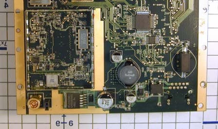
KIN915B
Sep 24, 2006Wireless Modem Module
Equipment Class
DTS - Digital Transmission System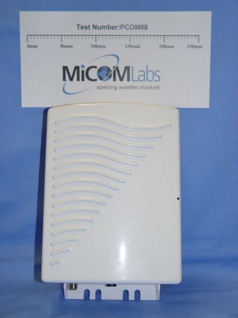
KINSL9200
Nov 16, 20052.4, 5.8 & 4.9GHz (PSB) Wireless Router
Equipment Class
DTS - Digital Transmission System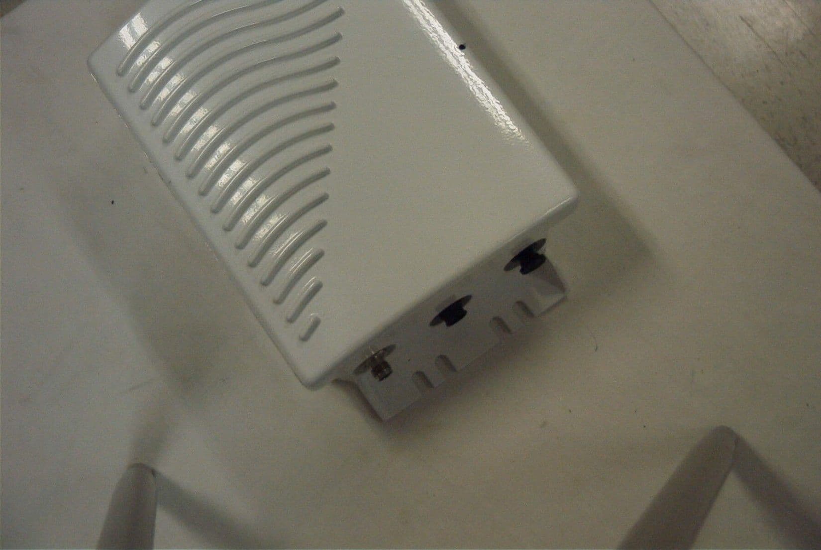
KINSL9202
Oct 11, 2004Wireless LAN
Equipment Class
DTS - Digital Transmission System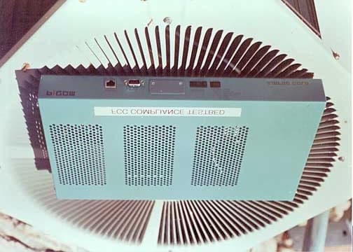
KINAPG20FNET
Mar 13, 2002Wireless LAN, AIRPRO GOLD 20F.NET
Equipment Class
DSS - Part 15 Spread Spectrum Transmitter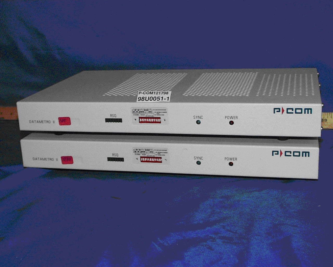
KINDM2
Mar 29, 1999Wireless Data Link
Equipment Class
DSS - Part 15 Spread Spectrum Transmitter