KRE50A25 - 50 MHz Base Station Transceiver
RF Technology Pty Ltd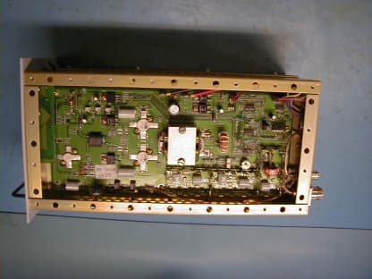
Click to zoom
Application Details
- Equipment Class
- TNB - Licensed Non-Broadcast Station Transmitter
- Date of Grant
- May 08, 2002
- Application Purpose
- Original Equipment
- Date of Application
- Mar 17, 2002
- Equipment Note
- 25 - 50 MHz Base Station Transceiver
- Frequency Range
- 25.00000000 - 50.00000000
- Company
- RF Technology Pty Ltd
- Country
- Australia
Documents & Files
Document Text
Text extracted from the exhibit documents filed with the FCC. Open a document above to read the original.
Users Manual
Eclipse Series RF Technology [email protected] November, 2001 R50 Receiver Operation and Maintenance Manual This manual is produced by RF Technology Pty Ltd 10/8 Leighton Place, Hornsby NSW 2077 Australia Copyright © 2001 RF Technology Page 2RF Technology R50 CONTENTSCONTENTS Contents 1Operating Instructions 1 1.1Front Panel Controls4 1.1.1MON. Volume4 1.1.2MON. SQ4 1.1.3N. SQ4 1.1.4C. SQ5 1.1.5LINE5 1.2 Front Panel Indicators5 1.2.1PER LED5 1.2.2SQ LED6 1.2.3ALARM LED6 2Receiver Options6 2.1Serial I/O Parameters6 2.2Receiver Low Battery Level7 2.3Audio High Pass (Notch) Filter7 2.4Audio Response7 2.5LOOP VOLTS Select7 2.6CO S P olarity Select7 2.7COS Source/Sink Select7 2.8Channel Selectable Parameters7 3Receiver I/O Connections8 3.125 Pin Connector8 3.29 Pin Front Panel Connector9 4Channel Programming and Option Settings9 4.1Setting Options9 4.2Setting Channel Parameters10 5Circuit Description 5.1R50 Master Schematic (Sheet 1)11 5.2Microprocessor (Sheet 2)12 5.3RF Section (Sheet 3)14 5.4Receiver Section (Sheet 4)15 5.5Voltage Controlled Oscillator (Sheet 5)16 5.6Audio Processing Section (Sheet 6)16 5.7Power Generation Section (Sheet 7)17 6Field Alignment (Calibration) Procedure 18 6.1Standard Test Equipment18 6.2Invoking the Calibration Procedure18 6.3The "Miscellaneous" Calibration Procedure19 6.4The "Line" Calibration Procedure20 6.5The "Reference" Calibration Procedure20 7Specifications 21 7.1Overall Description 21 7.1.1Channel Capacity21 RF Technology R50Page 3 CONTENTSCONTENTS 7.1.2CTCSS21 7.1.3Channel Programming21 7.1.4Channel Selection21 7.1.5Microprocessor22 7.2Physical Configuration22 7.3Front Panel Controls, Indicators and Test Points22 7.3.1Controls22 7.3.2Indicators22 7.3.3Test Points22 7.4Electrical Specifications23 7.4.1Power Requirements23 7.4.2Frequency Range and Channel Spacing23 7.4.3Frequency Synthesizer Step Size23 7.4.4Frequency Stability23 7.4.5Number of Channels23 7.4.6RF Input Impedance23 7.4.7IF Frequencies23 7.4.8Sensitivity24 7.4.9Selectivity24 7.4.10 Spurious and Image Rejection24 7.4.11 Intermodulation24 7.4.12 Modulation Acceptance BW24 7.4.13 Noise Squelch24 7.4.14 Carrier Level Squelch24 7.4.15 Receiver Frequency Spread24 7.4.16 Receiver Conductive Spurious25 7.4.17 Audio Frequency Response25 7.4.18 Audio Output Level25 7.4.19 Audio Distortion25 7.4.20 Channel Select Input / Output25 7.4.21 Carrier Operated Switch Output26 7.4.22 Current Source/Sink, Collector Voltage 26 7.4.23 CTCSS26 7.4.24 External Squelch Input26 7.5Connectors26 7.5.1Antenna Connector26 7.5.2Power and I/O Connector26 7.5.3Test Connector27 Appendix AEIA CTCSS Tone Frequencies28 Appendix CParts List29 Appendix CEngineering Diagrams C.1 Block Diagram C.2 Circuit Diagra ms C.3 Component Overlay Diagrams Page 4RF Technology R50 1 OPERATING INSTRUCTIONS 1Operating Instructions 1.1 Front Panel Controls 1.1.1MON. Volume The Mon. Volume control is used to adjust the volume of the internal loudspeaker and any external speaker connected to the test socket. It does not effect the level of the 600 Ohm line or direct audio output. 1.1.2MON.SQ The MON. SQ. switch allows the normal squelch functions controlling the monitor output to be disabled. When the switch is in the MON. SQ. position the audio at the monitor speaker is controlled by the noise detector. The CTCSS, carrier and external squelch functions are disabled. This can be useful when you are trying to trace the source of on channel interference or when setting the noise squelch threshold. The audio from the 600 Ohm line and direct outputs is not effected by the switch position. 1.1.3N.SQ The N.SQ trimpot is used to set the noise squelch sensitivity. Use the following procedure to set the noise squelch to maximum sensitivity. (a) Set the toggle switch to the MON.SQ. position and set the MON VOLUME control to 9 o'clock. (b) Turn the N.SQ. adjustment counter clockwise until the squelch opens and noise is heard from the speaker. Adjust the VOLUME to a comfortable listening level. WARNING Changes or modifications not expressly approved by RF Technology could void your authority to operate this equipment. Specifications may vary from those given in this document in accordance with requirements of local authorities. RF Technology equipment is subject to continual improvement and RF Technology reserves the right to change performance and specification without further notice. RF Technology R50Page 5 1 OPERATING INSTRUCTIONS 1.1.4 C. SQ (c) In the absence of any on channel signal, Turn the N.SQ. screw clockwise until the until the noise in the speaker is muted. Then turn the screw two additional turns in the clockwise direction. 1.1.4C.SQ The C.SQ trimpot is used to set the carrier squelch sensitivity. Carrier squelch is useful at higher signal levels than noise squelch and can be used from 1 - 200 uV input. It is provided mainly for use in fixed link applications where a high minimum signal to noise ratio is required or where very fast squelch operation is required for data transmission. The carrier squelch will open and close in less than 2 mSec. In most base station applications carrier squelch is disabled by turning the adjustment counter clockwise until the screw clicks. The carrier squelch may be set to a predetermined level with the TecHelp software or by using the following procedure: (a) First turn the adjustment fully counter-clockwise. Then set the noise squelch as above. (b) Connect a source of an on channel signal with the desired threshold level to the receiver's RF input. (c) Turn the screw clockwise until the SQ LED goes OFF. Then turn the screw back until the LED just comes ON. 1.1.5LINE The LINE trimpot is used to set the line and direct audio output level. It is normally set to give 0 dBm ( 775 mV ) to line with a standard input signal equal to 60% of maximum deviation at 1 KHz. The level can be measured between test socket pins 6 & 1 and set as desired. 1.2 Front Panel Indicators 1.2.1PWR LED The PWR LED shows that the …
Text truncated - open the document above for the full version.
Users Manual
Eclipse Series RF Technology [email protected] November, 2001 PA50 Amplifier Operation and Maintenance Manual This manual is produced by RF Technology Pty Ltd 10/8 Leighton Place, Hornsby 2077 Australia Copyright © 2001, RF Technology Page 2RF Technology PA50 CONTENTSCONTENTS Contents 1Operating Instructions3 1.2Front Panel Indicators3 2Internal Adjustments3 3Test Points4 4I/O Connections4 5Circuit Description5 5.1Driver Stage5 5.2Output Stage5 5.3Low Pass Filter5 5.4Bias Supply5 5.5Reflectometer6 5.6Metering Circuits6 6Specifications7 6.1Physical Configuration7 6.2Indicators and Test Points7 6.3Electrical Specifications7 6.3.1Power Requirements7 RF Technology PA50Page 3 1 OPERATING INSTRUCTIONS 1Operating Instructions The PA50 is part of the Eclipse range of modular base station equipment. It is a power amplifier capable of delivering 120 Watts in the VHF frequency range. It is designed to complement the T50 transmitter, and mounts in a standard Eclipse sub-rack. 1.2 Front Panel Indicators PWR LED Power LED indicates that the PA50 is connected to a DC power source. RFO LED RF Output LED indicates that the PA50 is being driven by the exciter and RF Output is available at the antenna socket. TEMP LED Temperature LED indicates that the output transistors are above 90 degrees. This is only an indication and not an alarm condition as the exciter monitors the PA50 temperature at all times in order to keep within safe operating limits. 2Internal Adjustments All internal adjustments are factory set and should not need to be changed under normal conditions. R238Driver bias adjustment R239O/P Q101 bias adjustment R240O/P Q100 bias adjustment R227Forward power meter adjustment R228Reverse power meter adjustment C209Reflectometer balance adjustment WARNING Changes or modifications not expressly approved by RF Technology could void your authority to operate this equipment. Specifications may vary from those given in this document in accordance with requirements of local authorities. RF Technology equipment is subject to continual improvement and RF Technology reserves the right to change performance and specification without further notice. Page 4RF Technology PA50 3 TEST POINTS 3Test Points These test points are provided on the PCB and the DB9 front panel connector for use by maintenance personnel TP100 and TP101Driver drain current measurement. A multimeter placed across these pins will indicate 1 volt for 1 amp of Q102 drain current TP102 and TP103O/P stage drain current measurement. A multimeter placed across these pins will indicate 1 volt for 10 amps of Q100 and Q101 drain current TP200PA Temperature reading. 1 volt indicates a temperature of 40 degrees. This reading deviates by 10mV per degree of change TP203Reverse voltage output from the reflectometer TP204Forward voltage output from the reflectometer DB9 pin 1GND DB9 pin 2O/P drain current DB9 pin 3 DB9 pin 4Reverse voltage DB9 pin 5+28V DB9 pin 6Driver drain current DB9 pin 7 DB9 pin 8Forward voltage DB9 pin 9 4I/O Connections There are 3 I/O connectors on the rear panel with the following functions 25 pin connectorDC power and exciter logic interface Pin 1,2,3,4,14,15,16,17GND Pin 10,11,12,13,22,23,24,15+28V Pin 7DATA-IO Pin 19CLK Pin 20CS Pin 18VREFB Pin 6Forward Volts Pin 8Reverse Volts Pin 9Temperature BNC Connector:RF Input from exciter, approximately1 Watt N Connector:RF Output to antenna, up to 150 Watts RF Technology PA50Page 5 5 CIRCUIT DESCRIPTION 5Circuit Description The following descriptions should be read as an aid to understanding the block and schematic diagrams. 5.1Driver Stage The function of the driver stage is to transform the RF input signal from the exciter to the appropriate levels and impedance required by the output stage. The RF input signal is applied to the high pass filter ( C121, C130, C131, C132, C133, L102 and L106 ). This filter suppresses any residual low frequency spurious that may be present at the exciter output. T100 is used to transform the nominal 50 ohm output from the exciter to match the input of Q102. A negative feedback network ( C120, R130, R132, R131, R133, R125, R129, L107 and R124 ) is used to achieve a reasonably flat gain across the frequency of operation and to match the drive level requirements of the PA50 to the output level provided by the exciter. DC bias is applied to the gate of Q102 via R120 and R121 and is decoupled by C106 and C116. The DC feed for Q102 drain is decoupled by L100, C112, C102, C100 and C118. T101 is used for impedance matching between the driver and output stage and to provide a balanced feed for the push-pull output stage 5.2 Output Stage The output stage amplifies the 5 – 10 W from the driver to in excess of 150 W for final delivery into the low pass filter. Q100 and 101 are driven in push-pull configuration by the outputs of T101. L105, R126, C126 and L104, R127, C127 form negative feedback paths in order to achieve a reasonably flat frequency response across the frequency of operation. T102 is used to provide the DC feed via the centre tap in the primary winding to Q100 and Q101. T102 also combines the balanced output of the transistors into a single ended output as well as provide the necessary impedance transformation from the transistors into a nominal 50 ohms. A small DC bias is applied to the gates of Q100 and Q102 via R118, 119, 122 and 123 and decoupled by C103, 113, 107 and 117. The DC feed to the transformer is decoupled by L103, L101, C101, 119, 104, 114, 105, 115 and 128. 5.3 Low Pass Filter The low pass filter attenuates spurious emissions to less than –86dBc. 5.4 Bias Supply The function of the bias supplies is to provide a temperature compensated bias voltage to the gates of Q100, Q101 and Q102 for adjustment to their quiescent currents. U205 and R213, R214 and R215 provide the bias voltages. U200D provides a decreasing output voltage with increasing temperature. The resistive dividers R214, R229 and Page 6RF Technology PA50 5 CIRCUIT D…
Text truncated - open the document above for the full version.
Users Manual
Eclipse Series RF Technology [email protected] November, 2001 T50 Transmitter Operation and Maintenance Manual This manual is produced by RF Technology Pty Ltd 10/8 Leighton Place, Hornsby NSW 2077 Australia Copyright © 2001 RF Technology Page 2RF Technology T50 CONTENTS CONTENTS Contents 1Operating Instructions5 1.1Front Panel Controls and Indicators5 1.1.1PTT5 1.1.2Line5 1.1.3POWER LED6 1.1.4TX LED6 1.1.5ALARM LED6 2 Transmitter Internal Jumper Options7 2.1Serial I/O Parameters7 2.2Line Terminators7 2.3Exciter Low Battery Level7 2.4External PA Parameters7 2.5LOOP Volts Select7 2.6Direct Audio (TONE) Select8 2.7Direct Audio (TONE) High Pass Filter Select8 2.8Transmit Time8 2.9Channel Selectable Parameters8 3Transmitter I/O Connections8 3.125 Pin Connector8 3.29 Pin Front Panel Connector9 4Channel and Tone Frequency Programming10 4.1Setting Options10 4.2Setting Channel Parameters11 5Circuit Description13 5.1T50 Master Schematic (Sheet 1)13 5.2Microprocessor (Sheet 2)13 5.3Audio Processing Section (Sheet 3)13 5.4Line Input Processing Section (Sheet 4)13 5.5Tone Generation Section (Sheet 5)20 5.6Frequency Synthesiser (Sheet 6)21 5.6.1The Modulation PLL21 5.6.2The Channel PLL22 5.6.3The External Reference Divider23 5.6.4The DAC23 5.6.5The VCOs and the RF Output24 5.7Voltage Controlled Oscillators (Sheet 7)24 5.81W Broadband HF Power Amplifier (Sheet 8)26 5.9Power Generation Section (Sheet 9)26 6Field Alignment Procedure27 6.1Standard Test Equipment27 6.2Invoking the Calibration Procedure28 6.3The “Miscellaneous” Calibration Procedure28 6.4The “Reference” Calibration Procedure29 RF Technology T50Page 3 CONTENTS CONTENTS 6.5The “Deviation” Calibration Procedure31 6.6The “Tone Deviation” Calibration Procedure32 6.7The “Line” Calibration Procedure33 6.8The “Power” Calibration Procedure34 7Specifications36 7.1Overall Description36 7.1.1Channel Capacity36 7.1.2CTCSS37 7.1.3Channel Programming37 7.1.4Channel Selection37 7.1.5Microprocessor38 7.2Physical Configuration38 7.3Front Panel Controls, Indicators and Test Points38 7.3.1Controls38 7.3.2Indicators38 7.3.3Test Points38 7.4 Electrical Specifications38 7.4.1Power Requirements38 7.4.2Frequency Range and Channel Spacing39 7.4.3Frequency Synthesizer Step Size39 7.4.4Frequency Stability39 7.4.5Number of Channels39 7.4.6Antenna Impedance39 7.4.7Output Power39 7.4.8Transmit Duty Cycle39 7.4.9Spurious and Harmonics39 7.4.10Carrier and Modulation Attack Time40 7.4.11Modulation40 7.4.12Distortion40 7.4.13Residual Modulation and Noise40 7.4.14600 Ω Line Input Sensitivity40 7.4.15Test Microphone Input40 7.4.16External Tone Input40 7.4.17T/R Relay Driver40 7.4.18Channel Select Input / Output41 7.4.19DC Remote Keying41 7.4.20PTT in41 7.4.21Programmable No-Tone Period41 7.4.22Firmware Timers41 7.4.23CTCSS42 7.5Connectors42 7.5.1RF Output Connector42 7.5.2Power and I/O Connector42 7.5.3External Reference Connector (optional)42 Page 4RF Technology T50 1. CONTENTS CONTENTS AEngineering Diagrams43 A.1Block Diagram43 A.2Circuit Diagra ms43 A.3Component Overlay Diagrams43 BParts List44 CEIA CTCSS Tones60 RF Technology T50Page 5 1OPERATING INSTRUCTIONS 1Operating Instructions 1.1Front Panel Controls and Indicators 1.1.1PTT A front-panel push-to-talk (PTT) button is provided to facilitate bench and field tests and adjustments. The button is a momentary action type. When keyed, audio from the line input is disabled so that a carrier with subtone is transmitted. The front-panel microphone input is not enabled in this mode, but it is enabled when the PTT line on that socket is pulled to ground. The PTT button has another function when transmission is keyed up, and the TX LED light is showing. If there is a “forward power low” alarm (the ALARM LED flashes three times, then pauses), pressing this will cause the ALARM LED to flash 6, 7, 8, or 9 times before the pause (see Table 2). This will indicate what has caused the low power alarm. 1.1.2Line The LINE trimpot is accessible by means of a small screwdriver from the front panel of the module. It is used to set the correct sensitivity of either line input or the direct audio input. It is factory preset to give 60% of rated deviation with an input of 0dBm (1mW on 600 Ω equivalent to 775mV RMS or about 2.2V peak-to-peak) at 1kHz. The nominal 60% deviation level may be adjusted by measuring between pins 6 and 1 on the test socket, and adjusting the pot. By this means an input sensitivity from approximately -12dBm to +12dBm may be established. An internal, software selectable, option, provides an extra gain step of 20dB. This, effectively changes the input sensitivity to –32 to –8dBm. WARNING Changes or modifications not expressly approved by RF Technology could void your authority to operate this equipment. Specifications may vary from those given in this document in accordance with requirements of local authorities. RF Technology equipment is subject to continual improvement and RF Technology reserves the right to change performance and specification without further notice. Page 6RF Technology T50 1.1.3Power Led 1 OPERATING INSTRUCTIONS LED Flash CadenceFault Condition 9 flashes, pauseExternal PA failure 8 flashes, pauseLow dc supply on External PA 7 flashes, pauseExternal PA Over Current Condition 6 flashes, pauseExternal PA Over Temperature 5 flashes, pauseSynthesizer unlocked 3 flashes, pauseUnable to communicate with External PA 2 flashes, pauseThe current channel is not programmed or the frequency is out of range. 1 flash, pauseLow dc supply voltage LED ON continuouslyTransmitter timed out Table 1: Interpretations of LED flash cadence (TX LED Off) LED Flash CadenceFault Condition 9 flashes, pauseExternal PA failure (if PTT is pressed) 8 flashes, pauseLow dc supply on External PA (if PTT is pressed) 7 flashes, pauseExternal PA Over Current Condition(if PTT is pressed) 6 flashes, pauseExternal PA Over Temperature(if PTT is pressed) 4 flashes, pauseEither PLL is near operational limit 3 flashes, pauseForward Powe…
Text truncated - open the document above for the full version.
Attestation Statements
EMC Technologies (NZ) Ltd Test Report No 20308 FCC Report date: 18 March 2002 EMC Techno lo gies (NZ) Ltd Telephone: +64 9 360 0862 Fax: +64 9 360 0861 STREET ADDRESS - 47 MacKelvie Street, Grey Lynn, Auckland, New Zealand E-mail: [email protected] POSTAL ADDRESS - PO Box 68 307, Newton, Auckland, New ZealandWeb Site: www.emctech.com.au This report may not be reproduced except in full 6. ATTESTATION This report describes the tests and measurements performed for the purpose of determining compliance with the specification with the following conditions: The client selected the test sample. The report relates only to the sample tested. This report does not contain corrections or erasures. Measurement uncertainties with statistical confidence intervals of 95% are shown below test results. Both Class A and Class B uncertainties have been accounted for, as well as influence uncertainties where appropriate. In addition this equipment has been tested in accordance with the requirements contained in the appropriate Commission re gulations. To the best of my knowledge, these tests were performed using measurement procedures that are consistent with industry or Commission standards and demonstrate that the equipment complies with the appropriate standards. I further certify that the necessary measurements were made by EMC Technologies NZ Ltd, 47 MacKelvie Street, Grey Lynn, Auckland, New Zealand. Andrew Cutler General Manager EMC Technologies NZ Ltd
External Photos
RF Technologies Pty Ltd – Power Amplifier Photographs. PA50A PA50B PA50C
ID Label/Location Info
R F Technology Pty. Ltd. Sydney, Australia Model No.R50 FCC IDKRE50A Serial No.00101 R F Technology Pty. Ltd. Sydney, Australia Model No.T50 FCC IDKRE50A Serial No.00101 R F Technology Pty. Ltd. Sydney, Australia Model No.PA50A FCC IDKRE50A Serial No.00101 R F Technology Pty. Ltd. Sydney, Australia Model No.PA50B FCC IDKRE50A Serial No.00101 R F Technology Pty. Ltd. Sydney, Australia Model No.PA50C FCC IDKRE50A Serial No.00101 ECLIPSE 50 Series labels
Internal Photos
EMC Technologies (NZ) Ltd Test Report No 20308 FCC Report date: 18 March 2002 EM C Te chnolog ie s (NZ) Lt d Telephone: +64 9 360 0862 Fax: +64 9 360 0861 STREET ADDRESS - 47 MacKelvie Street, Gre y Lynn, Auck la nd, New Zea la ndE- ma il: aucklab@ ihug.co.nz POSTAL ADDRESS - PO Box 68 307, Newton, Auckland, New ZealandWeb Site: www.emctech.com.au T his re po rt may not be re produce d e xce pt i n f ull 10. PHOTOGRAPH (S) Receiver EMC Technologies (NZ) Ltd Test Report No 20308 FCC Report date: 18 March 2002 EM C Te chnolog ie s (NZ) Lt d Telephone: +64 9 360 0862 Fax: +64 9 360 0861 STREET ADDRESS - 47 MacKelvie Street, Gre y Lynn, Auck la nd, New Zea la ndE- ma il: aucklab@ ihug.co.nz POSTAL ADDRESS - PO Box 68 307, Newton, Auckland, New ZealandWeb Site: www.emctech.com.au T his re po rt may not be re produce d e xce pt i n f ull Transmitter / Exciter EMC Technologies (NZ) Ltd Test Report No 20308 FCC Report date: 18 March 2002 EM C Te chnolog ie s (NZ) Lt d Telephone: +64 9 360 0862 Fax: +64 9 360 0861 STREET ADDRESS - 47 MacKelvie Street, Gre y Lynn, Auck la nd, New Zea la ndE- ma il: aucklab@ ihug.co.nz POSTAL ADDRESS - PO Box 68 307, Newton, Auckland, New ZealandWeb Site: www.emctech.com.au T his re po rt may not be re produce d e xce pt i n f ull Po wer Amplifier – PA50A EMC Technologies (NZ) Ltd Test Report No 20308 FCC Report date: 18 March 2002 EM C Te chnolog ie s (NZ) Lt d Telephone: +64 9 360 0862 Fax: +64 9 360 0861 STREET ADDRESS - 47 MacKelvie Street, Gre y Lynn, Auck la nd, New Zea la ndE- ma il: aucklab@ ihug.co.nz POSTAL ADDRESS - PO Box 68 307, Newton, Auckland, New ZealandWeb Site: www.emctech.com.au T his re po rt may not be re produce d e xce pt i n f ull Power Amplifier – PA50B EMC Technologies (NZ) Ltd Test Report No 20308 FCC Report date: 18 March 2002 EM C Te chnolog ie s (NZ) Lt d Telephone: +64 9 360 0862 Fax: +64 9 360 0861 STREET ADDRESS - 47 MacKelvie Street, Gre y Lynn, Auck la nd, New Zea la ndE- ma il: aucklab@ ihug.co.nz POSTAL ADDRESS - PO Box 68 307, Newton, Auckland, New ZealandWeb Site: www.emctech.com.au T his re po rt may not be re produce d e xce pt i n f ull Power Amplifier – PA50C
Internal Photos
RF Technologies Pty Ltd – Power amplifier PCB bottom photographs. PA50A PA50B PA50C
Test Report
18 March 2002 EMC Technologies (NZ) Ltd Test Report No 20308 FCC Report date: 18 March 2002 EM C Te chnolog ie s (NZ) Lt d Telephone: +64 9 360 0862 Fax: +64 9 360 0861 STREET ADDRESS - 47 MacKelvie Street, Gre y Lynn, Auck la nd, New Zea la ndE- ma il: aucklab@ ihug.co.nz POSTAL ADDRESS - PO Box 68 307, Newton, Auckland, New ZealandWeb Site: www.emctech.com.au T his re po rt may not be re produce d e xce pt i n f ull Page 1 of 26 TEST REPORT Eclipse 50 Series Base Station Transceiver Tested for compliance with the Code of Federal Regulations (CFR) 47 Part 90 –Private Land Mobile Services Part 15 – Radio Frequency Devices For RF Technology Pty Ltd This Test Report is issued with the authority of: ______________________________________ Andrew Cutler - General Manager Prepared By: ________________________________ Karen Miller - Office Administrator EMC Technologies (NZ) Ltd Test Report No 20308 FCC Report date: 18 March 2002 EM C Te chnolog ie s (NZ) Lt d Telephone: +64 9 360 0862 Fax: +64 9 360 0861 STREET ADDRESS - 47 MacKelvie Street, Gre y Lynn, Auck la nd, New Zea la ndE- ma il: aucklab@ ihug.co.nz POSTAL ADDRESS - PO Box 68 307, Newton, Auckland, New ZealandWeb Site: www.emctech.com.au T his re po rt may not be re produce d e xce pt i n f ull Page 2 of 26 Table of Contents 1.CLIENT INFORMATION3 2.DESCRIPTION O F TEST SAMPLE3 3. SUMMARY OF TEST RESULTS4 4. TEST SAMPLE DESCRIPTION5 5.TEST CONDITIONS6 6.ATTESTATION7 7.TRANSMITTER TEST RESULTS8 8.TEST EQUIPMENT USED26 9.ACCREDITATIONS26 EMC Technologies (NZ) Ltd Test Report No 20308 FCC Report date: 18 March 2002 EM C Te chnolog ie s (NZ) Lt d Telephone: +64 9 360 0862 Fax: +64 9 360 0861 STREET ADDRESS - 47 MacKelvie Street, Gre y Lynn, Auck la nd, New Zea la ndE- ma il: aucklab@ ihug.co.nz POSTAL ADDRESS - PO Box 68 307, Newton, Auckland, New ZealandWeb Site: www.emctech.com.au T his re po rt may not be re produce d e xce pt i n f ull Page 3 of 26 1.CLIENT INFORMATION Company Name RF Technology Pty Ltd Address Unit 10, 8 Leighton Place Hornsby State NSW 2007 Country Australia Contact Mr Ron Tilley 2.DESCRIPTION OF TEST SAMPLE Brand Name Eclipse Model 50 Series Product Base Station Transceiver Serial number 00101 FCC ID KRE50A The base station rack is made up of the following modules: Model, Product PA50A Power Amplifier (25 – 32 MHz). Model, Product PA50B Power Amplifier (30 – 40 MHz). Model, Product PA50C Power Amplifier (38 – 50 MHz). Model, Product R50 Receiver. Model, Product T50 Transmitter / Exciter. Manufacturer RF Technology Pty Ltd. Country of Origin Australia. EMC Technologies (NZ) Ltd Test Report No 20308 FCC Report date: 18 March 2002 EM C Te chnolog ie s (NZ) Lt d Telephone: +64 9 360 0862 Fax: +64 9 360 0861 STREET ADDRESS - 47 MacKelvie Street, Gre y Lynn, Auck la nd, New Zea la ndE- ma il: aucklab@ ihug.co.nz POSTAL ADDRESS - PO Box 68 307, Newton, Auckland, New ZealandWeb Site: www.emctech.com.au T his re po rt may not be re produce d e xce pt i n f ull Page 4 of 26 3. SUMMARY OF TEST RESULTS Testing was carried out in accordance with the test methods defined in 47 CFR Part 2. Listed below are the relevant Part 2 test methods and the limits defined in Part 90 and Part 15. CLAUSE TEST PERFORMED RESULT 2.1041Measurement proceduresNoted 2.1046RF power outputNoted 90.205Power and antenna height limitsComplies 2.1047Modulation Characteristics 2.1047(d)Other types of equipment Complies 90.211(a)Modulation characteristicsComplies 2.1049Occupied bandwidthNoted 90.207Types of emissionsComplies 90.209Bandwidth limitationsComplies 90.210Emission masksComplies 2.1051Spurious emissions at the transmitter antenna Complies terminals 2.1053Field strength of transmitter spurious radiationComplies 15.109Receiver radiated emissionsComplies 15.111Antenna power conduction limits for receiversComplies 2.1055Frequency stabilityNoted 90.213Frequency stabilityComplies 90.214Transient frequency behaviorNot applicable 2.1057Frequency spectrum to be investigatedNoted 15.33Frequency range of unintentional radiatorsNoted EMC Technologies (NZ) Ltd Test Report No 20308 FCC Report date: 18 March 2002 EM C Te chnolog ie s (NZ) Lt d Telephone: +64 9 360 0862 Fax: +64 9 360 0861 STREET ADDRESS - 47 MacKelvie Street, Gre y Lynn, Auck la nd, New Zea la ndE- ma il: aucklab@ ihug.co.nz POSTAL ADDRESS - PO Box 68 307, Newton, Auckland, New ZealandWeb Site: www.emctech.com.au T his re po rt may not be re produce d e xce pt i n f ull Page 5 of 26 4. TEST SAMPLE DESCRIPTION The sample tested is a VHF base station which consisted of separate receiver, exciter and three power amplifier modules which were all contained in a common 19” rack. Rated Transmitter Output Power 100 Watts (50 dBm) Test frequencies PA50A28.5000 MHz PA50B35.0000 MHz PA50C44.0000 MHz Band of operation PA50A25.0 – 32.0 MHz PA50B30.0 – 40.0 MHz PA50C38.0 – 50.0 MHz FCC Band of operation 25.0 – 50.0 MHz Emission Types and Necessary Bandwidths 16k0F3E Authorised bandwidth 20.0 kHz Channel spacing 20.0 kHz CTCSS frequency 107.2 Hz Power Supply External DC power supply (eg lead acid battery). EMC Technologies (NZ) Ltd Test Report No 20308 FCC Report date: 18 March 2002 EM C Te chnolog ie s (NZ) Lt d Telephone: +64 9 360 0862 Fax: +64 9 360 0861 STREET ADDRESS - 47 MacKelvie Street, Gre y Lynn, Auck la nd, New Zea la ndE- ma il: aucklab@ ihug.co.nz POSTAL ADDRESS - PO Box 68 307, Newton, Auckland, New ZealandWeb Site: www.emctech.com.au T his re po rt may not be re produce d e xce pt i n f ull Page 6 of 26 5.TEST CONDITIONS Standard Temperature and Humidity Temperature:+25°C ± 4° maintained. Relative Humidity:60% ± 10% observed. Extreme Temperature High Temperature:+ 50°C maintained. Low Temperature:- 30 °C ma intained. Tests carried out in 10° intervals over this range. Standard Test Voltage Standard Voltage:28.0 Vdc Extreme Test Voltages High Voltage:32.2 Vdc Low Voltage:23.8 Vdc EMC Technologies (NZ) Ltd Test Report No 20308 FCC Report date: 18 March 2002 EM C Te chnolog ie s (NZ) Lt d Telephone:…
Text truncated - open the document above for the full version.
Test Setup Photos
EMC Technologies (NZ) Ltd Test Report No 20308 FCC Report date: 18 March 2002 EM C Te chnolog ie s (NZ) Lt d Telephone: +64 9 360 0862 Fax: +64 9 360 0861 STREET ADDRESS - 47 MacKelvie Street, Gre y Lynn, Auck la nd, New Zea la ndE- ma il: aucklab@ ihug.co.nz POSTAL ADDRESS - PO Box 68 307, Newton, Auckland, New ZealandWeb Site: www.emctech.com.au T his re po rt may not be re produce d e xce pt i n f ull Radiated emissions test set up. EMC Technologies (NZ) Ltd Test Report No 20308 FCC Report date: 18 March 2002 EM C Te chnolog ie s (NZ) Lt d Telephone: +64 9 360 0862 Fax: +64 9 360 0861 STREET ADDRESS - 47 MacKelvie Street, Gre y Lynn, Auck la nd, New Zea la ndE- ma il: aucklab@ ihug.co.nz POSTAL ADDRESS - PO Box 68 307, Newton, Auckland, New ZealandWeb Site: www.emctech.com.au T his re po rt may not be re produce d e xce pt i n f ull
Contact Information
Applicant
Frank Romanin
Technical Contact
EMC Technologies NZ LtdAndrew Cutler
[email protected]006442370169
47 Mackelvie Street · Auckland · New Zealand
Test Firm
EMC Technologies NZ Ltd.Andrew Cutler
Technical Specifications
| # | Rule Parts | Frequency Range | Power Output | Emission | Tolerance |
|---|---|---|---|---|---|
| 1 | 90 | 25 MHz - 50 MHz | 100 W | 16k0F3E | 20.0000000000 ppm |
Other Applications from RF Technology Pty Ltd

KRE-E2-IP-PA500AH
Jul 27, 2021ECLIPSE IP POWER AMPLIFIER
Equipment Class
TNB - Licensed Non-Broadcast Station Transmitter
KRE-E2-TRX500D
Apr 09, 2013UHF BASE STATION
Equipment Class
TNB - Licensed Non-Broadcast Station Transmitter
KRE-E2-TRX500B
Dec 30, 2012UHF BASE STATION
Equipment Class
TNB - Licensed Non-Broadcast Station Transmitter
KRE-E2-TRX500A
Dec 30, 2012UHF BASE STATION
Equipment Class
TNB - Licensed Non-Broadcast Station Transmitter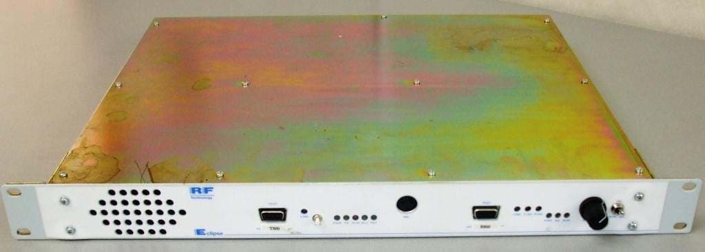
KRE1UTR800CN
Jul 28, 2011UHF BASE STATION
Equipment Class
TNB - Licensed Non-Broadcast Station Transmitter