LNQ802P125Wireless LAN PCI Device
Actiontec Electronics Inc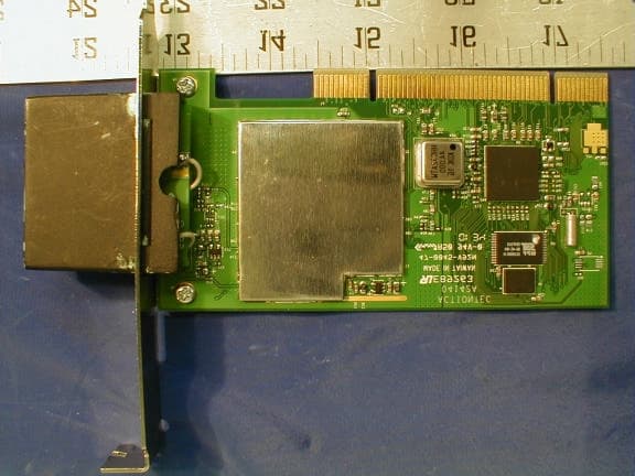
Click to zoom
Application Details
- Equipment Class
- DSS - Part 15 Spread Spectrum Transmitter
- Date of Grant
- Oct 23, 2001
- Application Purpose
- Original Equipment
- Date of Application
- Oct 23, 2001
- Equipment Note
- Wireless LAN PCI Device
- Frequency Range
- 2412.80000000 - 2462.00000000
- Company
- Actiontec Electronics Inc
- Country
- United States
Documents & Files
Document Text
Text extracted from the exhibit documents filed with the FCC. Open a document above to read the original.
Users Manual
SPECIFICATIONS of Low Profile PCI 802.11b Card: 802PI25 Version 0.5 Date: 08/09/01 Specifications of Low Profile PCI 802.11b Card 2 Contents: Device Overall Description 802.11 Wireless LAN - Features - Block Diagram - Modulation Methods - Channel Assignment - Security (WEP Key) - PCI PME & Vaux - RF Characteristics - Software & OS support - Regulation - Interoperability Operating Conditions Device Overall Description The 802PI25 is designed to provide wireless LAN function on a Low Profile PCI form factor. The wireless LAN function is based on Intersil Prism 2.5 chipset, which implements the full IEEE802.11b standard date rates up to 11Mbps. Specifications of Low Profile PCI 802.11b Card 3 802.11 Wireless LAN Features - Intersil Prism II.V chipset - IEEE802.11 Direct Sequence Spread Spetrum (DSSS) - IEEE802.11 Standard Data Rates: 1, 2, 5.5 and 11Mbps - Full Implementation of the MAC Protocol Specified in IEEE Standards 802.11-1999 and 802.11b - Internal Encryption Engine Executes IEEE802.11 WEP - 128-bit WEP encryption, backward compatible with 64-bit solutions. - Support BSS (Infrastruture mode) and IBSS (Ad hoc mode). - Support BSS and IBSS operation under Distributed Coordination Function (DCF) and Ponit Coordination Function (PCF) - Support Psuedo IBSS mode which allows two computers to communicate in Ad Hoc configuration and allows backward compatibility with previous generation of Intersil products. - Onboard Diversity Antenna Specification Compliance - IEEE 802.11b - PCI Bus Interface Spec. 2.2 Form factor - Low Profile PCI Card MD1 form factor - 119.91mm x 64.41mm (LxH) 802.11 Wireless LAN Block Diagram ICW3874A:Intersil, Wireless LAN integrated Medium Access Controller with Baseband Processor ICW3783:Intersil, I/Q Modulator/Demodulator and Synthesizer ICW3183:Intersil, 748MHz Voltage Controlled Oscillator ICW3685:Intersil, 2.4GHz RF/IF Converter and Synthesizer ICW3984:Intersil, 2.4GHz Power Amp and Detector PCI 3874A MAC+BBP SRAM FLASH CLOCK 3783 MODEM SYNT VCO CLOCK 3685 RF/IF CONVERTER VCO DIVERSITY SW. 3984 POWER AMP Specifications of Low Profile PCI 802.11b Card 4 Modulation Methods Modulationspec. 1 MbpsDBPSK802.11 2 MbpsDQPSK802.11 5.5 MbpsCCK802.11b 11 MbpsCCK802.11b Channel Assignment ChannelFrequencyFCCICETSIFranceJapan 12412MHzXXXX 22417MHzXXXX 32422MHzXXXX 42427MHzXXXX 52432MHzXXXX 62437MHzXXXX 72442MHzXXXX 82447MHzXXXX 92452MHzXXXX 102457MHzXXXXX 112462MHzXXXXX 122467MHzXXX 132472MHzXXX 142484MHzX Many countries and region are currently revising the channel assignment. Security (WEP Key) Support the IEEE 802.11b compatible 64 bit WEP in all data rate modes. Support 128 bit 128RC4 algorithm in all data rate modes. PCI PME & Vaux There is no standard specification of Wakeup-on-WirelessLAN defined. Therefore, PME pin is not necessary. The PME pin on PCI bus is not connected to this device. This card is default to get power from PCI +3.3V. There is an option to get power from PCI Vaux pin. Specifications of Low Profile PCI 802.11b Card 5 RF Characteristics RF CharacteristicsMinimumTypicalMaximumUnits Form FactorLow Profile PCI PC Interface32-bit PCIPCI 2.2 Plug and Play CompatibleYes Access Point CapableYes Internal Antenna Impedance50ohms Ambient Operating Temperature Range 070C Storage Temperature Range-20+85C Supply Voltage (3.3 V only)3.03.33.6V RX Supply Current (at 3.3 V)235mA TX Supply Current (at 3.3 V)280mA 802.11 Sleep Supply Current1020mA Initialization Supply Current70mA RX Adjacent Channel Rejection35dB RX Sensitivity, 1 Mbps-90-88dBm RX Sensitivity, 2 Mbps-87-85dBm RX Sensitivity, 5 Mbps-85-83dBm RX Sensitivity, 11 Mbps-83-81dBm Diversity Isolation1520dB TX Output Power+13.5+15dBm TX Carrier Suppression15dB TX Spectral Mask, 1st side-lobe-30dBc TX Spectral Mask, 2nd side-lobe-50dBc 1 Mbps Multipath Tolerance500 nsec802.11 2 Mbps Multipath Tolerance500 nsec802.11 5.5 Mbps Multipath Tolerance200 nsec225 nsec802.11 11 Mbps Multipath Tolerance100 nsec120 nsec802.11 Maximum input Level4dbm Over-voltage protection+17dbm Dual Antenna Diversity, Short PreambleBBP HW Dual Antenna Diversity, Long PreambleBBP HW Preamble LengthShort/Long SRAM128K X 16 Serial Flash128KX8 802.11 ComplianceCompliant Note: Sensitivity based upon 1 kbyte packet length, 8% PER, single antenna driven, diversity enabled. Note: Adjacent channel rejection based upon 1 kbyte packet length, 8% PER, 25 MHz jammer offset. Note: Multipath tolerance based upon 1 kbyte packet length, 8% PER, signal level > -60 dBm, single antenna driven, diversity enabled, broadcast packets. Note: All measurements at the end of 6" of cable through RF Connector with local diversity option. Specifications of Low Profile PCI 802.11b Card 6 Software & OS support OSDriver Win95, OSR2NDIS4 NT4NDIS4 Win98NDIS5 Windows MillenniumNDIS5 Win2000NDIS5 User Configuration UtilityAvailable Regulation USFCC 15.247 CanadaRSS EuropeETSI 300 826 11:1997 ETSI 300 328 11:1996, 2 nd Edition ETSI 300 328 A1 07:1997, 2 nd Edition ERC/DEC/(96) 17, ERC Decision of 1 November 1996 CE Mark JapanTelec Othersupon requested Interoperability Actiontec is an active member of Wireless Ethernet Compatibility Alliance (WECA). All Actiontec 802.11b Wireless product will be certified by WECA Wi-fi test to assure interoperability between vendor’s of 802.11b. Specifications of Low Profile PCI 802.11b Card 7 Operating Conditions Voltage Range3.3V +-0.3V Operating Temperature Range0°C - 65°C Storage Temperature Range-20°C - 85°C Relative Humidity during Operating95% Relative Humidity during Storage95%
External Photos
EUT-Top View EUT- Bottom View
ID Label/Location Info
FCC ID Label Specifications: Text is black or white in color and is left justified. Labels are silk-screened and shall be “permanently affixed” at a conspicuous location on the EUT. Proposed Label Location on EUT FCC ID: LNQ802PI25 Bottom View of EUT FCC ID Label Location
Internal Photos
16.3 EUT- Component View 16.4 EUT – Solder View
Operational Description
Basic Operation Principle of 802PI25 Actiontec Electronics, Inc. 9/2001 Description The Wireless LAN of 802pi25 is a 2.4GHz ISM Band DSSS Radio. It is designed to operate using IEEE 802.11b WLAN Standard for use in wireless networking systems. The Radio consists of 5 major ICs, which are ISL3685, HFA3783, ISL3984, ISL3874A, ISL3183 and few support ICs. It operates at maximum transmit rate 11Mb/s, back off rates 5.5, 2 and 1 Mb/s. The modulation schemes include CCK (Complementary Code Keying), DQPSK and DBPSK depending on what transmit bit rate it operates at. The radio card interfaces to PC through a MiniPCI bus. Main Chips ISL3874A:Intersil, Wireless LAN integrated Medium Access Controller with Baseband Processor HFA3783:Intersil, I/Q Modulator/Demodulator and Synthesizer ISL3183:Intersil, 748MHz Voltage Controlled Oscillator ISL3685:Intersil, 2.4GHz RF/IF Converter and Synthesizer ISL3984:Intersil, 2.4GHz Power Amp and Detector Host Interface The host interface on the 802pi25 is designed specifically for Mini PCI applications. It consists of 32 bits of address and data, as well as all the required Mini PCI control signals. The chip supports the 3.3V signaling environment, with clock speeds up to 33 MHz. Most of the host interface signals are bi-directional. The output slew rates of the signals on 802pi25 have been designed to comply with the Mini PCI Specification, revision 1.0, October 25th 1999. Refer to the standard for a functional description of the Mini PCI signals. Flash A 128K * 8 bits flash chip from SST on the 802pi25. It is used to store the program for the onboard processor. Right after power on, the program will download from flash to SRAM, then the processor execute the program from the SRAM. SRAM A 128K * 16 bits SRAM on the 802pi25. It is used for program downloaded from Flash chip as well as storage buffer for the receiving and transmitting data packet. External LED There is 3 LED status. Once power apply to 802pi25, LED3 will be on. LED1 is used to indicate LINK status; LED2 is used to indicate ACTIVITY status, such as receiving and transmitting. The LED signal go through Mini PCI connector to the host. 44MHz Oscillator The 44MHz oscillator provides almost all the clock for 802pi25. The 44MHz clock is fed into ISL3874 (MAC/BBP), ISL3685 (RF/IF Converter) and HFA3783 (IQ Modem/Synthesizer). For ISL3874, the 44MHz clock is required for the processor to run the program and other circuitry. In ISL3685, the 44MHz clock is used for the internal phase lock loop to keep track the RF frequency from the RF VCO. In HFA3783, the 44MHz clock is used for the internal phase lock loop to keep track the RF frequency from the IF VCO. 44MHz 32KHz Crystal There is a 32KHz crystal connected to ISL3874 chip. The 32KHz clock will only be used in power saving mode. During power saving mode, the 44MHz oscillator will be turned off, and 32KHz will provide clock for the processor in ISL3874. Therefore, minimum of current would be used. RF Connector There are two RF antenna connectors (J1 & J2) onboard to connect to the antenna in the notebook. J1 is to connect to Main antenna; J2 is to connect to Aux. antenna. Main antenna is used for transmitting and receiving while Aux. antenna is for receiving only. Transmitter Path The Ethernet data comes through the MiniPCI interface, the Host I/O interface to the MAC section of ISL3874. The signal then flows into the data router where it is converted from Ethernet to 802.11b protocol. After the signal is converted, a radio preamble and header is added to it and passed to the I/O of BBP (Base Band Processor) section of ISL3874 via PHY I/O, RADIO I/O. There is also support circuitry, such as outboard SRAM and flash ROM, which contains the firmware controlling the radio. In TX modulator of BBP section, differential phase shift keying modulation schemes DBPSK, DQPSK and CCK, with data scrambling capability, are fulfilled to provide a variety of data rates--DBPSK for 1 Mb/s, DQPSK for 2 Mb/s and CCK for 5.5 and 11Mb/s. The signal, which now is two separate quadrature components I and Q, then flows to the quad IF chip HFA3783 through D/A converters. At TX side of BBP, there is also TX ALC (Automatic Level Control) circuitry, which is part of the TX ALC loop. The loop keeps TX output power to be consistent so that prevent the power spectrum from regrowth. HFA3783 is now the dual up conversion mixers (dual down conversion mixers for RX). The signal upconverts to an IF frequency of 374 MHz and passes into a variable gain amplifier, which is also a part of the ALC loop. Next, it passes through the switched TX/RX shared SAW filter into ISL3685 and then upconverts again to a RF frequency from 2.412~2.484 GHz, depending on the channel selection. The signal flows through a pre-amplifier, two band pass filters, which block all the unwanted emissions such as image components, harmonics and spurious stuff, into ISL3984 power amplifier. The output of the power amplifier is then fed through another band pass filter that is about 85 MHz bandwidth to one of the antennas. Receiver Path The receive signal traveling through the air is received by the dual diversity antennas. The circuits will switch to the antenna which provides better RSSI (Received Signal Strength Indication). The RF signal then feeds into an 85 MHz band pass filter, which blocks all the unwanted components such as image frequency. The signal again is amplified using the LNA within ISL3685 and mixed down to the IF frequency of 374 MHz. The PLL and synthesizer select the channel frequency using Low Side Injection. The mixer outputs are then fed through the IF SAW filter that provides image rejection into HFA3783, which is now a quad down converter. HFA3783 also provides RSSI to BBP of ISL3874. There is a two stage analog AGC (Automatic Gain Control) circuit which adjusts the gain to compensate the signal strength differences. The output of the twin AGC’s provides a constant level signal to the I and Q down conv…
Text truncated - open the document above for the full version.
Schematics
Pcgerber II V 5.0 : Thu Sep 27 11:28:15 2001 - (Untitled) : assm_top.art Pcgerber II V 5.0 : Thu Sep 27 11:28:17 2001 - (Untitled) : bottom.art Pcgerber II V 5.0 : Thu Sep 27 11:28:23 2001 - (Untitled) : gnd.art Pcgerber II V 5.0 : Thu Sep 27 11:28:33 2001 - (Untitled) : past_top.art Pcgerber II V 5.0 : Thu Sep 27 11:28:35 2001 - (Untitled) : silk_top.art Pcgerber II V 5.0 : Thu Sep 27 11:28:36 2001 - (Untitled) : solder_bot.art Pcgerber II V 5.0 : Thu Sep 27 11:28:36 2001 - (Untitled) : solder_top.art Pcgerber II V 5.0 : Thu Sep 27 11:28:38 2001 - (Untitled) : top.art Pcgerber II V 5.0 : Thu Sep 27 11:28:51 2001 - (Untitled) : vcc.art
Schematics
Pcgerber II V 5.0 : Thu Sep 27 11:29:59 2001 - (Untitled)
Test Report
Note: This report may not be duplicated without prior written consent of Bay Area Compliance Laboratory Corporation. This report must not be used by the client to claim product endorsement by NVLAP or any agency of the U.S. Government. FCC PART 15 SUBPART C EMI MEASUREMENT AND TEST REPORT For Actiontec Electronics, Inc. 760 North Mary Avenue Sunnyvale, CA 94086 FCC ID: LNQ802PI25 October 10, 2001 This Report Concerns: Original Report Equipment Type: Wireless LAN PCI Device Test Engineer: Jeff Lee Test Date: September 27, 2001 Reviewed By: John Y. Chan – Engineering Manager Prepared By: Bay Area Compliance Laboratory Corporation 230 Commercial Street, Suite 2 Sunnyvale, CA 94085 Tel: (408) 732-9162 Fax: (408) 732 9164 Actiontec Electronics, Inc. FCC ID: LNQ802PI25 Report # R0109271.doc FCC Part 15.247 Test Report Page 2 of 45 TABLE OF CONTENTS 1 - GENERAL INFORMATION.................................................................................................................................4 1.1 PRODUCT DESCRIPTION FOR EQUIPMENT UNDER TEST (EUT)..............................................................................4 1.2 OBJECTIVE............................................................................................................................................................4 1.3 RELATED SUBMITTAL(S)/GRANT(S)......................................................................................................................4 1.4 TEST METHODOLOGY............................................................................................................................................4 1.5 TEST FACILITY......................................................................................................................................................5 1.6 TEST EQUIPMENT LIST AND DETAILS....................................................................................................................6 1.7 EQUIPMENT UNDER TEST (EUT)...........................................................................................................................6 1.8 HOST SYSTEM CONFIGURATION LIST AND DETAILS.............................................................................................6 1.9 LOCAL SUPPORT EQUIPMENT LIST AND DETAILS..................................................................................................7 1.10 EXTERNAL I/O CABLING LIST AND DETAILS.......................................................................................................7 2 - SYSTEM TEST CONFIGURATION....................................................................................................................8 2.1 JUSTIFICATION......................................................................................................................................................8 2.2 EUT EXERCISE SOFTWARE...................................................................................................................................8 2.3 SPECIAL ACCESSORIES..........................................................................................................................................8 2.4 SCHEMATICS / BLOCK DIAGRAM..........................................................................................................................8 2.5 EQUIPMENT MODIFICATIONS................................................................................................................................8 2.6 CONFIGURATION OF TEST SYSTEM........................................................................................................................9 2.7 TEST SETUP BLOCK DIAGRAM............................................................................................................................10 3 - SUMMARY OF TEST RESULTS.......................................................................................................................11 4 - CONDUCTED OUTPUT POWER MEASUREMENT.....................................................................................12 4.1 STANDARD APPLICABLE.....................................................................................................................................12 4.2 MEASUREMENT PROCEDURE...............................................................................................................................12 4.3 MEASUREMENT RESULT......................................................................................................................................12 4.4 TEST EQUIPMENT................................................................................................................................................12 5 – SPURIOUS EMISSION.......................................................................................................................................16 5.1 STANDARD APPLICABLE.....................................................................................................................................16 5.2 MEASUREMENT PROCEDURE...............................................................................................................................16 5.3 MEASUREMENT DATA.........................................................................................................................................16 6 – POWER DENSITY...............................................................................................................................................23 6.1 STANDARD APPLICABLE.....................................................................................................................................23 6.2 MEASUREMENT PROCEDURE...............................................................................................................................23 6.3 TEST RESULTS.....................................................................................................................................................23 7 – 6 DB BANDW…
Text truncated - open the document above for the full version.
Test Setup Photos
Conducted Emission – Front View Conducted Emission – Rear View Radiated Emission – Front View Radiated Emission – Rear View
Contact Information
Applicant
Brian Henrichs(President)
Technical Contact
Bay Area Compliance Laboratory Corp.John Chan
[email protected]408 732 9162
230 Commercial Street · Sunnyvale, Alaska · United States
Test Firm
Bay Area Compliance LaboratoryJohn Chan
Technical Specifications
| # | Rule Parts | Frequency Range | Power Output |
|---|---|---|---|
| 1 | 15C | 2.41 GHz - 2.46 GHz | 35.00 mW |
Other Applications from Actiontec Electronics Inc
LNQWF672
Dec 26, 2025Wi-Fi 7 Outdoor Mesh AP
Equipment Class
DTS - Digital Transmission System
LNQ-WF670G
Dec 09, 2025Wi-Fi 7 Outdoor Mesh AP
Equipment Class
DTS - Digital Transmission SystemLNQ-WF815-2
Apr 14, 2024Tri-band Wi-Fi 6E Wireless AP
Equipment Class
DTS - Digital Transmission System
LNQ-WF825
Mar 24, 2024Tri-band Wi-Fi 7 Wireless AP
Equipment Class
6ID - 15E 6 GHz Low Power Indoor Access Point
LNQ-WF810G-2
Mar 23, 2024Wi-Fi 6E Mesh Extender
Equipment Class
DTS - Digital Transmission System