LNQ802PAG802.11g 802.11a/g WLAN Dual Band PCI Adapter
Actiontec Electronics Inc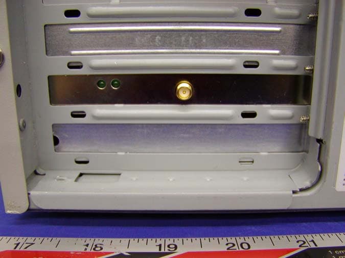
Click to zoom
Application Details
- Equipment Class
- NII - Unlicensed National Information Infrastructure TX
- Date of Grant
- Dec 10, 2003
- Application Purpose
- Original Equipment
- Date of Application
- Dec 10, 2003
- Equipment Note
- 802.11g 802.11a/g WLAN Dual Band PCI Adapter
- Frequency Range
- 5740.00000000 - 5810.00000000
- Company
- Actiontec Electronics Inc
- Country
- United States
Documents & Files
Document Text
Text extracted from the exhibit documents filed with the FCC. Open a document above to read the original.
Users Manual
USER INSTALLATION MANUAL Of Wireless LAN 802.11a/g Dual Band PCI Adapter 802PAG Version: 01 Date: 09/03/03 User Manual of Wireless LAN 802.11a/g Dual Band PCI Adapter 2 Contents: 802.11a/g Wireless LAN - Device Description - System Requirements - Windows 2000 - LED Indicator - Regulatory Compliance Information User Manual of Wireless LAN 802.11a/g Dual Band PCI Adapter 3 Device Description The 802PAG is a Wireless PCI adapter to support IEEE 802.11b/g and/or 802.11a standard. This adapter can be configured to support either 802.11b/g only or 802.11abg standard. System Requirements Desktop PC containing: - 32-bit PCI Bus slot - 32 MB memory or greater - 300 MHz processor or higher Microsoft Windows 2000 / Windows Me / Windows 98 second Edition / Windows XP / Windows NT 4.0 (with Service Pack 6) User Manual of Wireless LAN 802.11a/g Dual Band PCI Adapter 4 Windows 2000 Driver Installation (First-Time Installation) This section describes the 1 st time installation for the driver for Windows 2000. Insert 802PAG into a PCI Bus slot and follow these steps to install the NDIS driver: 1. Wait for the Found New Hardware Wizard dialog box to display. 2. Click Next to continue. 3. Choose “search for a suitable driver for my device (recommended).” 4. Click Next. 5. Insert the release CD into the CD-ROM drive. 6. Choose Specify a location under “Optional search location.” 7. Click Next to continue. 8. Browse to the NDIS driver directory. 9. Click OK to continue. 10. The NDIS evaluation driver currently does not have a digital signature from Microsoft. Therefore, Windows 2000 shows a warning message. Click ‘Yes’ to proceed with driver installation. 11. Click Finish to complete the driver installation. User Manual of Wireless LAN 802.11a/g Dual Band PCI Adapter 5 ACU Installation and Driver Update There is an InstallShield utility to upgrade the NDIS driver, if a previous release is installed, and to install the Atheros Client Utility (ACU). When an NDIS driver has been previously installed, insert the 802PAG into a PCI Bus. Follow these steps to update the NDIS driver: 1. Open the InstallShield Wizard (setup.exe). 2. Click Next to continue. 3. Click ‘Yes’ to accept the License Agreement. 4. The Setup Type page provides selections as summarized in Table 1. Choose the selection appropriate for your network. Table 1. Setup Type Page Selections Selection Description Install Driver and ACU Recommended. Updates driver and installs the ACU. Install Driver Only Installs NDIS driver only Install ACU Only Installs ACU only. Make Driver Installation Diskettes Creates ACU installation diskettes. 5. Click Next to continue. 6. Choose the destination location. Click Next to continue. 7. Specify the program folder to store start icons. 8. Use the checkbox to enable the ACU tray icon and start the ACU when restarting the system. The tray icon will appear in the Windows System Tray. 9. If a previous release of the ACU is installed, make sure it isnot currently running. Click Next to continue If you are running a previous version of the ACU, a dialog box will appear requesting an exit from the program. Click OK and continue. 10. The Atheros NDIS evaluation driver currently does not have a digital signature from Microsoft, so Windows 2000 may show a warning message. Click Yes to proceed with driver installation. 11. Click Finish when the InstallShield Wizard is complete. User Manual of Wireless LAN 802.11a/g Dual Band PCI Adapter 6 Driver and ACU uninstallation This section provides information about uninstallation procedures. To uninstall the ACU and the NDIS driver: Use the InstallShield Updater to uninstall the NDIS driver and ACU application and remove them from the Device Manager. 1. Open the InstallShield Wizard (setup.exe). 2. Click Next to continue. 3. Click ‘Yes’ to accept the License Agreement. 4. On the Setup Type page, choose Uninstall Driver and Applications to uninstall drivers and ACU. Click Next to contine. 5. Click Finish when the InstallShield Wizard is complete. Some files left on the system to ease reinstallation. Use the following instruction to completely remove these files. 1. Go to the Start menu and choose Search For Files or Folder... 2. Enter oem*.inf in the “Search for files or folders named “field”, and enter Atheros in the “Containing text:” field. 3. Click Search Now. A few files matching these criteria are possible, if previous drivers have not been removed properly. 4. Choose the files that have been found and delete them from the system. 5. To complete the uninstallation, remove the file ar5211.sys from the \WINNT\system32\drivers folder. Device Configuration Use the ACU to configure the device driver. The ACU provides extensive online help to aid in configuring the device. Access ACU by clicking the Start button and choosing Programs > Atheros >ACU. The ACU tray icon is displayed in the right side of the Toolbar. Launch the ACU by double- clicking the tray icon, or by right-clicking the tray icon and selecting Launch Station utility. User Manual of Wireless LAN 802.11a/g Dual Band PCI Adapter 7 LED Indicator There are two LED indicators. LED Functionality LED0 (Power) LED1 (Netowrk) Meaning Comments Slow-rate blink OFF Power save mode (default from power up or reset) ON OFF Awake The hardware automatically enter this state after exit from power save mode before any other activity. Changes from power save mode to this state might not be visible on the LEDs if the software assumes control of the LED blinking by writing to the PCI configuration register. Alternate blink Alternate blink Looking for network association Power LED goes ON; Network LED is OFF; then Power LED goes OFF and Network LED goes ON Slow-rate blink Slow-rate blink Associated or joint with network; no activity Fast-rate blink Fast-rate blink Associated or joint with network; blink rate increases with activity on the network over the air or locally on the network device based on setting of the PCI configuration register O…
Text truncated - open the document above for the full version.
Block Diagram
802PAG Block Diagram AR5212: MAC/Baseband Processor for IEEE 802.11a/b/g Wireless LANs AR5112: Radio-on-a-Chip for 5/2.4-GHz Wireless LANs AR2112: Radio-on-a-Chip for 2.4-GHz Wireless LANs /AR21
External Photos
EXHIBIT C - EUT EXTERNAL PHOTOGRAPHS Desktop Front View Desktop Rear View 1 EUT Desktop Rear View 2 EUT Antenna View
ID Label/Location Info
EXHIBIT A - FCC ID LABEL INFORMATION Proposed FCC ID Label Specifications: Text is black or white in color and is left justified. Labels are silk-screened and shall be “permanently affixed” at a conspicuous location on the EUT. Proposed Label Location on Notebook Rear Side of Notebook / Label Location FCC ID: LNQ802PAG This device complies with Part 15 o the FCC Rules. Operation is subject to the following two conditions: (1) this device may not cause harmful interference, and (2) this device must accept any interference received, including interference that may cause undesired operation. 2.1875" 1.0" FCC ID: LNQ802PAG This device complies w ith Part 15 o the FCC Rules. Operation is subject to the following two conditions: (1) this device may not cause harmful interference, and (2) this device must accept any interference received, including interference that m ay cause undesired operation. 2.1875" 1.0"
Internal Photos
EXHIBIT C - EUT INTERNAL PHOTOGRAPHS EUT – Component View EUT – Solder View EUT with Antenna View
Operational Description
802PAG Theory of Operation AR5212: MAC/Baseband Processor for IEEE 802.11a/b/g Wireless LANs AR5112: Radio-on-a-Chip for 5/2.4-GHz Wireless LANs AR2112: Radio-on-a-Chip for 2.4-GHz Wireless LANs The AR5212 is the origin and destination for all the front-end signals. Both transmit (Tx) and receive (Rx) signals are transferred by the AR5112 to either a 5GHz front-end, or a 2.4GHz front end. The 5GHz and the 2.4GHz front ends share a single set of antennae, dual band switch, Rx diplexer, Tx diplexer/low pass filter, coupler, and power detect circuitry. The 5GHz transmit signal is boosted with output booster (OPB). The output booster drives a diplexer and a coupler/detector (PDET) assembly. The diplexer’s function is to combine the 5GHz and 2.4GHz signals. While the coupler/detector's function is to sample the transmit signal and rectify it. The rectified signal is proportional to the output power and is used for power leveling and control. The RF transmit signal then passes through a dual band switch. The switch enables the connection of the input to either one of the two antennae. The 5GHz receive signal is transferred in a reverse order from the antenna through the switch and receive diplexer. It is then boosted using a Low Noise Amplifier (LNA) and fed back into the AR5112. The transmit and receive 2.4GHz signals follow a similar path as the 5GHz signals in the 2GHz front-end. /AR21
RF Exposure Info
RF EXPOSURE According to §15.247(b)(4) and §1.1307(b)(1), systems operating under the provisions of this section shall be operated in a manner that ensures that the public is not exposed to radio frequency energy level in excess of the Commission’s guidelines. According to §1.1310 and §2.1093 RF exposure is calculated. Limits for Maximum Permissive Exposure (MPE) Frequency Range (MHz) Electric Field Strength (V/m) Magnetic Field Strength (A/m) Power Density (mW/cm 2 ) Averaging Time (minute) Limits for General Population/Uncontrolled Exposure 0.3-1.34 614 1.63 *(100) 30 1.34-30 824/f 2.19/f *(180/f 2 ) 30 30-300 27.5 0.073 0.2 30 300-1500 / / f/1500 30 1500-15000 / / 1.0 30 f = frequency in MHz * = Plane-wave equivalent power density MPE Prediction Predication of MPE limit at a given distance Equation from page 18 of OET Bulletin 65, Edition 97-01 S = PG/4πR² Where: S = power density P = power input to antenna G = power gain of the antenna in the direction of interest relative to an isotropic radiator R = distance to the center of radiation of the antenna Maximum peak output power at antenna input terminal: 19.2 (dBm ) Maximum peak output power at antenna input terminal: 83.18 (mW) Prediction distance: 20 (cm) Predication frequency: 5200 (MHz) MPE limit for uncontrolled exposure at prediction frequency: 1 (mW/cm^2) Maximum Antenna Gain (typical): 1.1 (dBi) Maximum antenna gain: 1.29 (numeric) Power density at predication frequency at 20 cm: 0.018 (mW/cm 2 ) Test Result The predicted power density level at 20 cm is 0.018 mW/cm^2. This is below the uncontrolled exposure limit of 1mW/cm^2 at 5200 MHz. The EUT is used at least 3cm away from user’s body, so it is determined as mobile equipment.
Schematics
ACTIONTEC 802PAG802.11abg PCI CARD REVISION HISTORY:5/29/03 REV. 1A 0521 Cover Page 2A 802PAG C 17 Thursday, August 28, 2003 Actiontec Electronics, Inc. TitleSize Document Number Rev Date: Sheet of U7BRACKET 12 UP BOT CC10_NL 1 2 CC20_NL 1 2 AR5212 MAC/BBP 2A 802PAG C 27 Thursday, August 28, 2003 Actiontec Electronics, Inc. TitleSize Document Number Rev Date: Sheet of PCI_PERR_L PCI_PERR_L AD12 AD12 AD13 AD13 AD28 AD28 AD6 AD6 AD29 AD29 AD3 AD3 AD5 AD5 PCI_INT_L PCI_INT_L AD21 AD21 PCI_STOP_L PCI_STOP_L AD16 AD16 PCI_PAR PCI_PAR IDSEL PCI_CBE0_L PCI_CBE0_L EPRM_DIEPRM_CLK DACP_I DACN_I EPRM_CS ADCN_I AD31 AD31 AD8 AD8 PCI_CBE1_L PCI_CBE1_L AD4 AD4 AD15 AD15 AD30 AD30 AD10 AD10 RFDATAIN ATTEN5GPIO_3 ADCRES PCI_SERR_L PCI_SERR_L AD11 AD11 RFDATAOUT3 AD2 AD2 PCI_TRDY_L PCI_TRDY_L AD19 AD19 ADCP_IADCP_Q TX5 EPRM_EN_LRX_CLEARHITUNE5 AD1 AD1 AD23 AD23 PCI_2_CLK SLEEP EPRM_DO ADCISEL AD7 AD7 XIN RFLOADRFRESET_L PCI_FRAME_L PCI_FRAME_L RFDATAOUT1RFDATAOUT0 DACN_Q ADCN_Q RFSHIFTRFDATAOUT2AR5112_CLK40_OUT LEDO_0LEDO_1 GPIO_0 DACP_Q PCI_RST_L PCI_RST_L PCI_CLKRUN_L PCI_CLKRUN_L AD0 AD0 AD9 AD9 AD14 AD14 AD17 AD17 AD18 AD18 AD20 AD20 AD22 AD22 AD24 AD24 AD25 AD25 AD26 AD26 AD27 AD27 PCI_CBE2_L PCI_CBE2_L PCI_CBE3_L PCI_CBE3_L PCI_REQ_L PCI_REQ_L PCI_GNT_L PCI_GNT_L PCI_IRDY_L PCI_IRDY_L PCI_DEVSEL_L PCI_DEVSEL_L PCI_PME_L PME_L XOUT RX5 F2D2EN LED0 LED1 ATTEN2 TX2 PCI_RST_LPCI_2_CLK PCI_CBE0_LPCI_CBE1_LPCI_CBE2_LPCI_CBE3_LPCI_INT_LPCI_REQ_LPCI_GNT_LPCI_PERR_LPCI_PARPCI_IRDY_LPCI_TRDY_LPCI_FRAME_LPCI_STOP_LPCI_SERR_LPCI_DEVSEL_LIDSELPCI_PME_L AD[0:31] PCI_MODE ADCP_Q 3ADCN_I 3ADCP_I 3 RFDATAIN 3RFRESET_L 3AR5112_CLK40_OUT 3 DACN_Q 3DACP_Q 3DACN_I 3 RX5 4RFSHIFT 3RFDATAOUT0 3RFDATAOUT1 3RFDATAOUT2 3RFDATAOUT3 3RFLOAD 3ANTA 4TX5 4TX2 4 SLEEP 5 DACP_I 3 ADCN_Q 3 ANTB 4 ATTEN2 5 REQ_L 3 CBE2_L 3 IRDY_L 3 CBE1_L 3 SERR_L 3 TRDY_L 3 GNT_L 3 PAR 3 CBE3_L 3 AD[0:31] 3 FRAME_L 3 IDSEL_L 3 DEVSEL_L 3 CBE0_L 3 PCI_CLK 3 PERR_L 3 STOP_L 3 RST_L 3 PCI_PME_L 3 INTA_L 3 GPIO2 5 3.3V 3.3V 3.3V VCC_ADC 3.3V VCC_CORE 3.3V VCC_DAC 3.3V VCC_CORE 3.3V 3.3V 3.3V 3.3V 3.3V R101R 1 2 C353C 12 R113 47 1 2 R104R 1 2 0.01uF 25V C4 TP5 1 0.01uF 25V C6 0.01uF 25V C5 0.01uF 25V C13 0.01uF 25V C12 R9330 12 0.01uF 25V C14 R10330 12 R56 R 1 2 R54R 12 R55R 12 R103R 12 R108R 12 R109R 12 22pF C2 R1020 12 AR5212 U1 N7 K13 L14 M14 N13N12 M11 N11 P10 P4 N3 C2A3 N6 K14 N8 K12 L12 N14 P13P12 D9 P11 N5 M4 A2 J1 C1H12 B3 P2 L13 M13 M7 G3 D1 M9 P5 N4 L1 G14J13 A4 B4 C4 P7 E4 D11 G4 H4 E5 K4 E6 J14 D6 F14 A5 B5 G12 D5 N2 B13 E7 E8 E9 E10 L5 M5 F12A14 A6 B6 C7 F4 F5 F6 F7 F8 F9 F10 F11 C12 E1A1 A7 B7 C6 D7 G5 G6 G7 G8 G9 G10 L7 H3 B1E13 A8 B8 C8 D8 H5 H6 H7 H8 H9 H10 L8 P3 E12F3 A9 B9 C9 J4 J5 J6 J7 J8 J9 J10 J11 D4 H14H13 A10 B10 C10 D10 K5 K6 K7 K8 K9 K10 L10 M10 D3D2 A11 B11C11 L4 E11 L6 G11 H11 L9 K11 L11 E2E3G13A12B12 M3 D12C14 C3 P8P9 B2 L2 K1 M12 J12 C5 A13F2C13D13 N10 M6 N1N9 M2 K3 J3 P1 F1H2H1B14E14D14F13 M1M8 P6 L3 K2 J2 P14 G2G1 PCI_TRDY_L PCI_AD1PCI_AD3PCI_AD6PCI_AD9PCI_AD11PCI_AD13PCI_AD14PCI_AD16PCI_AD19PCI_AD22 TDO TMS PCI_FRAME_LPCI_AD0PCI_STOP_LPCI_AD2PCI_AD5PCI_AD8PCI_AD10PCI_AD12 GND PCI_AD15PCI_AD18PCI_AD21 TDI PCI_CLKRUN_L TCLK SLEEP AGND PCI_SERR_LPCI_AD4PCI_AD7PCI_DEVSEL_L VDD2_5 RX2 PCI_IDSELPCI_AD17PCI_AD20PCI_PME_L GPIO_5 ANTB ADC_QN ADC_QP AVDD_ADC PCI_CLK VDD3_3 GND VDD2_5 VDD2_5 GND VDD3_3 GND ANTA GND F2D2EN AGND AGND HITUNE5 VDD3_3 GND GND GND GND GND GND VDD3_3 VDD3_3 ANTD RFDATAOUT_0 ADC_IP ADC_IN ADCISEL GND GND GND GND GND GND GND GND GND RX5 EPRM_EN_L AGND AVDD_ADC ADCRES VDD2_5 GND GND GND GND GND GND VDD2_5 VDD2_5 TRST_L TX2 DAC_QN DAC_QP AVDD_DAC VDD2_5 GND GND GND GND GND GND VDD2_5 PCI_RST_L TX5 RX_CLEAR AGND AGND AVDD_DAC GND GND GND GND GND GND GND GND GND LED_1LED_0 DAC_IP DAC_IN AVDD_PLL VDD3_3 GND GND GND GND GND GND VDD3_3 VDD3_3 GPIO_1GPIO_0 AGND XIN XOUT GND VDD3_3 GND VDD2_5 VDD2_5 GND VDD3_3 GND GPIO_2GPIO_3GPIO_4 RFRESET_L RFLOAD GND ANTC RFDATAOUT_3 GND PCI_INT_LPCI_PERR_L GND PCI_AD26PCI_AD29 GND ATTEN2 PCI_MODE RFSHIFT EPRM_DO RFDATAOUT_2 RFDATAIN5 PCI_CBE1_L PCI_CBE2_LPCI_REQ_LPCI_PARPCI_AD24PCI_AD27PCI_AD30PCI_AD23 EPRM_DI ATTEN5 EPRM_CLK RFDATAOUT_1 PLLBYPASS REFCLK CLKOBS PCI_CBE3_L PCI_GNT_LPCI_IRDY_LPCI_AD25PCI_AD28PCI_AD31PCI_CBE0_L RFDATAIN2 EPRM_CS TP8 1 0.1uF 10V C8 0.1uF 10V C7 0.1uF 10V C15 0.1uF 10V C9 R11210K 12 0.1uF 10V C17 0.1uF 10V C16 3.9M R1 32.768KHZ Y3 1 4 R510K_NL 12 AT93C86-10TI-2.7 U2 1234 5678 CSSKDIDO GND NCNC VCC R R8 6.19K 1% R2 DS1 LTST-C 190GKT R610K_NL 12 22pF C1 R710K_NL 12 TP4 1 DS2 LTST-C 190GKT 10pF C10 32.768KHZ Y1 1 4 10pF C18 10pF C11 10pF C19 TP6 1 TP2 1 TP3 1 R11110K 12 TP7 1 22pF C3 TP1 1 55 44 33 22 11 D D C C B B A A Place C39 close to pin 45 Place C45 close to pin 43 AR5112 RF CHIP 2A 802PAG C 37 Thursday, August 28, 2003 Actiontec Electronics, Inc. TitleSize Document Number Rev Date: Sheet of ADCP_IDACN_IADCP_Q RFRESET_LRFLOADRFSHIFTRFDATAOUT0RFDATAOUT1RFDATAOUT2RFDATAOUT3RFDATAIN PDETECT5 PDETECT AR5112_CLK40_OUT AR5112_5G_RX_IN ADCN_QADCN_IDACP_I XBIAS5 DACP_QDACN_Q XBIAS2 PDETECT2 RFRESET_L 2 RFSHIFT 2 RFDATAOUT0 2 RFDATAOUT1 2 RFDATAOUT2 2 RFDATAOUT3 2 ADCN_Q 2 ADCP_Q 2 ADCP_I 2 ADCN_I 2 DACP_Q 2 DACN_Q 2 DACP_I 2 DACN_I 2 AR5112_2G_RX_IN 4 AR5112_5G_RX_IN 4 RFDATAIN 2 RFLOAD 2 PDETECT 4 AR5112_CLK40_OUT 2 XBIAS2 4 XBIAS5 4 AR5112_2G_TX_OUT_N 4 AR5112_2G_TX_OUT_P 4 AR5112_5G_TX_OUT_P 4 AR5112_5G_TX_OUT_N 4 2.5V_A 2.5V_A 2.5V_A 2.5V_A 2.5V_A 3.3V_A 2.5V_A 3.3V_A 3.3V_VCO 2.5V_D 2.5V_A 2.5V_A 3.3V_A 2.5V_A 2.5V_A 0.1uF 10V C52 0.1uF 10V C51 0.1uF 10V C77 1pF C68 12 6.19K 1% R25 AR5112 DUAL BAND U3 123456789 12111315141016 28 27 26 25 24 23 22 29 30 31 32 33343736 21 35 19 17 18 38 20 39434445474846 49 50 52 53 54 55 56 57 58 59 51 60 62 63 64 424041 61 65 Gnd2aRESET_LSerial_loadSerial_clkSerial_in0Serial_in1Serial_in2Serial_in3Vdd2dClk40DataOutGnd3dVdd2aVdd3dGnd2dXtal_i Aoutp_dc RF5out_p RF5out_n Aoutn_dc Ares Vdd3pa Gnd2a Gnd2a Vdd3pa Gnd2a Vdd2a Pdetect5Pdetect2 Boutp_dc Bres Vdd2a Vdd2pa xbias5 Xtal_o xbias2 RF2out_p Biasref RF2out_p Vdd2pa …
Text truncated - open the document above for the full version.
Test Report
Note: This test report is specially limited to the above client company and product model only. It may not be duplicated without prior written consent of Bay Area Compliance Laboratory Corporation. This report must not be used by the client to claim product endorsement by NVLAP or any agency of the U.S. Government. FCC PART 15 EMI Measurement and TEST REPORT For Actiontec Electronics, Inc. 760 North Mary Ave. Sunnyvale, CA 94086 FCC ID: LNQ802PAG 2003-10-08 This Report Concerns: Original Report Equipment Type: 802.11a/g WLAN Dual Band PCI Adapter Test Engineer: Ling Zhang / Report No.: R0309022 Test Date: 2003-09-05 / 2003-09-08 / 2003-09-09 / 2003-09-16 / 2003-09-17 / 2003-09-18 Reviewed By: Ming Jing / Prepared By: Bay Area Compliance Laboratory Corporation (BACL) 230 Commercial Street Sunnyvale, CA 94085 Tel: (408) 732-9162 Fax: (408) 732 9164 Actiontec Electronics, Inc. FCC ID: LNQ802PAG Report # R0309022Rpt.doc Page 2 of 108 FCC Part 15.247 & 15.407 Test Report TABLE OF CONTENTS 1 - GENERAL INFORMATION..................................................................................................................................4 1.1 PRODUCT DESCRIPTION FOR EQUIPMENT UNDER TEST (EUT) ..............................................................................4 1.2 OBJECTIVE.............................................................................................................................................................4 1.3 RELATED SUBMITTAL(S)/GRANT(S).......................................................................................................................4 1.4 TEST METHODOLOGY............................................................................................................................................4 1.5 TEST FACILITY.......................................................................................................................................................5 1.6 TEST EQUIPMENT LIST...........................................................................................................................................5 1.7 SUPPORT EQUIPMENT LIST AND DETAILS..............................................................................................................6 1.8 EXTERNAL I/O CABLING LIST AND DETAILS.........................................................................................................6 2 - SYSTEM TEST CONFIGURATION.....................................................................................................................7 2.1 JUSTIFICATION.......................................................................................................................................................7 2.2 EUT EXERCISE SOFTWARE....................................................................................................................................7 2.3 SPECIAL ACCESSORIES...........................................................................................................................................7 2.4 SCHEMATICS / BLOCK DIAGRAM...........................................................................................................................7 2.5 EQUIPMENT MODIFICATIONS.................................................................................................................................7 2.6 CONFIGURATION OF TEST SYSTEM.........................................................................................................................8 2.7 TEST SETUP BLOCK DIAGRAM...............................................................................................................................8 3 - SUMMARY OF TEST RESULTS..........................................................................................................................9 4 - PEAK OUTPUT POWER MEASUREMENT ....................................................................................................10 4.1 STANDARD APPLICABLE......................................................................................................................................10 4.2 MEASUREMENT PROCEDURE................................................................................................................................10 4.3 EQUIPMENT LISTS................................................................................................................................................11 4.4 MEASUREMENT RESULT......................................................................................................................................11 5 – 6 DB BANDWIDTH AND 26 DB BANDWIDTH...............................................................................................20 5.1 STANDARD APPLICABLE......................................................................................................................................20 5.2 MEASUREMENT PROCEDURE................................................................................................................................20 5.3 EQUIPMENT LISTS................................................................................................................................................20 5.4 MEASUREMENT RESULT......................................................................................................................................20 6 - POWER SPECTRAL DENSITY ..........................................................................................................................30 6.1 STANDARD APPLICABLE......................................................................................................................................30 6.2 MEASUREMENT PROCEDURE................................................................................................................................30 6.3 EQUIPMENT LISTS....................................................................................................................................…
Text truncated - open the document above for the full version.
Test Report
Actiontec Electronics, Inc. FCC ID: LNQ802PAG Report # R0309022Rpt.doc Page 40 of 108 FCC Part 15.247 & 15.407 Test Report 7 - 100 KHZ BANDWIDTH OF BAND EDGES 7.1 Standard Applicable According to §15.247(c), in any 100 kHz bandwidth outside the frequency bands in which the spread spectrum intentional radiator is operating, the radio frequency power that is produced by the intentional radiator shall be at least 20 dB below that in the 100 kHz bandwidth within the band that contains the highest level of the desired power, based on either an RF conducted or a radiated measurement. In addition, radiated emissions which fall in the restricted bands, as defined in §15.205(a), must also comply with the radiated emission limits specified in §15.209(a) see §15.205(c)). 7.2 Measurement Procedure 1. Check the calibration of the measuring instrument using either an internal calibrator or a known signal from an external generator. 2. Position the EUT without connection to measurement instrument. Turn on the EUT and connect its antenna terminal to measurement instrument via a low loss cable. Then set it to any one measured frequency within its operating range, and make sure the instrument is operated in its linear range. 3. Set both RBW and VBW of spectrum analyzer to 100 kHz with a convenient frequency span including 100kHz bandwidth from band edge. 4. Measure the highest amplitude appearing on spectral display and set it as a reference level. Plot the graph with marking the highest point and edge frequency. 5. Repeat above procedures until all measured frequencies were complete. 7.3 Equipment Lists Manufacturer Model No. Description Calibration Due Date Agilent 8564E Spectrum Analyzer 2004-08-26 7.4 Measure Results Please refer to following pages for plots of band edge. Actiontec Electronics, Inc. FCC ID: LNQ802PAG Report # R0309022Rpt.doc Page 41 of 108 FCC Part 15.247 & 15.407 Test Report Plots of Band Edge for 802.11b (15.247) Actiontec Electronics, Inc. FCC ID: LNQ802PAG Report # R0309022Rpt.doc Page 42 of 108 FCC Part 15.247 & 15.407 Test Report Plots of Band Edge for 802.11g (15.247) Actiontec Electronics, Inc. FCC ID: LNQ802PAG Report # R0309022Rpt.doc Page 43 of 108 FCC Part 15.247 & 15.407 Test Report Actiontec Electronics, Inc. FCC ID: LNQ802PAG Report # R0309022Rpt.doc Page 44 of 108 FCC Part 15.247 & 15.407 Test Report 8 - Peak Excursion To Average Ratio 8.1 Standard Applicable According to §15.407(a)(6), the ratio of the peak excursion of the modulation envelope (measured using a peak hold function) to the peak transmit power (measured as specified above) shall not exceed 13dB across any 1MHz bandwidth or the emission bandwidth whichever is less. 8.2 Test Procedure For this test, the EUT’s antenna was removed and replaced with a SAM jack to UMP2.0 plug test calbe, so output power levels were calculated from conducted emission levels. For trace A, set RBW=1MHz, VBW> 3MHz with peak detector and max-hold. For trace B, set average mode. 8.3 Equipment Lists Manufacturer Model No. Description Calibration Due Date Agilent 8564E Spectrum Analyzer 2004-08-26 8.4 Test Result for 15.407 Band Channel Frequency (MHz) Reading (dB) Limit (dBm) Result Low 5165 8.00 13 Compliant Mid 5200 7.17 13 Compliant Low High 5250 8.17 13 Compliant Low 5265 6.84 13 Compliant Mid 5300 7.66 13 Compliant Mid High 5330 7.50 13 Compliant Low 5740 7.33 13 Compliant Mid 5770 7.00 13 Compliant High High 5810 7.33 13 Compliant Please see the hereinafter plots for more detail. Actiontec Electronics, Inc. FCC ID: LNQ802PAG Report # R0309022Rpt.doc Page 45 of 108 FCC Part 15.247 & 15.407 Test Report Actiontec Electronics, Inc. FCC ID: LNQ802PAG Report # R0309022Rpt.doc Page 46 of 108 FCC Part 15.247 & 15.407 Test Report Actiontec Electronics, Inc. FCC ID: LNQ802PAG Report # R0309022Rpt.doc Page 47 of 108 FCC Part 15.247 & 15.407 Test Report Actiontec Electronics, Inc. FCC ID: LNQ802PAG Report # R0309022Rpt.doc Page 48 of 108 FCC Part 15.247 & 15.407 Test Report Actiontec Electronics, Inc. FCC ID: LNQ802PAG Report # R0309022Rpt.doc Page 49 of 108 FCC Part 15.247 & 15.407 Test Report Actiontec Electronics, Inc. FCC ID: LNQ802PAG Report # R0309022Rpt.doc Page 50 of 108 FCC Part 15.247 & 15.407 Test Report 9 - Out Of Band Emission for 15.407 9.1 Standard Applicable §15.407 (b), undesirable emission limits: except as shown in paragraph (b)(6) of this section, the peak emission outside of the frequency bands of operation shall be attenuated in accordance with the following limits: §15.407 (b)(1), for transmitters operating in the 5.15-5.25 GHz band: all emissions outside of the 5.15-5.35 GHz band shall not exceed an EIRP of -27 dBm/MHz. §15.407 (b)(2), for transmitters operating in the 5.25 – 5.35 GHz band: all emissions outside of the 5.15 – 5.25 GHz band shall not exceed an EIRP of –27 dBm/MHz. Devices operating in the 5.25 – 5.35 GHz band that generate emissions in the 5.15 – 5.25 GHz band must meet all applicable technical requirements for operation in the 5.15 – 5.25 GHz band (including indoor use) or alternatively meet an out-of-band emission EIRP limit of –27 dBm/MHz in the 5.15 – 5.25 GHz band. §15.407 (b)(3), for transmitters operating in the 5.725 – 5.825 GHz band: all emissions within the frequency range from the band edge to 10 MHz above or below the band edge shall not exceed an EIRP of –17dBm/MHz; for frequencies 10 MHz or greater above or below the band edge, emission shall not exceed an EIRP of –27 dBm/MHz. 9.2 Test Procedure For this test, the EUT’s antenna was removed and replaced with a low loss cable, so output power levels were calculated from conducted emission levels. The analyzer center frequency was set to the EUT carrier frequency. The analyzer resolution and video bandwidth were set to 1MHz. The entire band from 30kHz to 40GHz was investigated. Every suspected signal was also investigated through radiated emission. Refer to section 15.205 restricted bands of operation. 9.3 Equipment Lists Manufacturer Mode…
Text truncated - open the document above for the full version.
Test Report
Actiontec Electronics, Inc. FCC ID: LNQ802PAG Report # R0309022Rpt.doc Page 70 of 108 FCC Part 15.247 & 15.407 Test Report Plots of Spurious Emission for 802.11a (15.247) Actiontec Electronics, Inc. FCC ID: LNQ802PAG Report # R0309022Rpt.doc Page 71 of 108 FCC Part 15.247 & 15.407 Test Report Actiontec Electronics, Inc. FCC ID: LNQ802PAG Report # R0309022Rpt.doc Page 72 of 108 FCC Part 15.247 & 15.407 Test Report Actiontec Electronics, Inc. FCC ID: LNQ802PAG Report # R0309022Rpt.doc Page 73 of 108 FCC Part 15.247 & 15.407 Test Report Actiontec Electronics, Inc. FCC ID: LNQ802PAG Report # R0309022Rpt.doc Page 74 of 108 FCC Part 15.247 & 15.407 Test Report Actiontec Electronics, Inc. FCC ID: LNQ802PAG Report # R0309022Rpt.doc Page 75 of 108 FCC Part 15.247 & 15.407 Test Report Actiontec Electronics, Inc. FCC ID: LNQ802PAG Report # R0309022Rpt.doc Page 76 of 108 FCC Part 15.247 & 15.407 Test Report Actiontec Electronics, Inc. FCC ID: LNQ802PAG Report # R0309022Rpt.doc Page 77 of 108 FCC Part 15.247 & 15.407 Test Report Actiontec Electronics, Inc. FCC ID: LNQ802PAG Report # R0309022Rpt.doc Page 78 of 108 FCC Part 15.247 & 15.407 Test Report Actiontec Electronics, Inc. FCC ID: LNQ802PAG Report # R0309022Rpt.doc Page 79 of 108 FCC Part 15.247 & 15.407 Test Report
Test Report
Actiontec Electronics, Inc. FCC ID: LNQ802PAG Report # R0309022Rpt.doc Page 80 of 108 FCC Part 15.247 & 15.407 Test Report Actiontec Electronics, Inc. FCC ID: LNQ802PAG Report # R0309022Rpt.doc Page 81 of 108 FCC Part 15.247 & 15.407 Test Report Actiontec Electronics, Inc. FCC…
Text truncated - open the document above for the full version.
Contact Information
Applicant
Brian Henrichs(President)
Test Firm
Bay Area Compliance LaboratoryJohn Chan
Technical Specifications
| # | Rule Parts | Frequency Range | Power Output |
|---|---|---|---|
| 3 | 15E | 5.74 GHz - 5.81 GHz | 94.84 mW |
Other Applications from Actiontec Electronics Inc
LNQWF672
Dec 26, 2025Wi-Fi 7 Outdoor Mesh AP
Equipment Class
DTS - Digital Transmission System
LNQ-WF670G
Dec 09, 2025Wi-Fi 7 Outdoor Mesh AP
Equipment Class
DTS - Digital Transmission SystemLNQ-WF815-2
Apr 14, 2024Tri-band Wi-Fi 6E Wireless AP
Equipment Class
DTS - Digital Transmission System
LNQ-WF825
Mar 24, 2024Tri-band Wi-Fi 7 Wireless AP
Equipment Class
6ID - 15E 6 GHz Low Power Indoor Access Point
LNQ-WF810G-2
Mar 23, 2024Wi-Fi 6E Mesh Extender
Equipment Class
DTS - Digital Transmission System