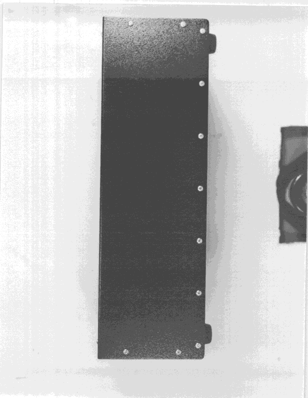
Click to zoom
Application Details
- Equipment Class
- DSS - Part 15 Spread Spectrum Transmitter
- Date of Grant
- Jul 26, 1999
- Application Purpose
- Original Equipment
- Date of Application
- Feb 16, 1999
- Frequency Range
- 2401.00000000 - 2475.00000000
- Country
- United States
Documents & Files
Document Text
Text extracted from the exhibit documents filed with the FCC. Open a document above to read the original.
Operational Description
MKRS416 RECEIVER COMPLIANCE TO PART 15.247(a)(1) General Description The MKRS416 receiver is a homodyne configuration, which uses a local oscillator signal, at the same frequency as the transmitted signal, to downconvert the received signal to baseband. The baseband signal is filtered with a 5-pole Bessel low pass filter, which has a cutoff frequency of 400 KHz. Using a local oscillator signal derived from the transmitter for direct downconversion to baseband insures synchronization of the receiver and transmitter. Using a low pass filter insures the receiver bandwidth matches the hopping channel bandwidth. The combination of these 2 design features provides compliance with Part 15.247(a)(1) in the MKRS416 receiver design. Detailed Description The receiver signal enters through the antenna and is routed through the SP6T switch. The signal then passes through the microwave circulator to a power divider. The two signals from the power divider are quadrature downconverted (to baseband) in 2 mixers, each using a local oscillator signal derived from the transmitter. The 2 baseband signals are amplified and then filtered with a 5-pole Bessel low pass filter. After 2 additional amplification stages, the absolute value of the quadrature channel signals is taken, then these signals are summed together. This final summed signal is compared to a pre-set voltage level to create a logic level signal for the microprocessor.
Operational Description
LP0990021 of 4 Procedure for Taking Submittal Photographs Prepared by Dennis Ward FOR CKC LABORATORIES, INC. 5473A CLOUDS REST ROAD MARIPOSA, CA 95338 U.S.A. Reviewed by: Tracy Phillips © October 2, 1998 Revised July 2, 1999 LP0990022 of 4 TABLE OF CONTENTS 1.0 Purpose........................................................ 3 2.0 Procedure for issuing Work Order for Photographic work......... 3 3.0 Submittal photographs.......................................... 3 LP0990023 of 4 1.0Purpose The purpose of this procedure is to establish a method by which Submittal photographs are to be taken. 2.0Procedure for issuing Work Order for Photographic work 2.1 All testing is verified complete by the CKC test engineer. 2.1. Once tests are verified complete, the Test Engineer contacts the Customer Service Representative / Service Advisor in Mariposa to inform the CSR/SA the device is ready for submittal photographs to be taken and provides the following information to the CSR/SA: 1. The Model number(s) of the device or devices. 2. The serial number(s) of the device or devices. 3. The work order number of the test sequence. 4. The tracking number of the shipment if necessary. 2.2. If photographs are to be taken in Mariposa, the CSR/SA notifies shipping that the device is in route. The CSR/SA provides the tracking number to shipping. When the shipment arrives, shipping notifies the CSR/SA. 2.3. The CSR/SA issues a work order, and schedules the photographs to be taken at the appropriate lab. The CSR/SA insures that the person to whom the work order has been assigned is notified. 3.0Submittal photographs 3.1 Photographs are to be of such quality as to allow the silk-screening on PCB's to be easily read. 3.2 Set the device on the light stand or other appropriately lit area suitable for the photographic quality needed. Use appropriate film ASA number for lighting and meter settings for exposure. Devices too large for the light stand will have to be set up on an alternate location where appropriate lighting is available. The background color should accent the EUT. 3.3 Start the photo log template and record the Customer information along with the model number, serial number and work order number for the device. After each picture is taken as listed below, record pictures in the photo log in the order taken. 3.4 The following is a minimum of pictures to be taken: 1. Top of the device. 2. Bottom of the device. 3. Sides as appropriate. 4. Cables, if hardwired to device. Otherwise remove cable and take a picture of the port connector or connectors. 5. If there is a label on the device, a picture of the label and label placement. 6. Photographs of successive stages of disassembly should be sufficient to give understanding as to how to assemble the device. 7. Photographs taken in the various stages of disassembly need to show the relationship of the various parts and subassemblies to each other. LP0990024 of 4 8. Open the device without moving internal parts or pieces, and take a picture of the top of the device opened and laid out. 9. Turn the device over and take a picture of the bottom side of the open device. 10. Disassemble the device and take pictures of both sides of all boards. 11. Take pictures of the various and successive stages of disassembly. 12. All internal components, including metal, plastic, transparent, or other components. Pictures should show the relationship of all components as close as possible. 13. If the device has shielded or encased enclosures internally, these must be taken apart and pictures of all components taken. If the shielded enclosure internal to the device has PC boards, pictures of both sides of all boards must be taken, as well as any and all other components in the enclosed area. An example of this type enclosure would be a shielded rf section inside an intentional radiator main case. 14. The inside of the top and bottom halves of the outer enclosure, and the inside of the top and bottom of any interior enclosure. 15. All mechanical components in as close proximity of their actual location as possible. 3.5 The person taking the photographs is to process the work order back indicating the submittal photographs have been taken.. 3.6 The film, photo log and device are given to the Report Department for processing. If the work is done for a submittal, the report department keeps the device until approval of the product has been granted. 3.7 The Report Department will have the film immediately developed by the current CKC outsource for this project and in accordance with the work order. 3.8 At the same time, the Report Department will store the device in a secure location. 3.9 Once the film has been developed and returned to CKC, the photographs and negatives will be placed in the file for the device. If a submittal has been ordered, the report department processes the photographs into the submittal package. 3.10 Only after the device has been granted approval by the agency or agencies, will the device be shipped back to the customer as follows: 1. The Report Department will give the device with all information, including the work order, to shipping. 2. Shipping will ship the device back to the customer. 3. Shipping will notify the CSR/SA for that customer that the device has been shipped.
Operational Description
LP0990031 of 4 Procedure for Handling Sample Requests for FCC Testing Prepared by Dennis Ward FOR CKC LABORATORIES, INC. 5473A CLOUDS REST ROAD MARIPOSA, CA 95338 U.S.A. Reviewed by: Tracy Phillips © July 2, 1999 LP0990032 of 4 TABLE OF CONTENTS 1.0Purpose .................................................................................................................. 3 2.0Procedure for issuing Work Order for Sample Request........................................ 3 3.0Sample testing ....................................................................................................... 3 4.0Shipment to the FCC ............................................................................................. 3 LP0990033 of 4 1.0Purpose The purpose of this procedure is to establish a method by which sample requests by the FCC are to be handled. 2.0Procedure for issuing Work Order for Sample Request 2.1 Upon CKC receiving a request for sample from the FCC, a work order will be issued by the Service Advisor (SA/CSR). The purpose of this work order is to perform verification testing on the product before it is sent to the FCC, and to start tracking the sample. 2.2 The work order is distributed to the appropriate test engineer. Note: In the event of larger equipment or equipment that was shipped back to the customer, the SA contacts the customer of the Sample Request from the FCC and requests that the sample be sent to CKC for verification of compliance. CKC's preferred procedure is to hold the EUT until the approval process is complete. However, should the customer insist on having CKC send the product back to them before the process is complete, CKC informs them of the possibility of sample request, and urges clients to send the product to CKC for inspection before shipping to the FCC. It is out of CKC's control if the client chooses to send the product directly to the FCC. In this instance, all aspects of the sample are controlled by the manufacturer. CKC takes no responsibility for samples sent to the FCC that have not gone through the sample request process at CKC. 3.0 Sample testing 3.1 The test engineer assigned the task of verifying the sample prior to shipping to the FCC retrieves the sample from the control of the Report Department. If the product has been shipped to CKC from the client shipping/receiving notifies the SA that the product has arrived. At this time the Test Engineer is also informed and retrieves the sample from shipping/receiving. 3.2 The sample is visually inspected. This is to verify that the product is as shown in the photographs. 3.3 The sample is setup and tested in accordance with the standards used for the submittal. Verification is necessary to make sure that during the process of taking photographs and re-assembly, or shipment from the client, the product remains compliant. 3.4 After the product has been successfully verified compliant, the sample is prepared for shipment. 4.0 Shipment to the FCC 4.1 The test engineer and/or the Report Department completes the forms provided by the FCC. 4.2 Each item in the shipment is tagged with the FCC ID number of the device, name of applicant as written on the 731 form, CKC labs address, phone number, and contact person. LP0990034 of 4 4.3 The device is packaged in accordance with shipping/receiving procedure SHP10001. The package is also labeled in accordance with FCC requirements. 4.4 Shipping request form SHP00001 is completed, and the package is turned over to the shipping department. 4.5 The package is shipped to the FCC in accordance with shipping procedure SHP10001. 4.6 Shipping informs the Report Department of the shipment. 4.7 The Report Department monitors the sample while at the FCC.
Contact Information
Applicant
Bruce B Roesner(Chief Technical Officer)
Technical Contact
CKC Laboratories, Inc.Tracy Phillips
[email protected]209-966-5240
5473A Clouds Rest · Mariposa, California · United States
Non-Technical Contact
CKC Laboratories, Inc.Joyce Walker
[email protected]209-966-5240
Technical Specifications
| # | Rule Parts | Frequency Range | Power Output | Tolerance |
|---|---|---|---|---|
| 1 | 15C | 2.40 GHz - 2.48 GHz | 350.00 mW | % |
Other Applications from Single Chip Systems Corporation

MKRS512-C
Aug 08, 2002InstaScan Scanner, Model 512-C
Equipment Class
DSS - Part 15 Spread Spectrum Transmitter
MKRS556-EP
Mar 11, 2001RFID Transciever
Equipment Class
TNB - Licensed Non-Broadcast Station Transmitter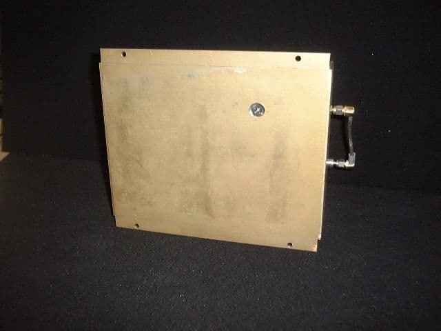
MKRU519
Mar 05, 20019 Antenna InstaScan Scanner, Model U519
Equipment Class
DSS - Part 15 Spread Spectrum Transmitter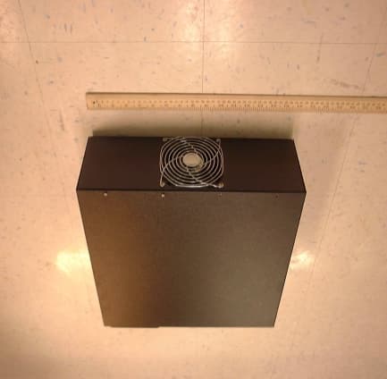
MKRS556
May 22, 2000Model S556 Scanner
Equipment Class
TNB - Licensed Non-Broadcast Station Transmitter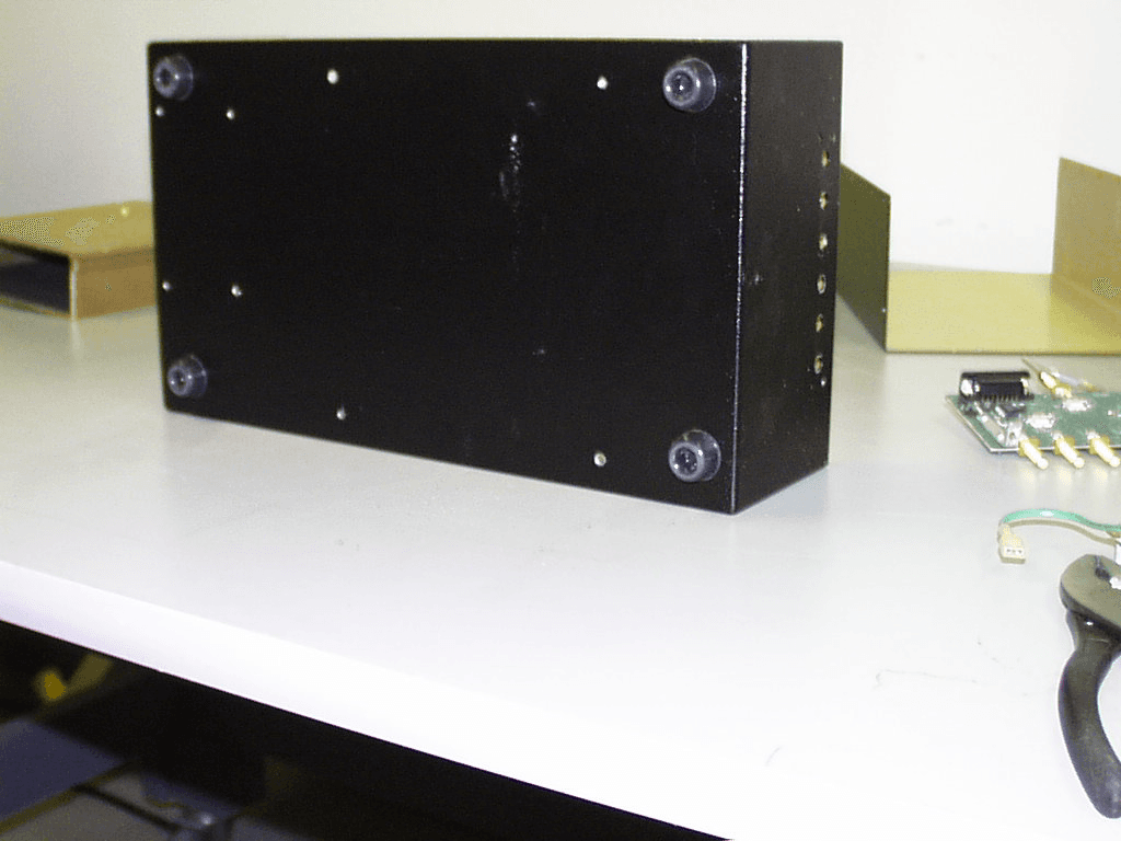
MKRS516
May 07, 20006 Antenna InstaScan Scanner
Equipment Class
DSS - Part 15 Spread Spectrum Transmitter