NCBSL9102Spread Spectrum Transmitter
Wave Wireless Networking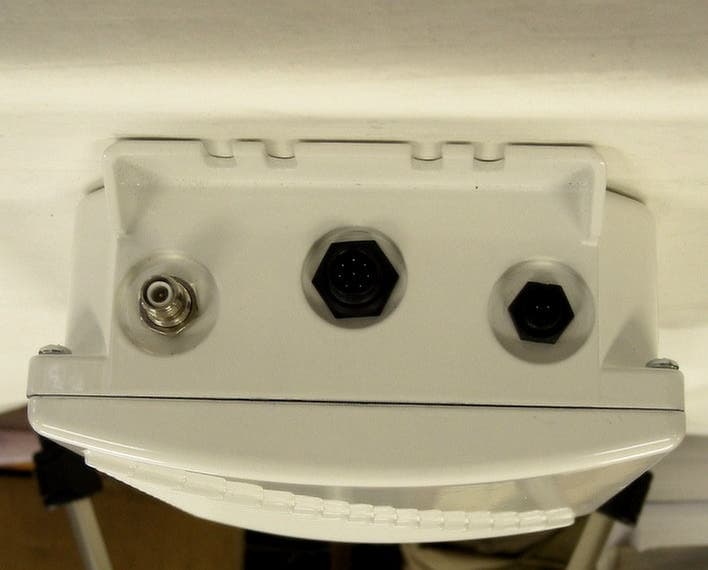
Click to zoom
Application Details
- Equipment Class
- DTS - Digital Transmission System
- Date of Grant
- May 08, 2002
- Application Purpose
- Original Equipment
- Date of Application
- May 08, 2002
- Equipment Note
- Spread Spectrum Transmitter
- Frequency Range
- 2412.00000000 - 2462.00000000
- Company
- Wave Wireless Networking
- Country
- United States
Documents & Files
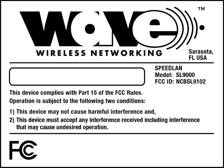
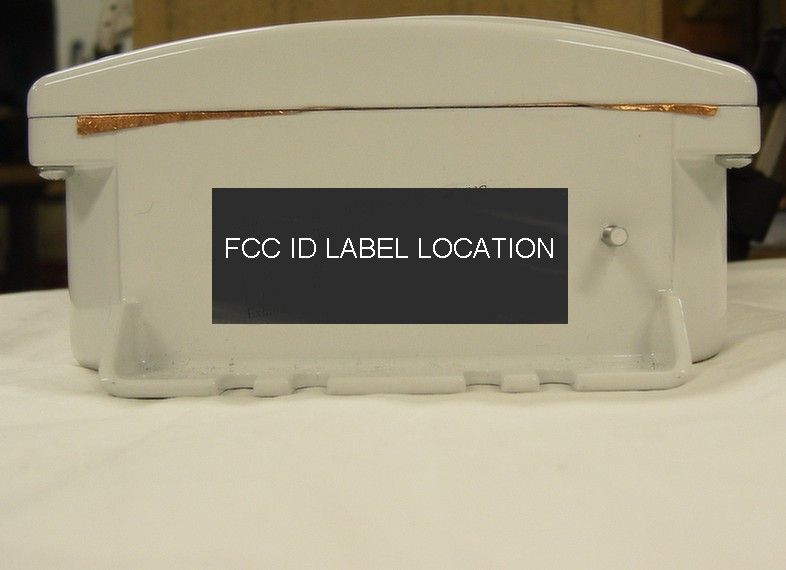
Document Text
Text extracted from the exhibit documents filed with the FCC. Open a document above to read the original.
Users Manual
A S P E E D C O M W I R E L E S S C O R P O R AT I O N S P E E D L A N 9 0 0 0 SPEEDLAN 9000 Series Installation and Operation User Guide Version 1.0 Last Revised: March 2002 SPEEDLAN 4100 & 4200 Installation and Operation User Guide -2 Copyright/Liability Copyright ©2002. Wave Wireless Networking. All rights reserved. SPEEDLAN and SPEEDCOM are registered trademarks of Wave Wireless Networking. SPEEDView, Wave Wireless Networking and the Wave Wireless Networking logo are trade- marks of Wave Wireless Networking. All other trademarks mentioned in this document are the property of their respective owners. Contents of this publication may be preliminary and/or may be changed at any time without notice and shall not be regarded as a warranty. For more information, contact Wave Wireless Networking at: Wave Wireless Networking 7020 Professional Parkway East Sarasota, FL 34240 www.wavewireless.com Technical Support 941-907-2300 (phone) 941-355-0219 (fax) SPEEDLAN 9000 Series Installation and Operation User Guide Contents-1 Chapter 1 - Introduction ............................................................................... 1-1 Features and Benefits ................................................................................................................ 1-2 SPEEDLAN 9000 Series Features......................................................................................... 1-2 ISP Functionality ................................................................................................................ 1-2 Configuration and Monitoring ............................................................................................ 1-3 Wired LAN Interface........................................................................................................... 1-3 Wireless LAN Interface ....................................................................................................... 1-3 SPEEDView (A Network Management Tool) .......................................................................... 1-4 IP-Router Features ............................................................................................................. 1-4 Additional Functionality for SPEEDLAN 9000 RF cable loss is negligible ................................. 1-4 Equipment Features................................................................................................................... 1-4 SPEEDLAN K2's Polling Protocol -- How it Works in Star Networks ................................................. 1-5 Point-to-Multipoint Functionality .......................................................................................... 1-5 Point-to-Point Functionality ................................................................................................. 1-7 SPEEDLAN 9000 Mesh Protocol -- How It Works in Non-Line-of-Sight Networks............................. 1-8 Routing Around Obstacles................................................................................................ 1-10 SPEEDLAN’s NLOS Pico Cell Architecture .......................................................................... 1-11 SPEEDLAN 9000 Mesh Protocol's Core Components .......................................................... 1-11 Network Expansion: Connecting Buildings in a SPEEDLAN 9000 Network ............................ 1-12 Chapter 2 - Installing the SPEEDLAN 9101 & SPEEDLAN 9102 Hardware........................................................................................................ 2-1 Rooftop and Tower Installations Warning .................................................................................... 2-2 Hardware Overview .................................................................................................................. 2-2 Drawings of Outdoor, Remote-Mounted Components .................................................................. 2-2 Indoor Junction Box ........................................................................................................... 2-2 The SPEEDLAN 9101 (with an Attached Standard Omni) .............................................................. 2-3 Bottom View of SPEEDLAN 9101 ....................................................................................... 2-3 System Description............................................................................................................. 2-4 Package Contents............................................................................................................. 2-4 Installation Steps for the SPEEDLAN 9101............................................................................ 2-5 Installation Diagram of the SPEEDLAN 9101........................................................................ 2-6 The SPEEDLAN 9102 (with an External Antenna) .......................................................................... 2-8 Bottom View of SPEEDLAN 9102 ..................................................................................... 2-11 System Description............................................................................................................. 2-1 Package Contents............................................................................................................ 2-11 Installation Steps for the SPEEDLAN 9102.......................................................................... 2-12 Installation Diagram of the SPEEDLAN 9102...................................................................... 2-17 Chapter 3 - Using the SPEEDLAN 9000 Configurator............................... 3-1 Initial Configuration of the SPEEDLAN 9000 ................................................................................3-2 Prerequisites ......................................................................................................................3-2 Configuring the SPEEDLAN 9000.......................................................................................…
Text truncated - open the document above for the full version.
Block Diagram
U11 Ethernet MAC/PHY National Semiconductor DP83815 U10 Buffer, hex 74LVC125 U14 Serial EEPROM 93C46 U2 SDRAM 16M x 16 U3 SDRAM 16M x 16 U17 RS-232 Transceiver MAX3243 (not used) X1 Crystal 32 MHz X2 Crystal 32.768 kHz U4 Flash Memory 128k x 8 SST 39VF010 U6 DC/DC Converter MAX1714 P1 Connector 9-pin D-sub X3 Crystal Oscillator 25 MHz U13 Ethernet MAC/PHY National Semiconductor DP83815 U15 Ethernet MAC/PHY National Semiconductor DP83815 U16 Serial EEPROM 93C46 U12 Serial EEPROM 93C46 T1 Ethernet Transformer & Filter T2 Ethernet Transformer & Filter T3 Ethernet Transformer & Filter U5 RS-232 Transceiver MAX3243 J1 Connector DC Power Input JP7 Modular Jack 8-position JP8 Modular Jack 8-position JP6 Modular Jack 8-position Q3 Dual FET IR147 BT1 Battery J2 Connector PCI Bus J3 Connector mini PCI JP2 Connector Compact Flash JP3 Connector Alt. Power U8 Voltage Regulator D3,6,10 LEDs JP1 Connector JTAG Debugger JP11 Connector 10-pin header (not used) JP3 Connector Parallel I/O PCI Bus Local Bus Controller SDRAM Bus Controller U1 MicroProcessor AMD Elan SC520 PCI Bus Controller UART1 UART2 JTAG Port MAC/PHY GPIO Real Time Clock Clock Gen Block Diagram: Soekris net4501 Single Board Computer
Cover Letter(s)
January 7, 2002 Federal Communications Commission Authorization and Evaluation Division 7435 Oakland Mills Road Columbia, MD 21046 RE: Confidentiality Request regarding application for certification of WAVE WIRELESS NETWORKING, FCC Certification of FCC ID: NCBSL9102 To Whom It May Concern: Pursuant to Sections 0.457 and 0.459 of the Commission’s Rules, we hereby request confidential treatment of information accompanying this application as outlined below: Schematics The above materials contain trade secrets and proprietary information not customarily released to the public. The public disclosure of these materials may be harmful to the applicant and provide unjustified benefits to its competitors. The applicant understands that pursuant to Section 0.457 of the Rules, disclosure of this application and all accompanying documentation will not be made before the date of the Grant for this application. Sincerely, Janusz Dyndul Product Certification Manager WAVE WIRELESS NETWORKING 941-358-9283 ext. 407 [email protected]
External Photos
WAVE WIRELESS NETWORKING FCC ID: NCBSL9102 EXTERNAL PHOTOGRAPHS TOP VIEW EXTERNAL PHOTO BOTTOM VIEW EXTERNAL PHOTO EXTERNAL REAR VIEW PHOTO
External Photos
Page 1 ANNEX PHOTOGRAPHS OF EUT
Internal Photos
Page 2 Page 3
Internal Photos
Page 4 Page 5
Operational Description
Operational description. Product overview This product is a Ethernet to RF transceiver. The product consists of a custom IBM compatible single board computer with a network interface controller card(NIC) and a radio transceiver installed in a PCMIA port card. The RF card: This device is Direct Sequence Spread Spectrum, the data is mixed by pseudorandom code which is an orthogonal code. The mixed data is digital modulated by BPSK and QPSK technique depends on the data rates. The CCK coding is applied fro increasing the data rate, and also the processing gain will be increased. The bit rates are 1,2,5.5, 11Mbps, the symbol rates are 1,1,1.375,1.375Mbps, the chip rates are always 11Mbps. So, the Chip/symbol is 11,11,8 and 8 respectively. Although is higher bit rate, the processing gain is lower than 10, but the CCK coding used in higher bit rate will provide 2.2dB coding gain. The oscillators employed are a VCO from 2030 to 2090MHz controlled by software, 704 MHz, and which when divided by 2 gives the 352 MHz an IF local oscillator. The computer: The CPU uses 25 and 32MHz crystal oscillators.
Test Report
APPLICANT: WAVE WIRELESS NETWORKING FCC ID: NCBSL9102 REPORT #: T:\W\Wave_NCB\241aut2\241AUT2TestReport.doc TABLE OF CONTENTS LIST APPLICANT: WAVE WIRELESS NETWORKING FCC ID: NCBSL9102 TABLE OF CONTENTS TEST REPORT CONTAINING: PAGE 1.............LETTER REQUESTING CONFIDENTIALLY AND LETTER OF EXPLANATION PAGE 2-5...........LIST OF TEST EQUIPMENT PAGE 6.............TEST PROCEDURES PAGE 7.............PRODUCT DESCRIPTION PAGE 8.............POWERLINE CONDUCTED INTERFERENCE PAGE 9-10..........POWERLINE CONDUCTED PLOTS PAGE 11.............OCCUPIED BANDWIDTH AND POWER OUTPUT PAGE 12.............6 dB BANDWIDTH PLOT PAGE 13.............METHOD OF MEASURING RF CONDUCTED AND SPURIOUS EMISSIONS AT ANTENNA TERMINALS DATA PAGE 14.............RADIATION INTERFERENCE TEST DATA PAGE 15.............METHOD OF MEASURING RADIATED SPURIOUS EMISS. PAGE 16.............RADIATED SPURIOUS EMISSIONS INTO ADJACENT RESTRICTED BANDS PAGE 17.............POWER SPECTRAL DENSITY PAGE 18.............POWER SPECTRAL DENSITY PLOT PAGE 19.............BANDEDGE PLOT PAGE 20.............MPE CALCULATIONS EXHIBIT ATTACHMENTS: EXHIBIT 1...........REQUEST FOR CONFIDENTIALITY LETTER EXHIBIT 2...........FCC ID LABEL SAMPLE EXHIBIT 3...........SKETCH OF FCC ID LABEL LOCATION EXHIBIT 4...........EXTERNAL PHOTOS EXHIBIT 5...........INTERNAL PHOTOS EXHIBIT 6...........PHOTOGRAPHS – Z-COM RADIO EXHIBIT 7...........BLOCK DIAGRAM EXHIBIT 8...........TEST SETUP UP PHOTOGRAPHS EXHIBIT 9...........BLOCK DIAGRAM – CPU BOARD EXHIBIT 10..........SCHEMATICS – Z COM RADIO EXHIBIT 11..........SCHEMATICS – POWER SUPPLY BOARD EXHIBIT 12..........PROCESSING GAIN TEST DATA EXHIBIT 13..........OPERATIONAL DESCRIPTION EXHIBIT 14..........USER’S MANUAL APPLICANT: WAVE WIRELESS NETWORKING FCC ID: NCBSL9102 REPORT #: T:\W\Wave_NCB\241aut2\241AUT2TestReport.doc Page 1 of 20 MAY 1, 2002 Federal Communications Commission Authorization and Evaluation Division 7435 Oakland Mills Road Columbia, MD 21046 SUBJECT: WAVE WIRELESS NETWORKING FCC ID: NCBSL9102 To Whom It May Concern: The attached application is for a direct sequence spread spectrum assembly, made up of the Bridge/Radio (FCC ID: M4Y-06250), 50 foot of coax, a lightning arrestor, and a parabolic antenna. This system has only one type of antenna, a parabolic grill type that has a gain of 24dBi. WAVE WIRELESS NETWORKING purchases standard antennas from the manufacturer. The antenna is intended to be used outside and fixed mounted to a permanent structure. The NCBSL9102 radio uses unique connector (reverse TNC). The unit is designed to be professionally installed. Should you have any questions or require any further information with regards to this, please feel free to contact me. Sincerely, Mario R. de Aranzeta Engineer MRD/sh Encl. APPLICANT: WAVE WIRELESS NETWORKING FCC ID: NCBSL9102 REPORT #: T:\W\Wave_NCB\241aut2\241AUT2TestReport.doc Page 2 of 20 Equipment List DEVICE MFGR MODEL SERNO CAL/CHAR DATE DUE DATE or STATUS X 3-Meter OATS TEI N/A N/A Listed 12/22/99 12/22/02 3/10-Meter OATS TEI N/A N/A Listed 3/26/01 3/26/04 X Receiver, Beige Tower X Spectrum Analyzer (Tan) HP 8566B Opt 462 3138A07786 3144A20661 CAL 8/31/01 8/31/02 X RF Preselector (Tan) HP 85685A 3221A01400 CAL 8/31/01 8/31/02 X Quasi-Peak Adapter (Tan) HP 85650A 3303A01690 CAL 8/31/01 8/31/02 Receiver, Blue Tower Spectrum Analyzer (Blue) HP 8568B 2928A04729 2848A18049 CHAR 10/22/01 10/22/02 RF Preselector (Blue) HP 85685A 2926A00983 CHAR 10/22/01 10/22/02 Quasi-Peak Adapter (Blue) HP 85650A 2811A01279 CHAR 10/22/01 10/22/02 Biconnical Antenna Electro-Metrics BIA-25 1171 CAL 4/26/01 4/26/03 X Biconnical Antenna Eaton 94455-1 1096 CAL 10/1/01 10/1/02 Biconnical Antenna Eaton 94455-1 1057 CHAR 3/15/00 3/15/01 BiconiLog Antenna EMCO 3143 9409-1043 X Log-Periodic Antenna Electro-Metrics LPA-25 1122 CAL 10/2/01 10/2/02 Log-Periodic Antenna Electro-Metrics EM-6950 632 CHAR 10/15/01 10/15/02 Log-Periodic Antenna Electro-Metrics LPA-30 409 CHAR 10/16/01 10/16/02 Dipole Antenna Kit Electro-Metrics TDA-30/1-4 152 CAL 3/21/01 3/21/02 Dipole Antenna Kit Electro-Metrics TDA-30/1-4 153 CHAR 11/24/00 11/24/01 X Double-Ridged Horn Antenna Electro-Metrics RGA-180 2319 CAL 12/19/01 12/19/02 Horn Antenna Electro-Metrics EM-6961 6246 CAL 3/21/01 3/21/02 Horn Antenna ATM 19-443-6R None No Cal Required Passive Loop Antenna EMC Test Systems EMCO 6512 9706-1211 CHAR 7/10/01 7/10/02 Line Impedance Stabilization . . . Electro-Metrics ANS-25/2 2604 CAL 10/9/01 10/9/02 APPLICANT: WAVE WIRELESS NETWORKING FCC ID: NCBSL9102 REPORT #: T:\W\Wave_NCB\241aut2\241AUT2TestReport.doc Page 3 of 20 DEVICE MFGR MODEL SERNO CAL/CHAR DATE DUE DATE or STATUS X Line Impedance Stabilization . . . Electro-Metrics EM-7820 2682 CAL 3/16/01 3/16/02 Termaline Wattmeter Bird Electronic Corporation 611 16405 CAL 5/25/99 (5/25/00) Termaline Wattmeter Bird Electronic Corporation 6104 1926 CAL 12/12/01 12/12/02 Oscilloscope Tektronix 2230 300572 CHAR 2/1/01 2/1/02 Temperature Chamber Tenney Engineering TTRC 11717-7 CHAR 1/22/02 1/22/03 AC Voltmeter HP 400FL 2213A14499 CAL 10/9/01 10/9/02 AC Voltmeter HP 400FL 2213A14261 CHAR 10/15/01 10/15/02 AC Voltmeter HP 400FL 2213A14728 CHAR 10/15/01 10/15/02 X Digital Multimeter Fluke 77 35053830 CHAR 1/8/02 1/8/03 Digital Multimeter Fluke 77 43850817 CHAR 1/8/02 1/8/03 Digital Multimeter HP E2377A 2927J05849 CHAR 1/8/02 1/8/03 Multimeter Fluke FLUKE-77-3 79510405 CAL 9/26/01 9/26/02 Peak Power Meter HP 8900C 2131A00545 CHAR 1/26/01 1/26/02 Digital Thermometer Fluke 2166A 42032 CAL 1/16/02 1/16/03 Thermometer Traulsen SK-128 CHAR 1/22/02 1/22/03 Temp/Humidity gauge EXTech 44577F E000901 CHAR 1/22/02 1/22/03 Frequency Counter HP 5352B 2632A00165 CAL 11/28/01 11/28/02 Power Sensor Agilent Technologies 84811A 2551A02705 CAL 1/26/01 1/26/02 Injection Probe Fischer Custom Communications F-120-9A 270 CAL 6/1/01 6/1/02 Service Monitor IFR FM/AM 500A 5182 CAL 11/22/00 11/22/01 Comm. Serv. Monitor IFR FM/AM 1200S 6593 CAL 11/12/99 11/12/00 Signal Generator HP 8640B 2308…
Text truncated - open the document above for the full version.
Test Report
Confidential Page1 Processing Gain of Direct Sequence Spread Spectrum Product name: XI-625 Wireless LAN Mini PCI Card Tested by: Z-Com, Inc. Prepared by: H.S.Chung, Hardware Engineer TEL: (886)-3-3577364 ext.146 FAX: (886)-3-5773359 Email: [email protected] Date: JAN. 18, 2002 FCC requirements: The processing gain of a direct sequence system shall be at least 10dB. The processing gain shall be determined from the ratio in dB of the signal-to-noise ratio with the system spreading code turned off to the signal-to-noise ratio with the system spreading code turned on, as measured at the demodulated output of the receiver. This document contains theoretical calculation and test setup, procedure, measurement data and report. Test equipment: R&S FSEM20 spectrum analyzer R&S SMIQ03B signal generator Giga-tronics 8541C universal power meter Hp8496B attenuator/110dB with 10dB step Hp8494B attenuator/11dB with 1dB step Hp11636BB power splitter Desktop PC Notebook PC Theoretical calculation: The Processing gain is related to be jamming margin as follows: Where BER reference is the reference bit error ratio with its corresponding, theoretical output signal to noise ratio per symbol, (S/N) output , (J/S) is the jamming margin(jamming signal power relative to desired signal power), and L sys is the system losses. Confidential Page2 For 5.5Mbps and 11Mbps case: The HFA3861B direct sequence spread spectrum baseband processor use CCK modulation which is a form of M-ary Orthogonal Keying. The Probability of error for generalized M-ary orthogonal signaling using coherent demodulation is given by: The FER performance curve is derived by [1] as left graph: Therefore: Gp = (Es/No)o + (J/S) + Lsys =16.4 + 2.0 + (J/S) and, Gp = 18.4 + (J/S) must be greater than 10dB For the case of the HFA3861B, the bit rates are 1,2, 5.5 and 11Mbps. The corresponding symbol rates are 1, 1, 1.375 and 1.375 Msps. The chip rate is always 11Mcps, so the ratio of chip rate to symbol rate is 11:1 for the 1, 2Mbps and 8:1 for 5.5, 11Mbps rates. Since the symbol rate to bit rate is less than 10 for the higher rates, we supply the theoretical processing gain and coding are utilized. This is a reasonable in that they cannot be separated in the demodulation process. If a separable FEC coding scheme were used, we would not be comfortable making this assertion. As can be seen from the curve of figure 1, the Es/No is 16.4dB at the PER of 8%. It is well know that the Eb/No of BPSK is 9.6dB for 1e-5 BER, so therefore the coding gain of CCK over BPSK is 2.2dB. We add this to the processing gain of 9B to get 11.2dB overall processing gain for the CW jamming test. 15.51616.517 10 -2 10 -1 10 0 11 Mbps CCK in Thermal Noise Es/No (dB) 1000 byte Packet Error Rate Confidential Page3 Taking the calculation above, if the (J/S)>-8.4dB then the equipment passes the CW jamming test. For 1 and 2Mbps case, the modulation is either DBPSK or DQPSK for 1 and 2Mbps. With differential coding, there is an error extension factor of 2 which comes from the fact that if one symbol is error, then the next will be demodulated in error too. Since its phase is dependant on the change of phase from symbol to symbol. In DBPSK, this result is a simple factor of two in BER. With DQPSK, the picture is a little muddied in that a symbol error may cause one or two bit errors since two bits are carried per symbol. From the book of Fig.7.2, Viterbi, A.J. Principles of Coherent Communications, Page 192 (New York; McGraw-Hill, 1996), the Eb/No of BPSK is 9.6dB. When operating DQPSK at 2Mbps, the Eb/No remains essentially the same, but the Es/No goes up by 3dB. So the (S/N)o is 12.6. Test procedure: Obtain the simplex link shown. Perform all independent instrumentation calibration prior to this procedure. Set operating levels using fixed and variable attenuator in system to meet the following objectives: 1. Signal Power at receiver is approximately –60dBm. 2. Signal Power at power meter between –20 and –30dBm. 3. Use spectrum analyzer to monitor test. 4. Ensure that CW jammer generator RF output is disabled and measure the power at the power meter port using Giga-tronics 8541C power meter. This is relative power, Sr. 5. Disable TX and set CW jammer output frequency equal to the carrier frequency and enable generator output. Set reference CW jammer power level at power meter port 8.4dB below Sr. 6. Disable CW jammer and re-establish Link. FER test should be essentially error free. 7. Enable the CW jammer at the reference power level and verify that FER at the reference power level and verify that FER test indicate less than 8%. 8. Alternatively, adjust the CW jammer level to that which causes 8% FER. 9. Repeat Step 7 for uniform steps in frequency increments of 50KHz across the receiver passband with the CW jammer. In this case, the receiver passband is 8.5MHz Test setup: as shown at next page Confidential Page4 Processing gain test result summary: Frequency channel Frequency Data rate (Mbps) Gp (dB) 1 2412MHz 11 11.1 6 2437MHz 11 10.7 11 2462MHz 11 11.4 Notebook Access Point Power Combiner SG R&SIQ03 Desktop PC XI-625 Mini PCI Card Step Attenuator(30dB)Power Splitter Power splitter Spectrum analyzer R&S SFEM20 Power meter Gigatronic 8541C Shielding room 20dB Attenuator Processing gain test setup
Test Setup Photos
WAVE WIRELESS NETWORKING FCC ID: NCBSL9102 RADIATED EMISSIONS TEST SET UP PHOTO POWERLINE CONDUCTED EMISSIONS TEST SET UP
Contact Information
Applicant
John Dyndul(Product Certification Manager)
Test Firm
Timco Engineering, Inc.S Sanders
Technical Specifications
| # | Rule Parts | Frequency Range | Power Output |
|---|---|---|---|
| 1 | 15C | 2.41 GHz - 2.46 GHz | 21.00 mW |
Other Applications from Wave Wireless Networking
NCBSL9101A
Dec 11, 2003Spread Spectrum Transmitter
Equipment Class
DTS - Digital Transmission System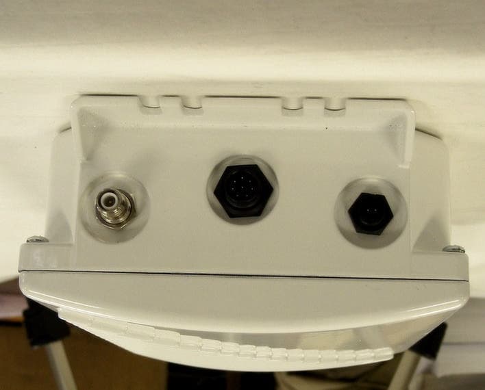
NCBSL9102A
Dec 09, 2003SPREAD SPECTRUM TRANSMITTER
Equipment Class
DTS - Digital Transmission System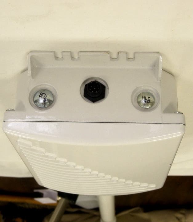
NCBSL9101
May 06, 2002Spread Spectrum Transmitter
Equipment Class
DTS - Digital Transmission System
NCBSLXE2
Apr 11, 2002Spread Spectrum Transmitter
Equipment Class
DSS - Part 15 Spread Spectrum Transmitter
NCBSL8500
Mar 31, 2002Spread Spectrum Transmitter
Equipment Class
DSS - Part 15 Spread Spectrum Transmitter