NCBSLXE
Wave Wireless Networking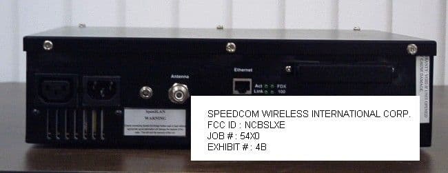
Click to zoom
Application Details
- Equipment Class
- DSS - Part 15 Spread Spectrum Transmitter
- Date of Grant
- Sep 10, 2000
- Application Purpose
- Original Equipment
- Date of Application
- Apr 27, 2000
- Frequency Range
- 2421.10000000 - 2422.10000000
- Company
- Wave Wireless Networking
- Country
- United States
Documents & Files
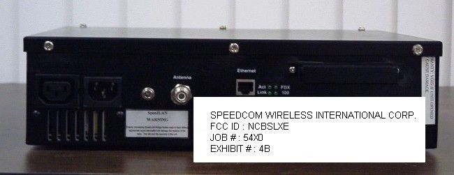
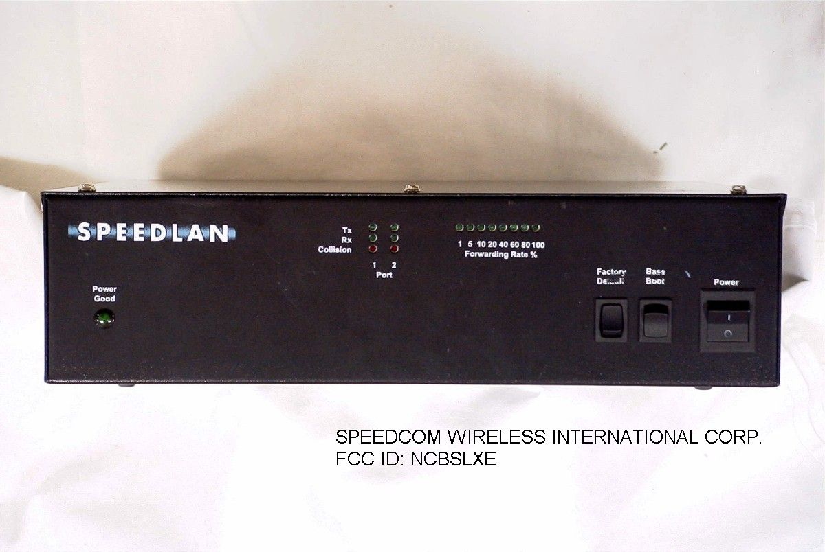
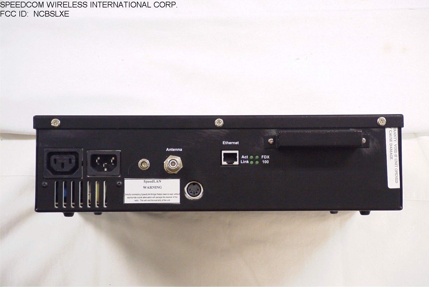
Document Text
Text extracted from the exhibit documents filed with the FCC. Open a document above to read the original.
Users Manual
SPEEDLAN 4100 & 4200 4 Limitation of Warranty The foregoing warranty shall not apply to defects resulting from improper or inadequate maintenance by the buyer, buyer supplied interfacing, unauthorized modification or misuse, operation outside of the environmental specifications for the product, or improper site preparation or maintenance. Systems must be protected from electrical brownouts and surges by a quality UPS such as an APC Smart brand or Tripp Lite Omni or similar, or warranty shall be null and void. Warranties do not apply to any product that has been (i) altered, except expressly approved by Wave Wireless in accordance with its instructions, (ii) damaged by improper electrical power or environment, abuse, misuse, accident, or negligence. Repairs in the case of damage from “acts of God” are covered on a time and materials basis. The warranty shall not apply if Wave Wireless prebuilt U.S. FCC approved antenna assemblies have been altered and installed by any persons other than professional wireless installers. THE FOREGOING WARRANTIES ARE EXCLUSIVE REMEDIES AND ARE IN LIEU OF ALL OTHER WARRANTIES, EXPRESS OR IMPLIED, INCLUDING, WITHOUT LIMITATION, ANY WARRANTY OF MERCHANTABILITY OR FITNESS FOR A PARTICULAR PURPOSE. No statement, including, without limitation, representations regarding capacity, suitability for use or performance of products, whether made by Wave Wireless employees or otherwise, shall be deemed to be a warranty by Wave Wireless for any purpose or give rise to any liability for Wave Wireless unless expressly contained in writing. Resellers will have complete responsibility and liability for performance of its agreements with its customers and Resellers shall indemnify and hold Wave Wireless harmless from and against all liability arising out of such agreements. Wave Wireless warrants that the firmware for use with the unit will execute its programming instructions when properly installed on the unit. Wave Wireless does not warrant that the operation of the unit or firmware will be uninterrupted or error-free. Wave Wireless shall not be obligated to remedy any software defect that cannot be repeated. Wave Wireless is not responsible for equipment non-performance due to outside radio interference caused by any source. Exclusive Remedies The remedies provided herein are the buyer’s sole and exclusive remedies. Wave Wireless shall not be liable for any direct, indirect, special, incidental or consequential damages, whether based on contract, tort or any legal theory. OTHER IMPORTANT STATEMENTS AND WARNINGS Copyright/Liability SPEEDLAN 4100 & 4200. Copyright ©1999/2000.Wave Wireless Networking, a SPEEDCOM Wireless Company. All rights reserved. No part of this publication may be reproduced, transmitted, transcribed, stored in a retrieval system, or translated into any language in any form by any means without the written permission Wave Wireless, a SPEEDCOM Wireless Company Wave Wireless Networking, a SPEEDCOM Wireless Company, shall not be liable for errors contained herein or for incidental or consequential damages in connection with the furnishing, performance, or use of this material. Wave Wireless Networking, a SPEEDCOM Wireless Compnay, reserves the right to revise this publication from time to time and make changes in content without obligation to notify any person of such revision changes. Contents of this publication may be preliminary and/or may be changed at any time without notice and shall not be regarded as a warranty. Trademarks Wave Wireless Networking’s name and all trademarks in this document are property of SPEEDCOM Wireless, except for Microsoft® Corporation Windows 95®, Windows 98®, and Windows NT®. FCC STATEMENT (FOR USA ONLY) FEDERAL COMMUNICATIONS COMMISSION Radio Frequency Interference Statement for Spread Spectrum Devices Warning: This equipment generates, uses, and can radiate radio frequency energy. If it is not installed and used in accordance with the instruction manual, it may cause interference to radio communications. It has been tested and found to comply with the limits for a Class A computing device pursuant to Part 15 of FCC Rules, which are designed to provide reasonable protection against such interference when operated in a commercial environment. Operation of this equipment in a residential area will probably cause interference, in which case the user at his own expense will be required to take whatever measures may be required to correct the interference. Electronic Emission Notices All the spread spectrum devices sold in this catalog comply with Part 15 of the FCC rules. Operation is subject to the following two conditions: 1.This device may not cause harmful interference. 2.This device must accept any interference received, including interference that may cause undesired operation. If this equipment causes interference to radio reception (which can be determined by unplugging the power cord from the equipment) try these measures: (1) Re-orient the receiving antenna, (2) Relocate the equipment with respect to the receiver, (3) Plug the equipment and receiver into different branch circuits, or (4) Consult your dealer or an experienced technician for additional suggestions. DANGER!!! Rooftop or tower antenna installations are extremely dangerous and incorrect installation may result in injury, damage, or death. Rooftop and tower installations must be performed by professional antenna installers only. WARNING! This is a 2.4 GHz point-to-point system. The conducted output is 36mW with Gant = 24 dBi. This system is used exclusively for fixed point-to-point operations. It is prohibited to transmit the same information from multiple co-located antennas. This equipment must be professionally installed. In order to comply with FCC RF Exposure requirements, this device must be installed in such that a minimum separation distance of 1 meter (3.5’) is always maintained between the antenna and all persons. The operator and professional inst…
Text truncated - open the document above for the full version.
Cover Letter(s)
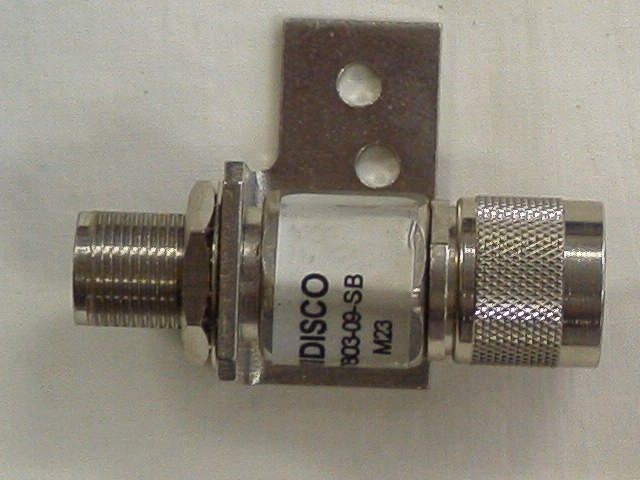
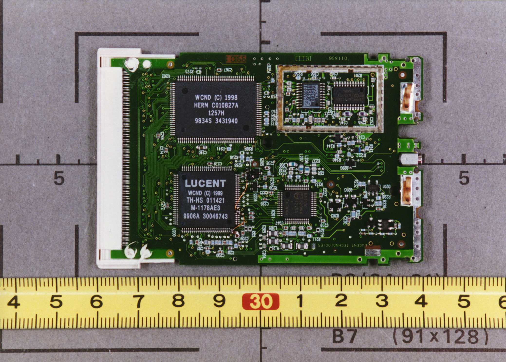
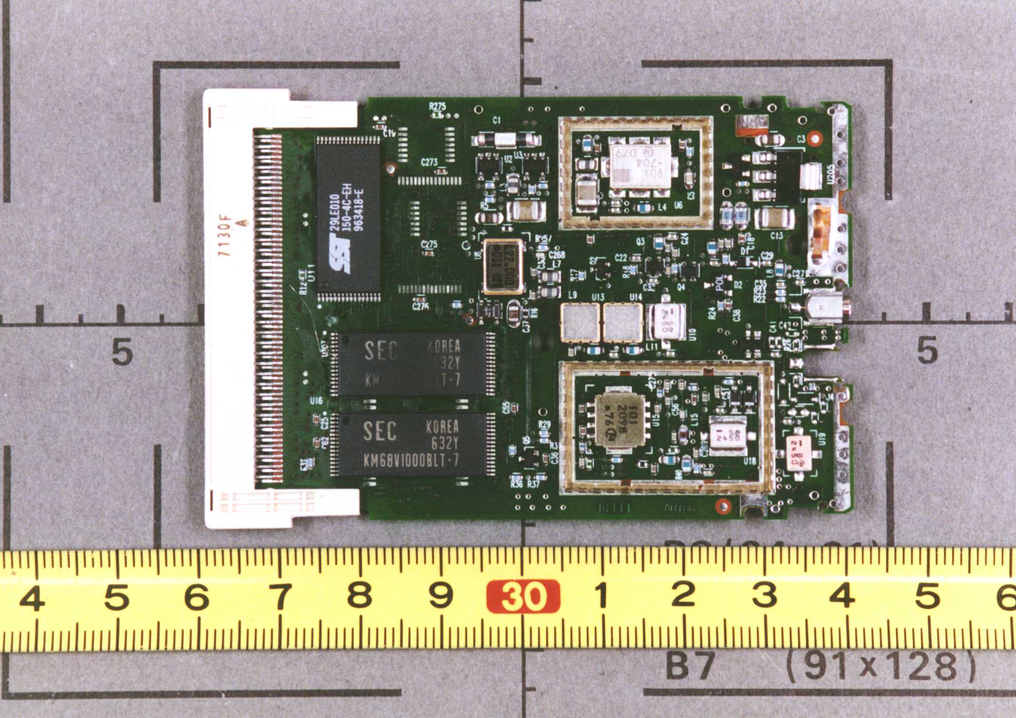
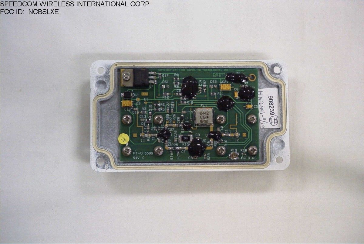
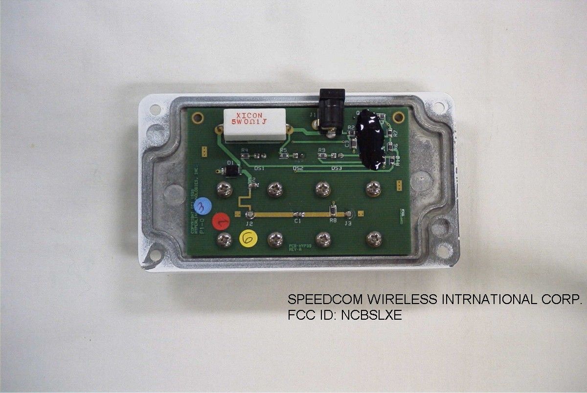
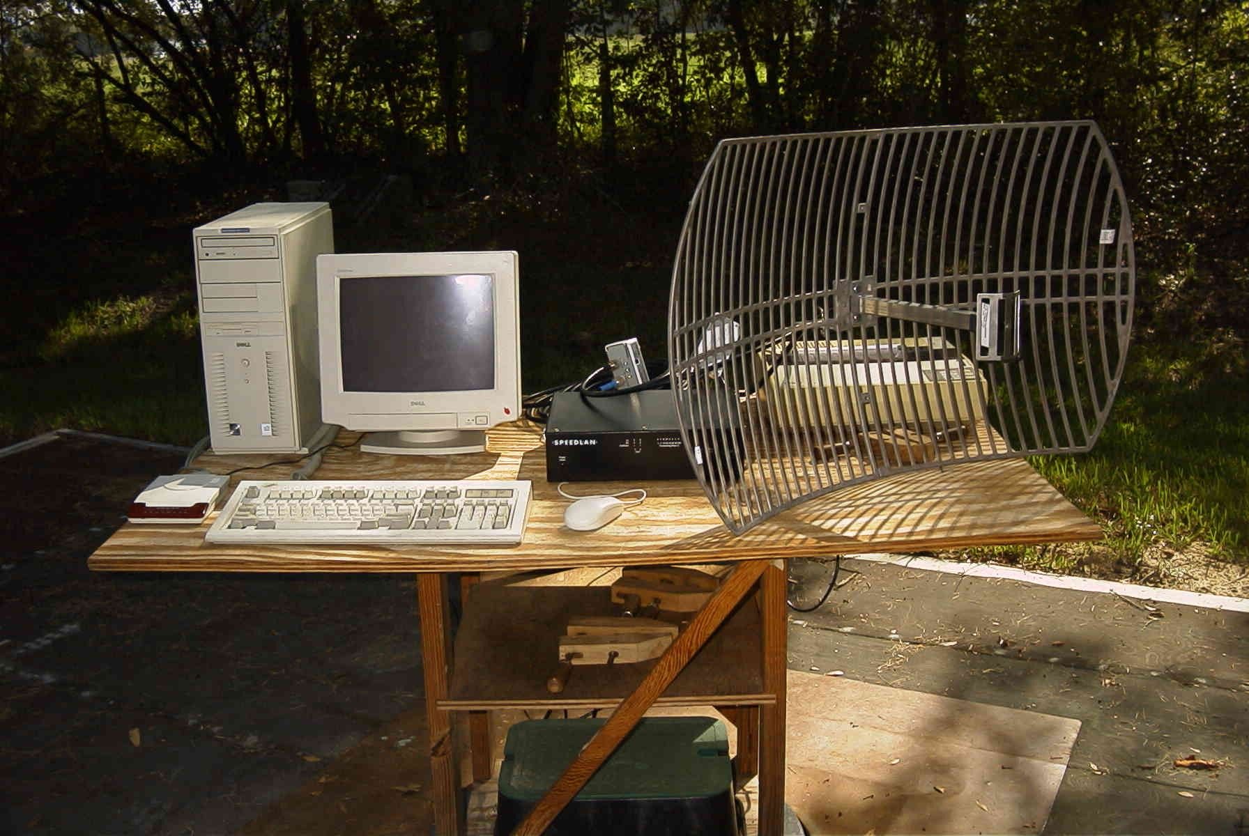
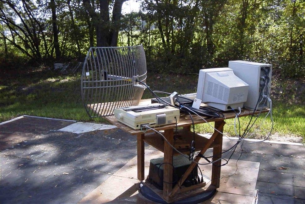
849 NW State Road 45 • P. O. Box 370 • Newberr y, Florida 32669 USA Telephone (352) 472-5500 • (888) 472-2424 • FAX (352) 472-2030 • email: [email protected] August 2, 2000 Mr. Joe Dichoso Federal Communications Commission Authorization and Evaluation Division 7435 Oakland Mills Road Columbia, MD 21046 Ref: Speedcom Wireless International Corp.’s FCC ID: NCBSLXE Confirmation #: EA97480, Correspondence ID #: 14431 Dear Joe: 1. I have uploaded better external photos. 2. A. I have uploaded internal and external photos of the amplifier. B. I have uploaded a photograph of the lightning arrestor. C. The schematics of the amplifier will be sent to you from the manufacturer. D. The test data that you have that was originally sent with the report is with the amplifier in place and turned on. Since the amplifier was an integral part of the test configuration, I don’t believe you will need additional radiated and conducted test data. If I am incorrect, please advise. 3. The schematics will be sent to you from the manufacturer. 4. The processing gain information will be sent to you from the manufacturer. 5. The connectors are reverse polarity TNC connectors. The professional installation information for the manual has been uploaded. 6. The photos of both side of the transceiver board with the shielded removed will be sent to you by the manufacturer. 7. I have uploaded the test set up photos. 8. I have uploaded the portion of the manual that has the point-to-point language as specified in Section 15.247(b)(3)(iii). If you require any further information, please advise. Regards, Sharon Hoffman/TIMCO ENGINEERING, INC.
Cover Letter(s)
849 NW State Road 45 • P. O. Box 370 • Newberr y, Florida 32669 USA Telephone (352) 472-5500 • (888) 472-2424 • FAX (352) 472-2030 • email: [email protected] August 11, 2000 Mr. Joe Dichoso Federal Communications Commission Authorization and Evaluation Division 7435 Oakland Mills Road Columbia, MD 21046 Ref: Speedcom Wireless International Corp.’s FCC ID: NCBSLXE Confirmation #: EA97480, Correspondence ID #: 15438 Dear Joe: 1. The schematics of the amplifier are being sent from Hyperlink. 2. Sheet 1 of the schematic of the radio is being sent from Lucent. 3. The processing gain information is being sent from Lucent. 4. The photos of the transceiver board without shielding is being sent from Lucent. 5. I have sent a revised Page 4 of the user’s manual which should cover the point-to- point installation instructions. 6. I have sent test set up photos and data. 7. I have sent the confidential letter. If you have any questions or require any further information, please advise. Regards, Sharon Hoffman/TIMCO ENGINEERING, INC.
Cover Letter(s)
August 9, 2000 Federal Communicatio ns Co mmission Authorization and Evaluation Division 7435 Oakland Mills Road Columbia, Maryland 21046 Subject: Speedcom Wireless International Corp., FCC ID: NCBSLXE , Conf.No. EA 97480 Correspondence Ref. No.15438. To Whom It May Concern: This will serve as a request for confidentiality for the schematics for the radio and amplifier. The schematics will be sent directly from the manufacturers to the FCC upon Request. Once the review of the application is complete and the schematics are no longer needed, they must be returned to the manufacturer, where they were sent from. Should you have any questions or require any further information with regards to this, please feel free to contact me. Sincerely, William Gamin Development Coordinator Wave Wireless Networking 941-358-9283 ext. 318 [email protected]
Cover Letter(s)
1201 Clint Moore Road Boca Raton, FL 33487 USA Tel: 561-995-2256 Fax: 561-995-2432 Mr. Joe Dichoso Federal Communications Commission Authorization and Evaluation Division 7435 Oakland Mills Road Columbia, MD 21046 August 14, 2000 Re: Request for Confidentiality for schematics in connection with FCC ID: NCBSLXE Applicant: Speedlan Wireless International Corp. Dear Sir/Madam, Pursuant to 47 CFR 0.457(d) and O/459 we hereby request confidentiality status of Hyperlink Technologies Documents SCH-HA2401 and SCH-BT2404 in connection with the above referenced application. We respectfully request that the confidentiality status also prohibit disclosure to the applicant since the schematics contain trade secrets and proprietary information which is the property of Hyperlink Technologies, Inc. We have been informed by the applicant that the associated confidentiality fee has been paid. This request concerns pdf files: SCH-HA2401 and SCH-BT2404. Sincerely, Peter Roth President Encl.
Cover Letter(s)
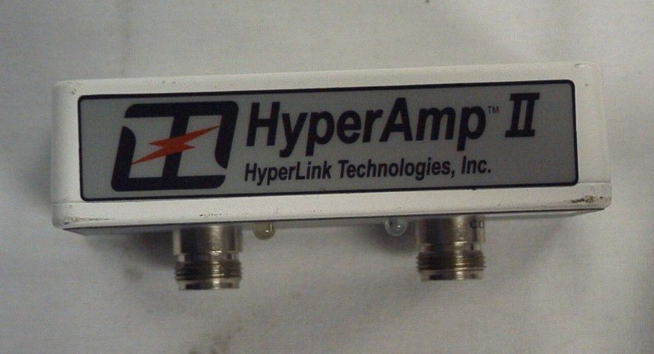
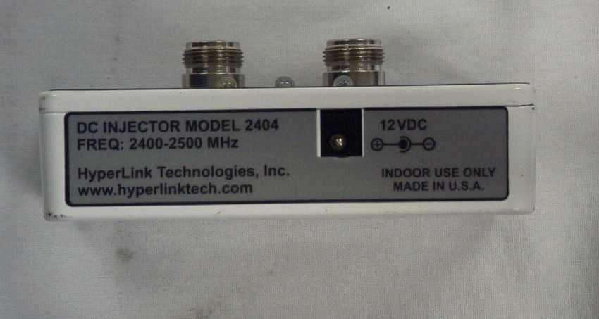
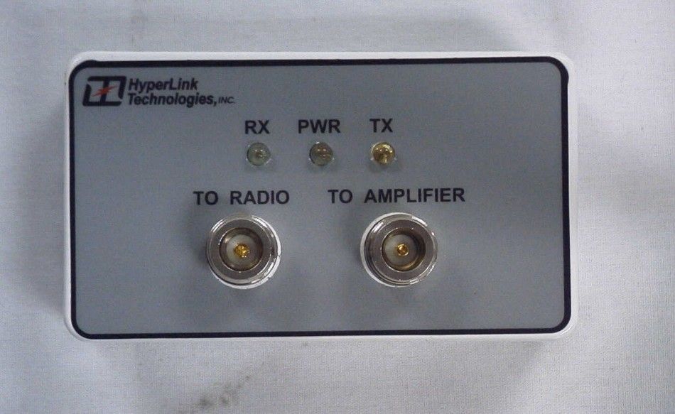
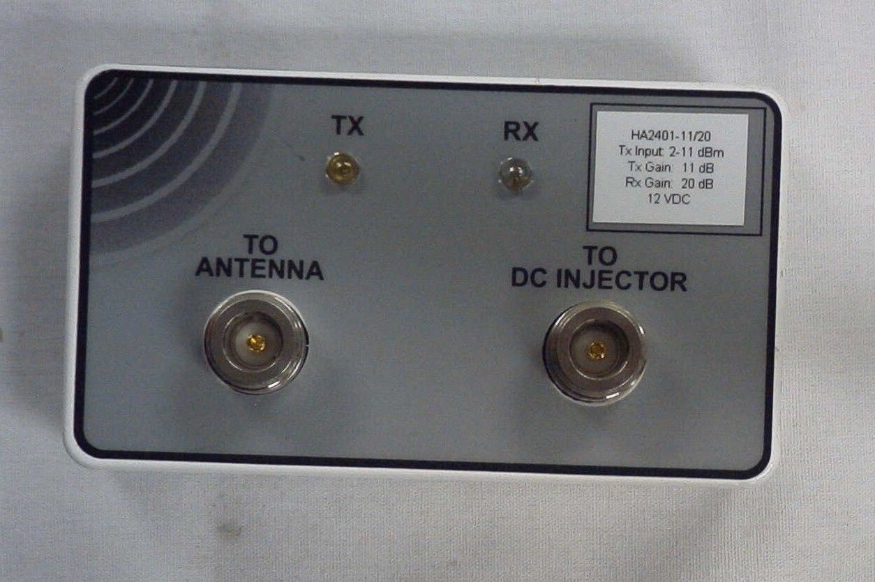
849 NW State Road 45 • P. O. Box 370 • Newberr y, Florida 32669 USA Telephone (352) 472-5500 • (888) 472-2424 • FAX (352) 472-2030 • email: [email protected] 8/28/00 Mr. Joe Dichoso Federal Communications Commission Authorization and Evaluation Division 7435 Oakland Mills Road Columbia, MD 21046 REF: Speedcom Wireless International Corp.’s FCC ID: NCBSLXE Confirmation #: EA97480 Your correspondence ID # 15717 Dear Joe: The amplifier I tested with was HyperLink’s model number HA2401-11/20; the 11 being the transmit gain in dB and the 20 being the receive gain in dB. The photos of the amplifier should reflect this information. It is possible that they sent a generic schematic as they make amplifiers in this case style with different gains. I also believe the 1 Watt rating is for a CW or narrowband signal and not a wideband signal. The owners manual stating 38 mW is the generic users manual for Speedcom and should have been updated for this particular product to reflect the 88 mW power (an oversight on the publications person). The 38 mW rating is for a previous model unit without an amplifier. The manual to be included with this model unit will have the 88 mW power listed. All measurements were carried out with this power amplifier operating in the system and at the antenna connector. Best Regards, Mario R. de Aranzeta Engineer
Test Report
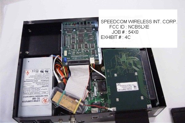
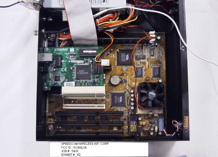
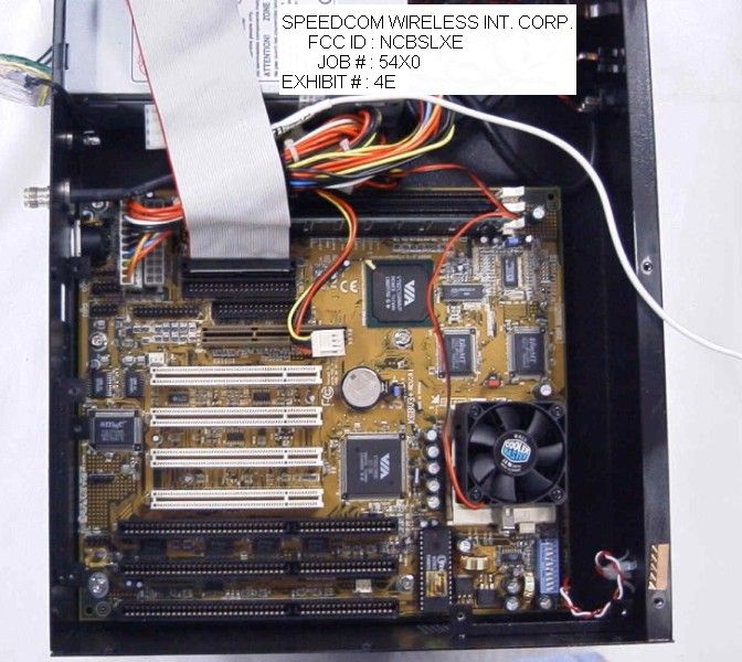
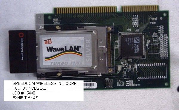
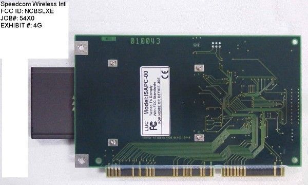
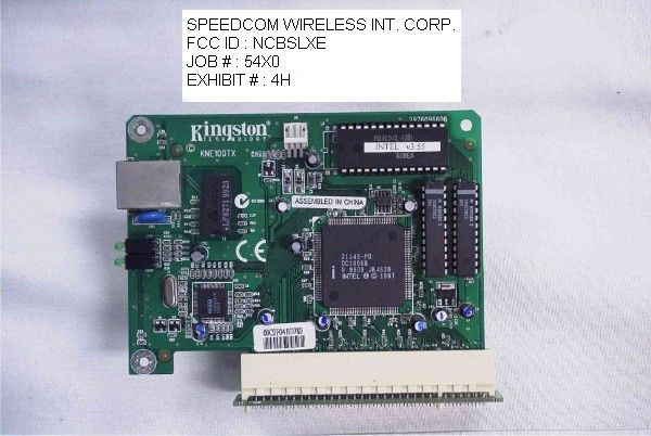
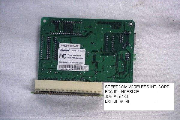
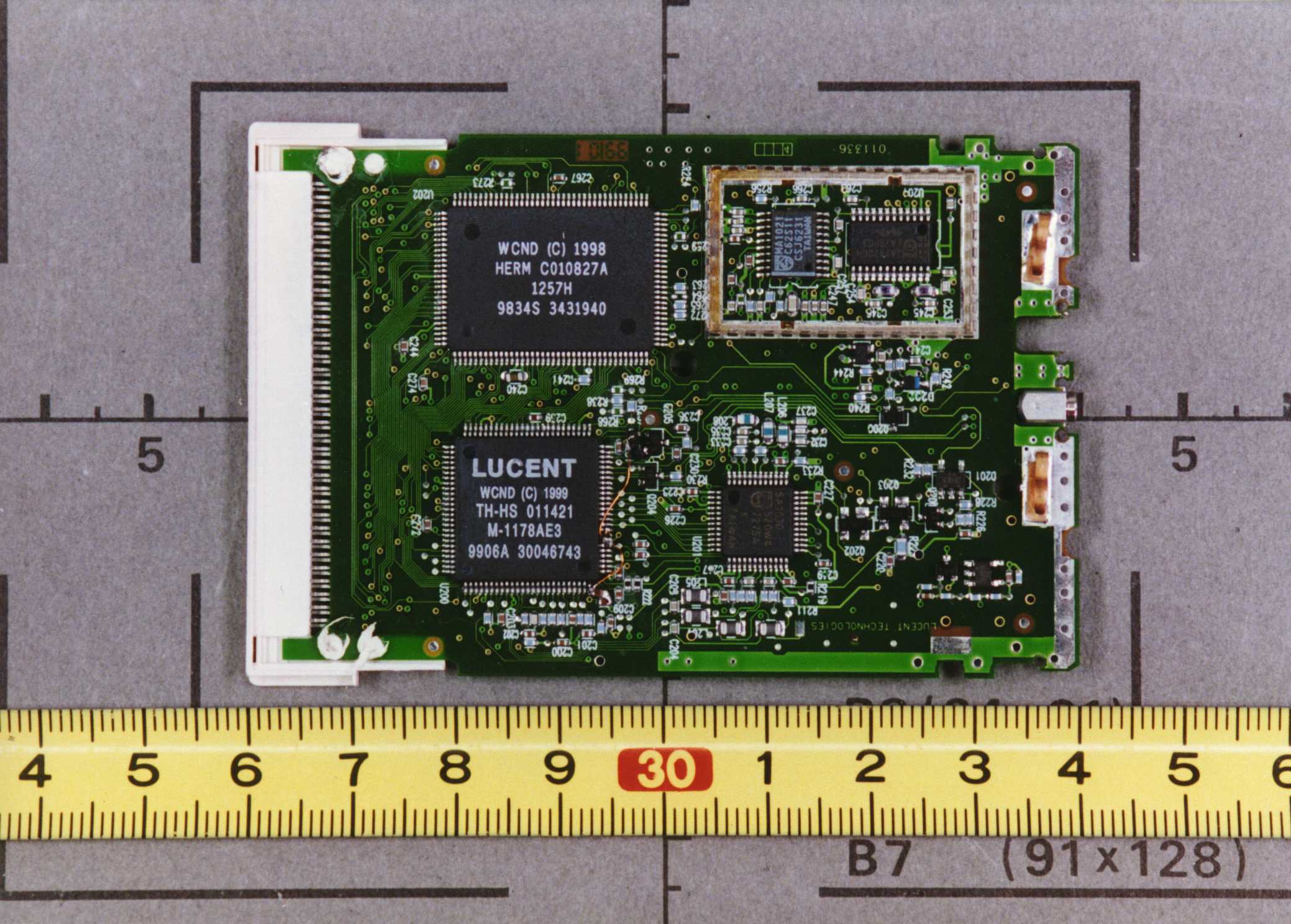
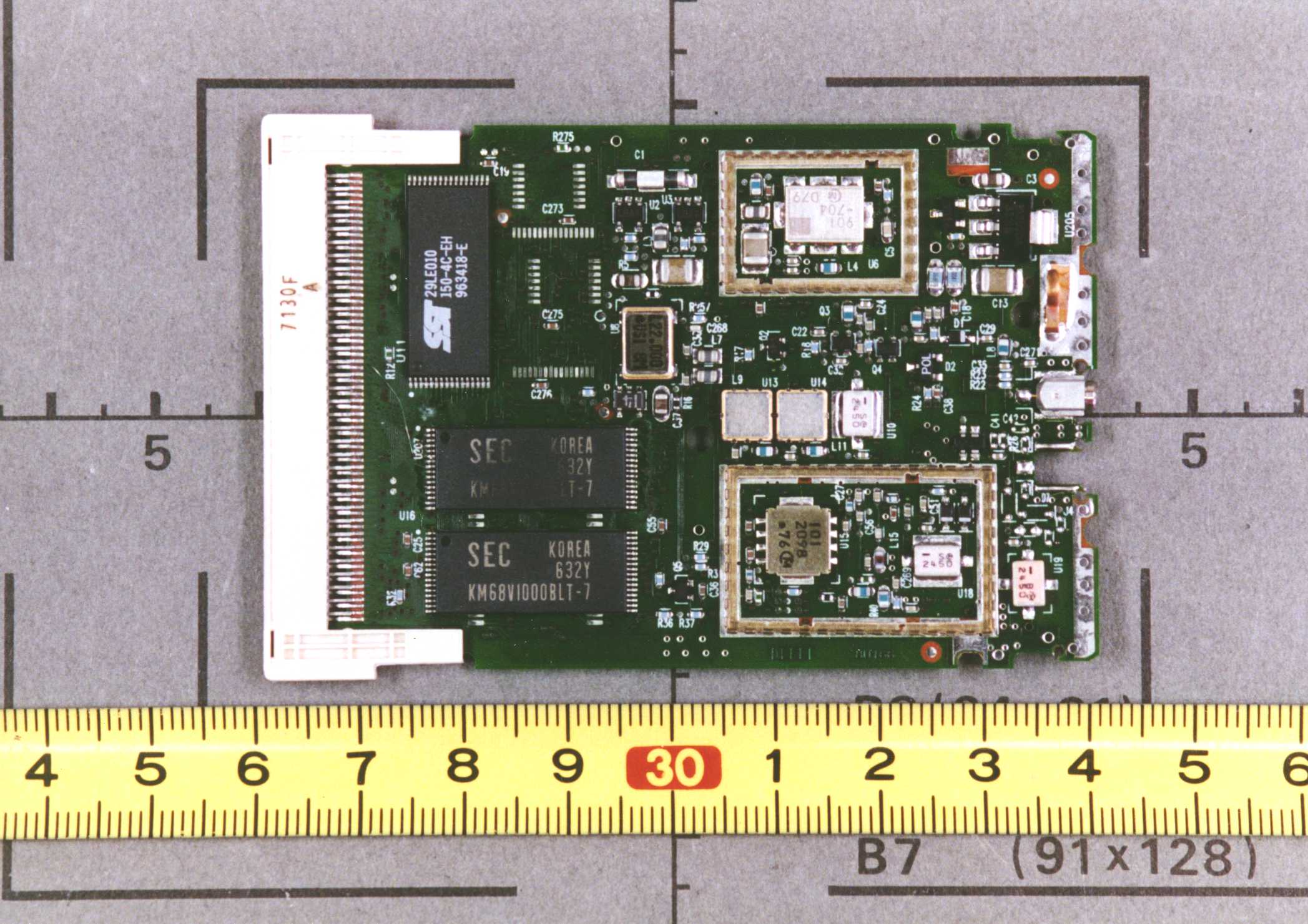
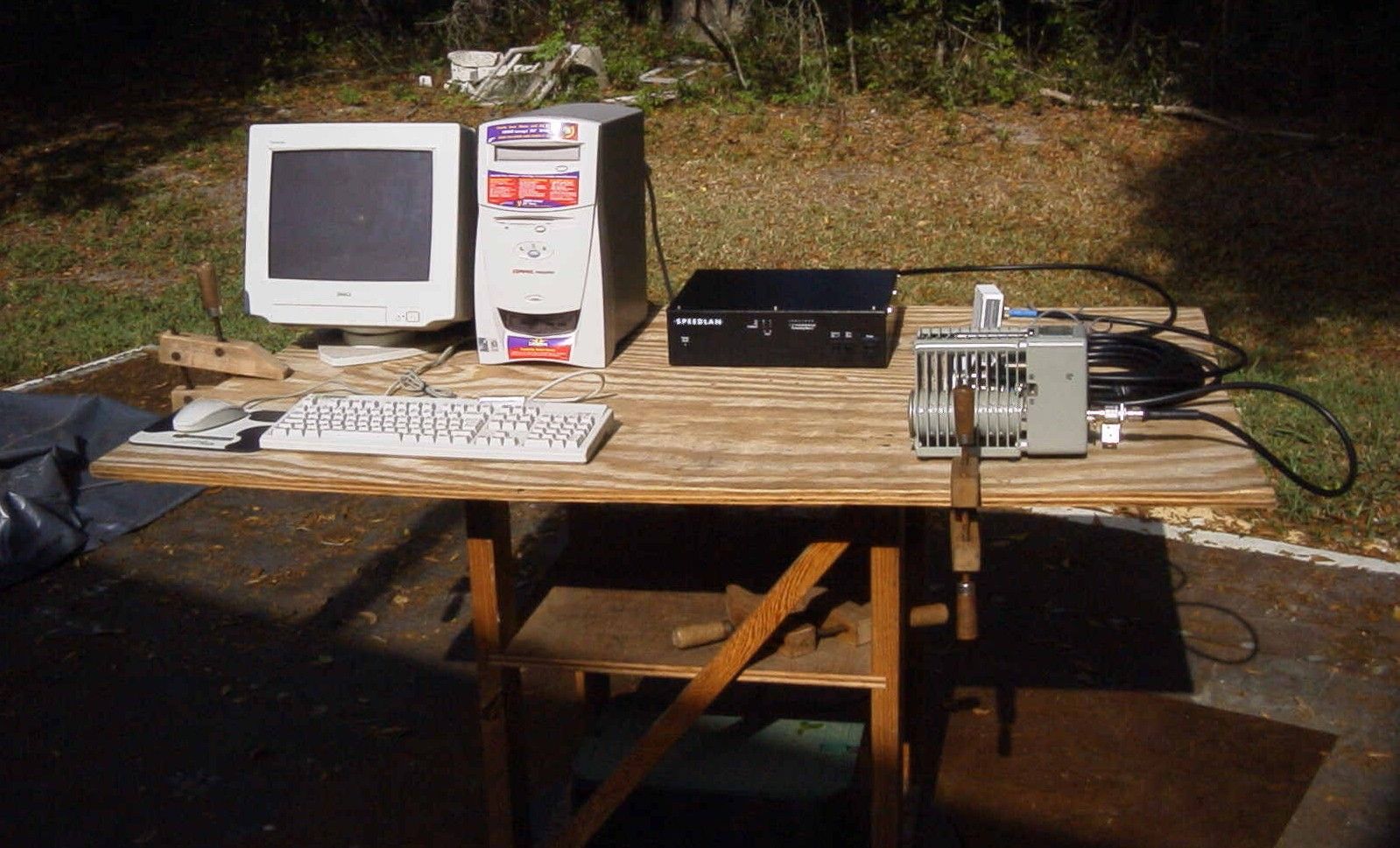
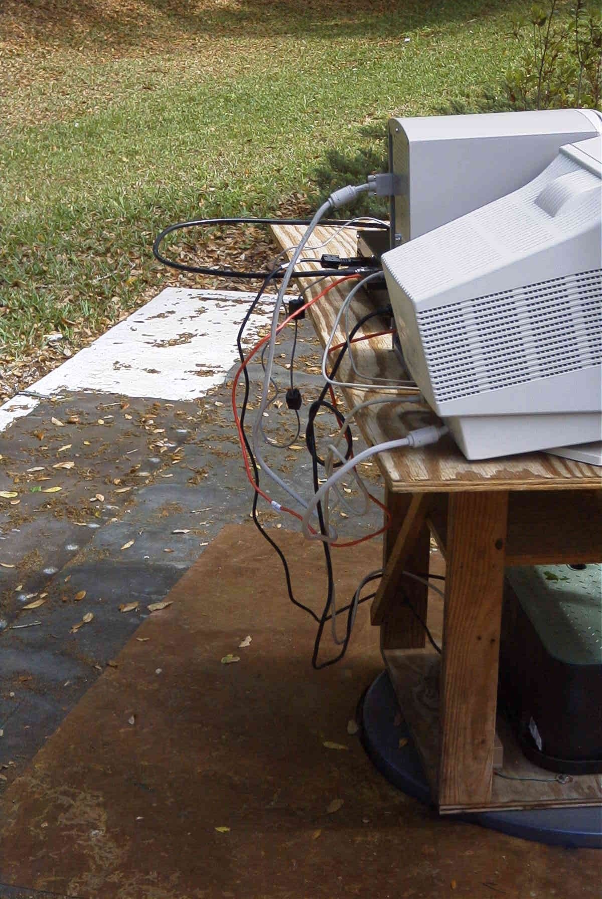
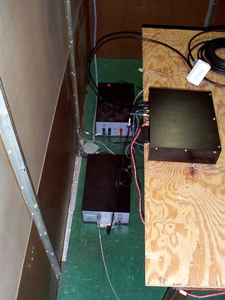
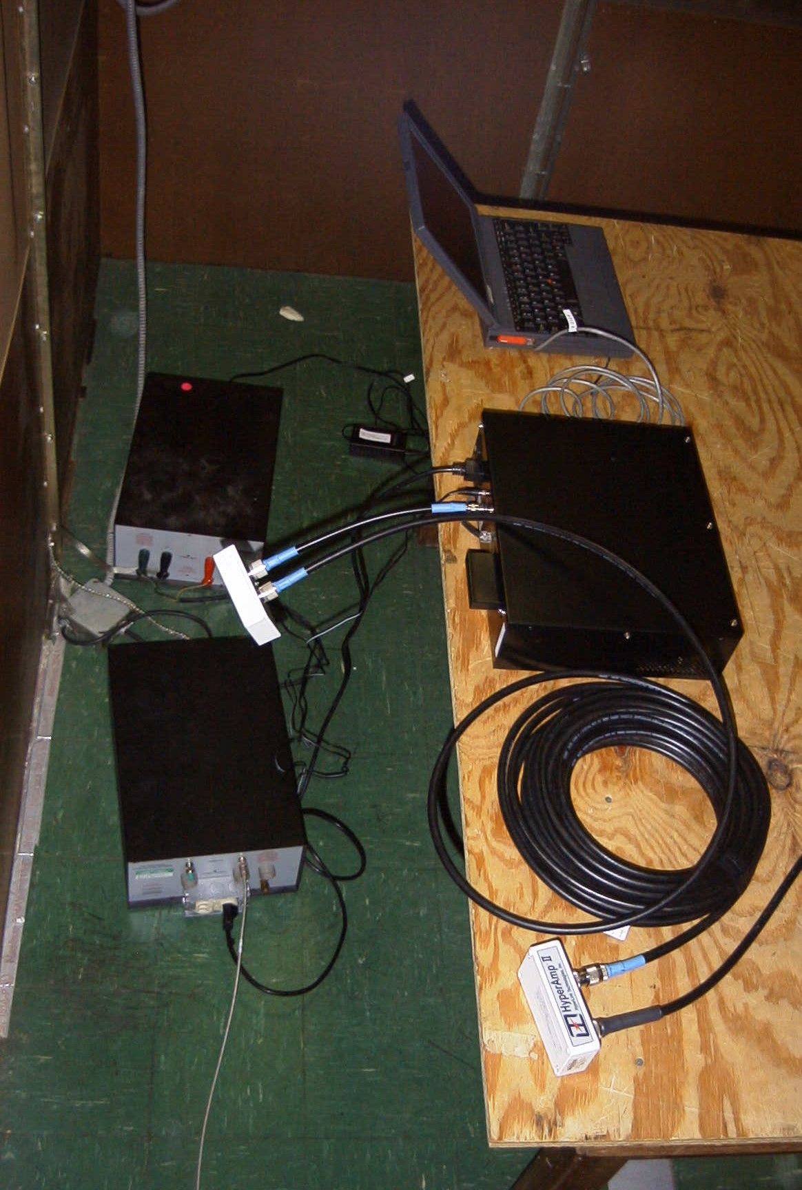
APPLICANT: SPEEDCOM WIRELESS INTERNATIONAL CORP. FCC ID: NCBSLXE TABLE OF CONTENTS TEST REPORT CONTAINING: PAGE 1.............LETTER REQUESTING CONFIDENTIALLY AND EXPLANATION PAGE 2.............TEST EQUIPMENT LIST & TEST PROCEDURE PAGE 3.............PRODUCT DESCRIPTION PAGE 4.............POWER LINE CONDUCTED INTERFERENCE PAGE 5.............BANDWIDTH AND POWER OUTPUT PAGE 6.............METHOD OF MEASURING RF CONDUCTED SPURIOUS EMISSIONS AND SPURIOUS EMISSIONS AT ANTENNA TERMINALS PAGE 7-8...........RADIATION INTERFERENCE TEST DATA AND METHOD OF MEASURING RADIATED EMISSIONS PAGE 9.............POWER SPECTRAL DENSITY PAGE 10.............PROCESSING GAIN EXHIBIT ATTACHMENTS: EXHIBIT 1...........POWER OF ATTORNEY LETTER EXHIBIT 2...........FCC ID LABEL SAMPLE EXHIBIT 3...........SKETCH OF FCC ID LABEL LOCATION EXHIBIT 4A..........FRONT VIEW EXTERNAL PHOTO EXHIBIT 4B..........REAR VIEW EXTERNAL PHOTO EXHIBIT 4C-4D.......CHASSIS VIEW INTERNAL PHOTO EXHIBIT 4E..........INTERNAL SOLDER VIEW PHOTO EXHIBIT 4F..........INTERNAL COMPONENT VIEW - TRANSCEIVER BOARD EXHIBIT 4G..........INTERNAL SOLDER VIEW - TRANSCEIVER BOARD EXHIBIT 4H..........INTERNAL COMPONENT VIEW NETWORK INTERFACE BD EXHIBIT 4I..........INTERNAL SOLDER VIEW NETWORK INTERFACE BD EXHIBIT 5...........BLOCK DIAGRAM EXHIBIT 6...........ASSEMBLY LIST EXHIBIT 7...........INSTRUCTION MANUAL EXHIBIT 8...........6dB BANDWIDTH PLOT EXHIBIT 9...........BAND EDGE PLOT EXHIBIT 10..........SPECTRAL DENSITY PLOT EXHIBIT 11A-11B.....POWER LINE CONDUCTED PLOTS APPLICANT: SPEEDCOM WIRELESS INTERNATIONAL CORP. FCC ID: NCBSLXE REPORT NO.: T:\CUS\S\SPEED\SPE54U0\54X0.RPT TABLE OF CONTENTS LIST 7 APRIL 2000 Federal Communications Commission Authorization and Evaluation Division 7435 Oakland Mills Road Columbia, MD 21046 SUBJECT: SPEEDCOM WIRELESS INTERNATIONAL CORP. FCCID: NCBSLXE To Whom It May Concern: This will serve as a request for confidentiality for the schemat- ics for the radio. The schematics will be sent directly from the manufacturer to the FCC upon request. Once the review of the application is complete and the schematics are no longer needed, they must be returned to the manufacturer, where they were sent from. The attached application is for a direct sequence spread spectrum assembly, made up of the Bridge/Radio, Voltage Injector, 50 foot of coax, an amplifier, 10 foot of coax, a lightening arrestor, and a parabolic antenna. This system is has only one type of antenna, a parabolic dish that has 24dBi. SPEEDCOM WIRELESS INTERNATIONAL CORP. purchases standard antennas from the manufacturers with unique connectors, a reverse TNC, on them. The user manual will have the following statement in it; "WARNING! ALL PERSONNEL SHOULD STAY AT LEAST 1 METER (3.5') FROM ANTENNA TO AVOID EXPOSURE TO POSSIBLE MICROWAVE ENERGY.", FCC rules 15.247(b)(4). The antenna is intended to be use outside. Should you have any questions or require any further information with regards to this, please feel free to contact me. Sincerely, S. S. Sanders SSS/sh Encl. APPLICANT: SPEEDCOM WIRELESS INTERNATIONAL CORP. FCCID: NCBSLXE REPORT #: T:\CUS\S\SPEED\SPE54U0\54X0.RPT PAGE #: 1 TEST EQUIPMENT LIST 1._X_Spectrum Analyzer: HP 8566B-Opt 462, S/N 3138A07786, w/ preselector HP 85685A, S/N 3221A01400, Quasi-Peak Adapter HP 8565OA, S/N 3303A01690 & Preamplifier HP 8449B-OPT H02, S/N 3008A00372 Cal. 10/17/99 2._X_Biconnical Antenna: Eaton Model 94455-1, S/N 1057 3._X_Log-Periodic Antenna: Electro-Metrics Model EM-6950, S/N 632 4._X_Double-Ridged Horn Antenna: Electro-Metrics Model RGA-180, 1-18 GHz, S/N 2319 Cal. 4/27/99 5.___Horn 40-60GHz: ATM Part #19-443-6R 6._X_Line Impedance Stabilization Network: Electro-Metrics Model ANS-25/2, S/N 2604 Cal. 2/9/00 7.___Temperature Chamber: Tenney Engineering Model TTRC, S/N 11717-7 8._X_Peak Power Meter: HP Model 8900C, S/N 2131A00545 Cal 7/19/99 9._X_Opean Area Test Site #1-3meters Cal. 12/22/99 TEST PROCEDURE GENERAL: This report shall NOT be reproduced except in full without the written approval of TIMCO ENGINEERING, INC. Shielded interface cables were used in all cases except for cables connecting to the telephone line and the power cords. A test program was run which simulated a normal data transmission on a network. POWER LINE CONDUCTED INTERFERENCE: The procedure used was ANSI STAN- DARD C63.4-1992 using a 50uH LISN. Both lines were observed with the UUT transmitting. The bandwidth of the spectrum analyzer was 10kHz with an appropriate sweep speed. The ambient temperature of the UUT was 76oF with a humidity of 55%. BANDWIDTH 6.0dB: The measurements were made with the spectrum analyz- er's resolution bandwidth(RBW)=1.0MHz and the video bandwidth(VBW) =3.0MHz and the span set as shown on plot. POWER OUTPUT: The RF power output was measured at the antenna feed point using a peak power meter. ANTENNA CONDUCTED EMISSIONS: The RBW=100KHz, VBW=300KHz and the span set to 10.0MHz and the spectrum was scanned from 30MHz to the 10th Harmonic of the fundamental. Above 1.0GHz the resolution bandwidth was 1.0MHz and the VBW = 3.0MHz and the span to 50MHz. RADIATION INTERFERENCE: The test procedure used was ANSI STANDARD C63.4-1992 using a HEWLETT PACKARD spectrum analyzer with a prese- lector. The bandwidth(RBW) of the spectrum analyzer was 100kHz up to 1GHz and 1.0MHz above 1GHz with an appropriate sweep speed. The VBW above 1.0GHz was = 3.0MHz. The analyzer was calibrated in dB above a microvolt at the output of the antenna. The ambient temperature of the UUT was 71oF with a humidity of 56%. APPLICANT: SPEEDCOM WIRELESS INTERNATIONAL CORP. FCCID: NCBSLXE REPORT #: T:\CUS\S\SPEED\SPE54U0\54X0.RPT PAGE #: 2 PRODUCT DESCRIPTION: The NCBSLXE is a direct sequence spread spectrum radio that operates in the 2421MHz band. / - - -- - - - - - - - - - - - - \ /----------\ /------------\ /---------\ | | 10" | | | | | LAPTOP | | CABLE |-| NETWORK |---| CPU | | |ASSEMBLY | | BRIDGE | | | | \----------/ | WITH | \---------/ | /----------\ | RADIO | | | Voltage…
Text truncated - open the document above for the full version.
Test Report
Measurement file output name is: 5mbit.cnd Input command file name is: INPUT.CMD Note: 5.5 Mbit, 6 dB SIR tested for ( 15 dB SNR - 10.4 + 1 impl. losses). Input CW correction level: 6 dB Takes into account 1 dB of implementation loss (allowed 2 dB). Lowcount is: 1000 messages Only RxD errors are taken into account since these need better SIR then preamble at 1 MBit Highcount is: 50000 messages Attention: Input the red cells for correct spreadsheet calculations! total errors 45 out of 280 measurement points. Rx level DUT is: -53 dBm percentage 16.07% Number of received data errors as a function of frequency and interference level OK? =<20%, OK Not measured combinations listed as "-1" HIJKLMN O PQ RS Uncorrected Interference level dialed at CW generator -60 -59 -58 -57 -56 -55 -54 -53 -52 RxD Errors PDA RxD Errors PDA Both error True CW interference level at receiver input (dBm) detected missing detected missing RxD and -66 -65 -64 -63 -62 -61 -60 -59 -58 full test full test up to CW AT CW PDA J/S ratio (dB) -13 #PDA -12 #PDA -11 #PDA -10 #PDA -9 #PDA -8 #PDA -7 #PDA -6 #PDA -5 #PDA range range =< -59 dBm = -59 dBm =< -59 dBm Frequency (Hz) (J/S = -5-1 dB) (J/S = -5-1 dB) time date 2409000000 0 1000 0 1000 0 1000 0 1000 0 1000 0 1000 0 1000 0 1000 0 50000 OK, 0 RxD error s OK, No PDA err o 000 15:53:49 4/15/99 2409050000 0 1000 0 1000 0 1000 0 1000 0 1000 0 1000 0 1000 0 1000 0 50000 OK, 0 RxD error s OK, No PDA err o 000 15:52:18 4/15/99 2409100000 0 1000 0 1000 0 1000 0 1000 0 1000 0 1000 0 1000 0 1000 0 50000 OK, 0 RxD error s OK, No PDA err o 000 15:50:48 4/15/99 2409150000 0 1000 0 1000 0 1000 0 1000 0 1000 0 1000 0 1000 0 1000 0 50000 OK, 0 RxD error s OK, No PDA err o 000 15:49:19 4/15/99 2409200000 0 1000 0 1000 0 1000 0 1000 0 1000 0 1000 0 1000 0 1000 0 50000 OK, 0 RxD error s OK, No PDA err o 000 15:47:48 4/15/99 2409250000 0 1000 0 1000 0 1000 0 1000 0 1000 0 1000 0 1000 0 1000 0 50000 OK, 0 RxD error s OK, No PDA err o 000 15:46:19 4/15/99 2409300000 0 1000 0 1000 0 1000 0 1000 0 1000 0 1000 0 1000 0 1000 0 50000 OK, 0 RxD error s OK, No PDA err o 000 15:44:49 4/15/99 2409350000 0 1000 0 1000 0 1000 0 1000 0 1000 0 1000 0 1000 0 1000 0 50000 OK, 0 RxD error s OK, No PDA err o 000 15:43:18 4/15/99 2409400000 0 1000 0 1000 0 1000 0 1000 0 1000 0 1000 0 1000 0 1000 0 50000 OK, 0 RxD error s OK, No PDA err o 000 15:41:49 4/15/99 2409450000 0 1000 0 1000 0 1000 0 1000 0 1000 0 1000 0 1000 0 1000 0 50000 OK, 0 RxD error s OK, No PDA err o 000 15:40:18 4/15/99 2409500000 0 1000 0 1000 0 1000 0 1000 0 1000 0 1000 0 1000 0 1000 0 50000 OK, 0 RxD error s OK, No PDA err o 000 15:38:48 4/15/99 2409550000 0 1000 0 1000 0 1000 0 1000 0 1000 0 1000 0 1000 0 1000 0 50000 OK, 0 RxD error s OK, No PDA err o 000 15:37:18 4/15/99 2409600000 0 1000 0 1000 0 1000 0 1000 0 1000 0 1000 0 1000 0 1000 0 50000 OK, 0 RxD error s OK, No PDA err o 000 15:35:48 4/15/99 2409650000 0 1000 0 1000 0 1000 0 1000 0 1000 0 1000 0 1000 0 1000 0 50000 OK, 0 RxD error s OK, No PDA err o 000 15:34:18 4/15/99 2409700000 0 1000 0 1000 0 1000 0 1000 0 1000 0 1000 0 1000 0 1000 0 50000 OK, 0 RxD error s OK, No PDA err o 000 15:32:48 4/15/99 2409750000 0 1000 0 1000 0 1000 0 1000 0 1000 0 1000 0 1000 0 1000 0 50000 OK, 0 RxD error s OK, No PDA err o 000 15:31:17 4/15/99 2409800000 0 1000 0 1000 0 1000 0 1000 0 1000 0 1000 0 1000 0 1000 0 50000 OK, 0 RxD error s OK, No PDA err o 000 15:29:47 4/15/99 2409850000 0 1000 0 1000 0 1000 0 1000 0 1000 0 1000 0 1000 0 1000 0 50000 OK, 0 RxD error s OK, No PDA err o 000 15:28:17 4/15/99 2409900000 0 1000 0 1000 0 1000 0 1000 0 1000 0 1000 0 1000 0 1000 0 50000 OK, 0 RxD error s OK, No PDA err o 000 15:26:46 4/15/99 2409950000 0 1000 0 1000 0 1000 0 1000 0 1000 0 1000 0 1000 0 1000 0 50000 OK, 0 RxD error s OK, No PDA err o 000 15:25:16 4/15/99 2410000000 0 1000 0 1000 0 1000 0 1000 0 1000 0 1000 0 1000 0 1000 0 50000 OK, 0 RxD error s OK, No PDA err o 000 15:23:45 4/15/99 2410050000 0 1000 0 1000 0 1000 0 1000 0 1000 0 1000 0 1000 0 1000 0 50000 OK, 0 RxD error s OK, No PDA err o 000 15:22:15 4/15/99 2410100000 0 1000 0 1000 0 1000 0 1000 0 1000 0 1000 0 1000 0 1000 0 50000 OK, 0 RxD error s OK, No PDA err o 000 15:20:45 4/15/99 2410150000 0 1000 0 1000 0 1000 0 1000 0 1000 0 1000 0 1000 0 1000 0 50000 OK, 0 RxD error s OK, No PDA err o 000 15:19:14 4/15/99 2410200000 0 1000 0 1000 0 1000 0 1000 0 1000 0 1000 0 1000 0 1000 0 50000 OK, 0 RxD error s OK, No PDA err o 000 15:17:44 4/15/99 2410250000 0 1000 0 1000 0 1000 0 1000 0 1000 0 1000 0 1000 0 1000 0 50000 OK, 0 RxD error s OK, No PDA err o 000 15:16:14 4/15/99 2410300000 0 1000 0 1000 0 1000 0 1000 0 1000 0 1000 0 1000 0 1000 0 50000 OK, 0 RxD error s OK, No PDA err o 000 15:14:43 4/15/99 2410350000 0 1000 0 1000 0 1000 0 1000 0 1000 0 1000 0 1000 0 1000 0 50000 OK, 0 RxD error s OK, No PDA err o 000 15:13:13 4/15/99 2410400000 0 1000 0 1000 0 1000 0 1000 0 1000 0 1000 0 1000 0 1000 0 50000 OK, 0 RxD error s OK, No PDA err o 000 15:11:42 4/15/99 2410450000 0 1000 0 1000 0 1000 0 1000 0 1000 0 1000 0 1000 0 1000 0 50000 OK, 0 RxD error s OK, No PDA err o 000 15:10:12 4/15/99 2410500000 0 1000 0 1000 0 1000 0 1000 0 1000 0 1000 0 1000 0 1000 0 50000 OK, 0 RxD error s OK, No PDA err o 000 15:08:42 4/15/99 2410550000 0 1000 0 1000 0 1000 0 1000 0 1000 0 1000 0 1000 0 1000 0 50000 OK, 0 RxD error s OK, No PDA err o 000 15:07:12 4/15/99 2410600000 0 1000 0 1000 0 1000 0 1000 0 1000 0 1000 0 1000 0 1000 0 50000 OK, 0 RxD error s OK, No PDA err o 000 15:05:42 4/15/99 2410650000 0 1000 0 1000 0 1000 0 1000 0 1000 0 1000 0 1000 0 1000 0 50000 OK, 0 RxD error s OK, No PDA err o 000 15:04:12 4/15/99 2410700000 0 1000 0 1000 0 1000 0 1000 0 1000 0 1000 0 1000 0 1000 0 50000 OK, 0 RxD error s OK, No PDA err o 000 15:02:42 4/15/99 2410750000 0 1000 0 1000 0 1000 0 1000 0 1000 0 1000 0 1000 0 1000 0 50000 OK, 0 RxD error s OK, No PDA err o 000 15:01:11 4/15/99 2410800000 0 1000 0 1000 0 1000 0 1000 0 1000 0 1000 0 1000 0 1000 0 50000 OK, 0 RxD …
Text truncated - open the document above for the full version.
Test Report
Nederland B.V. WCND FCC ID: WLPC24H/WLPCE24H Report No. 011734, Rev. B TEST REPORT Subject: Processing Gain For WaveLAN IEEE PC CARD type 2 HS Ref.: FCC Rules 47 CFR Part 15, Section 5.247d Report Prepared by: Maarten Visee May 6, 1999 Name Signature Date Concurrence: 1. Director of Engineering Bruce Tuch May 6, 1999 Name Signature Date 2. Team Captain Frans Hoekstra May 6, 1999 Name Signature Date FCC Processing Gain Measurements Results, FCCID WLPC24H/WLPCE24H, Report No. 011734, Rev. B. Lucent WCND Confidential ©1999 Lucent WCND Confidential Information ©1999 FCC Processing Gain Measurements Results, FCCID WLPC24H/WLPCE24H, Report No. 011734, Rev. B. Lucent WCND Confidential ©1999 Date Section Description 04/16/99, Rev. A Initial release. 05/6/99, Rev. B 2 Changed spreading gain into processing gain. 4.1 For data rates of 5.5 and 11 Mbit/s changed processing gain requirements of 9 dB into 10 dB. 4.2 Changed description for demodulated data availability at the interconnection between RF and DSP into the interconnection between DSP and digital circuits. Changed spreading gain into processing gain. 7.2, 7.3 Changed sub sections Measurement Results and Measurement Conclusion. Annex A Updated flow chart. Change History: FCC Processing Gain Measurements Results, FCCID WLPC24H/WLPCE24H, Report No. 011734, Rev. B. Lucent WCND Confidential ©1999 This document describes the Receiver Processing Gain verification measurements performed at the WaveLAN-II PC-Card Type 2, according to Ref.[2]. The Lucent WaveLAN-II PC-Card Type 2 product confirms to the minimum required 10 dB processing gain, as set forth by the FCC for operation in the 2.4 GHz ISM band. 1- Document FCC 97-114, Appendix C, Guidance on Measurements for Direct Sequence Spread Spectrum Systems. 2- Hardware Functional Specification for WaveLAN-II Embedded, High Speed, Doc. No. 011735, Rev. A, Source Organization Lucent Technologies WCND Utrecht. 3- Viterbi, A. J., Principles of Coherent Communications, New York, McGraw-Hill 1966. 4- Proakis, J.G., Digital Communications, New York, McGraw-Hill 1989, page 270. 4.1 Test introduction - FCC requirements: Part of FCC certification for the Lucent WaveLAN IEEE 802.11 High Speed compliant Network Interface Card (NIC) is a processing gain test. This test proves that the receiver of the tested product employs a true spread spectrum device receiver structure, taking full advantage of the direct sequence spread spectrum modulation technique. This test verifies the receiver processing gain to be 10 dB or more for a data rate of 1, 2, 5.5 and 11 Mbit/s, by monitoring the Bit Error Rate (BER) of the product under test for each data rate, while operating under strict defined received signal conditions. Several methods of showing compliance to the rules are possible, from a stepped CW jammer to a continuous sweeping CW interferer. For this test the discrete stepped CW jammer method was chosen, as described in Ref.[1]. 1.Summary: 2.Conclusion: 3.References: 4.Measurement description: FCC Processing Gain Measurements Results, FCCID WLPC24H/WLPCE24H, Report No. 011734, Rev. B. Lucent WCND Confidential ©1999 Therefore a receiver input signal is applied to the product under test, in the presence of a Continuous Wave (CW) interference source, also referred to as CW jammer. The test takes place at the product Functional Specification (Ref.[2]) specified conditions for BER rate measurements, specifying a BER equal or better than 10^-8 at a receiver input level of -55 dBm. For practical reasons these test are performed at -55 dBm or -53 dBm. This small deviation from the Functional Specification should not cause any deviation from the specified Bit Error Rate, since the received levels are well above the thermal noise. The test criteria for meeting the minimal processing gain is such that it takes the theoretical calculated SNR for the applied modulation technique and specified BER as a reference. From this given SNR the processing gain is subtracted, yielding the CW Jammer to Signal ratio J/S. From Ref. [4], likewise as Ref.[3] consulted in Ref. [1], it is determined that for a BER of 10^-8 the SNR (S/N)o equals: 13 dB @ 1 Mbit/s, 15 dB @ 2 Mbit/s, 15 dB @ 5.5 Mbit/s, 18 dB @ 11 Mbit/s. Thus the J/S ratio for a processing gain of 10 dB that must be met is calculated as: -13 + 10 = -3 dB @ 1 Mbit/s (DBPSK), -15 + 10 = -5 dB @ 2 Mbit/s (DQPSK), -15 + 10 = -5 dB @ 5.5 Mbit/s (CCK), -18 + 10 = -8 dB @ 11 Mbit/s (CCK). Two types of measurement corrections are allowed for as described in Ref.[1]. The first taking into account 2 dB implementation losses, thus increasing the absolute J/S ratio by 2 dB. The second correction allows for deleting the 20% worst- case frequencies in the processing gain test that causes the test at that CW interference to fail. This implies that for the considered 14 MHz wide measurement interval the worst case 57 CW jammer frequencies can be ignored, being those that result in FCC Processing Gain Measurements Results, FCCID WLPC24H/WLPCE24H, Report No. 011734, Rev. B. Lucent WCND Confidential ©1999 received data errors/missing frames (20% of 14 MHz *(1 MHz/50 KHz) + 1 = (20% * 281) + 1 = 57). FCC Processing Gain Measurements Results, FCCID WLPC24H/WLPCE24H, Report No. 011734, Rev. B. Lucent WCND Confidential ©1999 4.2 Test sequence: The measurements are performed at a 50 KHz CW jammer raster. For each CW jammer frequency 10^8 bits are transmitted by the reference transmitter, and received by the product under test. For practical reasons 50.000 messages are transmitted. After blanking out frame overhead 1927 bits per frame are monitored. This results in 50.000 * 1927 = 9650000 transmitted bits for a BER test, which is a mere 1.4% less than the targeted 10^8 bits. Though it would be more elegant to show BER compliance for at least say ten times 10^8 transmitted/received bits, the time involved with this grows significantly. Since the CW interferer is stepped in a 50 KHz raster, covering the re…
Text truncated - open the document above for the full version.
Contact Information
Applicant
John Dyndul(Product Certification Manager)
Technical Contact
HyperlinkPeter Roth
561-995-2256
1201 Clint Moore Road · Boca Raton, Florida · United States
Non-Technical Contact
Timco Engineering, Inc.Eric F Dobson
[email protected]888-472-2424
Test Firm
Timco Engineering, Inc.S Sanders
Technical Specifications
| # | Rule Parts | Frequency Range | Power Output |
|---|---|---|---|
| 1 | 15C | 2.42 GHz - 2.42 GHz | 88.00 mW |
Other Applications from Wave Wireless Networking
NCBSL9101A
Dec 11, 2003Spread Spectrum Transmitter
Equipment Class
DTS - Digital Transmission System
NCBSL9102A
Dec 09, 2003SPREAD SPECTRUM TRANSMITTER
Equipment Class
DTS - Digital Transmission System
NCBSL9102
May 08, 2002Spread Spectrum Transmitter
Equipment Class
DTS - Digital Transmission System
NCBSL9101
May 06, 2002Spread Spectrum Transmitter
Equipment Class
DTS - Digital Transmission System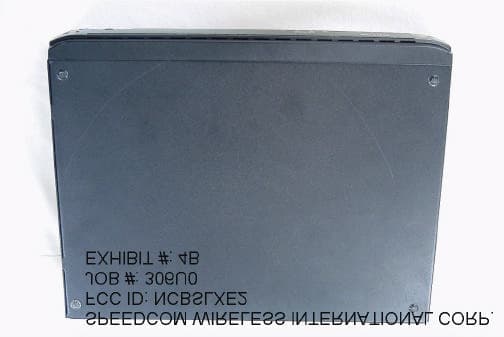
NCBSLXE2
Apr 11, 2002Spread Spectrum Transmitter
Equipment Class
DSS - Part 15 Spread Spectrum Transmitter