NTTSX1124Part 21 MMDS/MDS transceiver
WJ Communications, Inc.
Click to zoom
Application Details
- Equipment Class
- TNB - Licensed Non-Broadcast Station Transmitter
- Date of Grant
- Sep 06, 2000
- Application Purpose
- Original Equipment
- Date of Application
- Jul 31, 2000
- Equipment Note
- Part 21 MMDS/MDS transceiver
- Frequency Range
- 2150.00000000 - 2162.00000000
- Company
- WJ Communications, Inc.
- Country
- United States
Documents & Files
Document Text
Text extracted from the exhibit documents filed with the FCC. Open a document above to read the original.
ID Label/Location Info
FCC ID Label and Label Location for Watkins-Johnson FCC ID: NTTSX1124 Watkins-Johnson SX1124 FCC ID: NTTSX1124 This device complies with Part 15 of the FCC Rules. Operation is subject to the following two conditions: (1) This device may not cause harmful interference, and (2) This device must accept any interference received, including interference than may cause undesired operation
Test Report
Watkins Johnson.FCC ID: NTTSX1124 page 1 of 31 EXHIBITS EXHIBIT 1:Letter Requesting Confidentiality under Sec. 0.457(d) EXHIBIT 2: Product Description and Operation Overview EXHIBIT 3:Information for which Confidentiality is Requested Schematics Block Diagrams Theory of Operation EXHIBIT 4:Product Photographs EXHIBIT 5:Bill of Materials (BOM) EXHIBIT 6:User Manual and FCC ID Label EXHIBIT 7:RF Hazard Information per Sec. 1.1307 EXHIBIT 8: Report of Measurements EXHIBIT 9: Data Graphs – Emissions Masks EXHIBIT 10: Data Graphs - Out of Band Emissions EXHIBIT 11: IF Card TX Signals to RF Module Watkins Johnson.FCC ID: NTTSX1124 page 2 of 31 EXHIBIT 1:Letter Requesting Confidentiality under Sec. 0.457(d) Watkins Johnson.FCC ID: NTTSX1124 page 3 of 31 Thomas N. Cokenias EMC &Radio Approvals Test & Consulting Services for Commercial, Military, International Compliance P.O. Box 1086 El Granada, CA 94018 20 July 2000 FCC Laboratory 7435 Oakland Mills Road Columbia, MD 21046 Attention: Application Examiner Reviewing Engineer Re: Request for confidentiality per Section 0.459 of FCC Rules Applicant: Watkins Johnson. FCC ID: NTTSX1124 To whom it may concern, Request is hereby submitted, on behalf of my client Watkins Johnson., to withhold from public review certain portions of the application for equipment certification for the referenced FCC identifier. In particular, the following sections of the application and report are requested to be kept confidential: Schematics Block diagrams Theory of operation (P2P Architecture) Rationale for request for confidentiality: Watkins Johnson has invested considerable time and materials in research and development to produce the referenced product. Disclosure of the confidential portions of this application to competitors would give them competitive advantage in developing similar products. The $135 fee for confidentiality has been submitted along with the fee for certification. If you have questions or need further information, please contact the undersigned. Sincerely, THOMAS N. COKENIAS EMC Consultant/Agent for Watkins Johnson. Watkins Johnson.FCC ID: NTTSX1124 page 4 of 31 Tel 650 726 1263 fax 650 726 [email protected] Watkins Johnson.FCC ID: NTTSX1124 page 5 of 31 EXHIBIT 2:Product Description and Operation Overview Watkins Johnson.FCC ID: NTTSX1124 page 6 of 31 The Watkins Johnson FCC ID: NTTSX1124 is a MMDS transceiver operating under the provisions of Part 21 of the Rules. The product functions as a point to point (P2P) wireless router. Refer to the system module diagram below: Product development strategy is to follow a modular approach. Digital data I/O for the initial version of the system will be a line card that will fit into a standard Cisco uBR7246 or 7223 router chassis. For test purposes, a Tektronix arbitrary waveform generator will simulate the signal output of the router/line card combination. The IDU IF card up-link performs the modulation functions of the system. A 330 MHz signal is modulated with the digital data stream using Orthogonal Frequency Division Multiplexing (OFDM) techniques. The system is capable of producing channel bandwidths in 6 MHz multiples. The system will be configurable for use with 1.5, 3.0, and 6.0 MHz channel bandwidths. Digital data I/O AB IDU IF Card SPI IF Card RS 232 Cable PC Controlle r -48volts ODU RF Head RS 232 Cable Bias “T” Watkins Johnson.FCC ID: NTTSX1124 page 7 of 31 For the down-link signal, the IF card demodulates the receiver IF signal from the RF head and routes the demodulated digital information to the digital I/O card. It is anticipated that the IF card will be used with a number of different RF heads, but will provide the same kind of OFDM modulation, the same IF signals, and at the same channel spacing as will be provided for the present application. The IF output RF spectrum is in Exhibit 11. The bias “T” provides DC and the 330 MHz IF signal on a single coaxial cable for routing to the RF head. The ODU RF head produces the RF transmit link at 2150 – 2162 MHz , and houses the receiver LNAs, receiver local oscillator, and the 139 MHz receiver IF bandpass filters and IF amplifiers. The RF head also houses the TX-RF diplexer. The PC controller and RS 232 cables are for system control and set-up for testing purposes. The antenna shown in the diagram is specified but not supplied by Watkins Johnson. The –48 VDC supply shown in the diagram is telephone central office (CO) power or a customer provided supply. SPECIFICATIONS ODU RF Head Frequency range: 2150 - 2162 MHz Power output:30 - 36 dBm maximum, depending on channel bandwidth Channel Bandwidth:1.5 MHz, 3.0 MHz, and 6 MHz configurable IDU IF Head Frequency range:330 MHz 24 MHz clock Power output:330 MHz: -13 dBm nominal (programmable) 24 MHz: -12 dBm nominal Data transfer rate, air link:22 Mbs/sec (6 MHz channel) A detailed description of the theory of operation and product configuration is found in the attached document, rfhea~1.doc.. Watkins Johnson. FCC ID: NTTSX1124 page 8 of 31 System Interconnection uBR 7246/7223 ROUTER POWER FEED PANEL (UBR-WPFD) 1 per line card IF Cable ControlCable 48V DC Power Supply ControlCable Ligh t n in g P r o t ect o r for Control Cable 10 MHz Clock Wireless Modem Line Card (UBN- MCW- PDA) Up to 4 depending upon router Bulkhead Outdoor Unit (UBR- ODU- PAA) Duplexor (UBR- ODD- XXA) IFCable RF Cable ** Provided by Cisco Alignment port Optional cable kit one required for each line card to Power Feed Panel connection Through bulkhead connector ** Mounting Bracket Kit ** Mounting Bracket Kit Betw een-Series Adapter Monitor Cable ** Pluggable Terminal Block Rec eptac le RJ45 (M) RJ45 (M) SMA (M) SMA (M) RJ45 (F) RJ45 (F) SMA (F) SMA (F) SMA(F) SMA(F) SMA(M)SMA(M) BN C( F ) BN C( M) BN C( M) BN C( F ) DB9(M) DB9(F) N(F) N(M) N(M) N (F) N(M) N(M) N(F) ** Lemo(M) Lemo(F) N(F) N(M) xx Ω Spectrum Analyzer N(M) N(F) BN C( F ) 3.5 mm Mono Phone Jack 3.5 mm Mono Phone Plug ** Ground Lug Pigtail between unitand top …
Text truncated - open the document above for the full version.
Test Report
Analysis of Averaging when Measuring Spectral Regrowth Jay Kruse WJ Communications Tom Cokenias...FCC Consultant 5-10-2000 For FCC compliance, WJ is interested in measuring the difference in average power at two different frequencies in the same resolution bandwidth. The question arises in how to measure the average power difference. Should video filtering or signal averaging be used? The work in this report was done using a FSEB-30 Rohde and Schwarz Spectrum Analyzer. Figure 1 illustrates the 6 MHz Orthogonal Frequency Division Multiplex (OFDM) spectral mask provided to WJ by their customer measured with a resolution filter bandwidth of 100 kHz and a video filter bandwidth of 100 kHz. The signal has a high peak-to-average ratio and requires averaging to accurately determine the relative level of the powers at the off-channel frequencies. Figure 1. MMDS Spectral Mask (RB=100kHz, VB=100 kHz, Averaging=0). Averaging the signal can take place through averaging the results of numerous traces or by the use of video filtering. From page 4.152 of the Rohde and Schwarz Spectrum Analyzer Manual: The video filters are used to smooth the traces. Small video bandwidths in relation to the resolution bandwidth average out noise peaks pulse-like signals such that only the average value of the signals is displayed. The signal in Figure 1 was averaged in two ways. Two hundred traces were averaged together (Figure 2) and the video bandwidth filter was set to 100 Hz (Figure 3). Both results are nearly identical. Table 1 lists the data collected at 3 MHz from the channel edge. Figure 2. MMDS Spectral Mask (RB=100kHz, VB=100 kHz, Averaging=200). Figure 3. MMDS Spectral Mask (RB=100kHz, VB=100 Hz, Averaging=0). Table 1. Measurement results (6 MHz Bandwidth Signal, specification –60 dBc) RB =100 kHz VB = 100 kHz Averaging = 0 RB =100 kHz VB = 100 kHz Averaging = 200 RB =100 kHz VB = 100 Hz Averaging = 0 Figure123 dBc (!"=3 MHz)-65.15-60.9-60.6 The use of a small video bandwidth filter setting (compared to the resolution bandwidth) results in a spectrum that is approximately the same as averaging several hundred waveforms. This is consistent with WJ measured data. Either met hod will give a good approximation of the average relative power levels of the signal.
Test Report
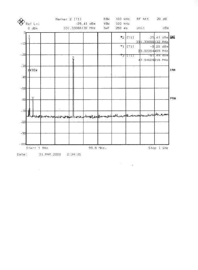
Figure 1. BW=6 MHz input signal Input to ODU from IDU FCC ID: NTTSX1121, NTTSX1122
Contact Information
Applicant
Tim Buchner(Strategic Marketing)
Technical Contact
T.N. Cokenias ConsultingThomas N Cokenias
[email protected]650 726 1263
355 El Granada Blvd · El Granada, California · United States
Non-Technical Contact
T.N. CokeniasThomas N Cokenias
[email protected]650 726 1263
Technical Specifications
| # | Rule Parts | Frequency Range | Power Output | Emission | Tolerance |
|---|---|---|---|---|---|
| 3 | 21 | 2.15 GHz - 2.16 GHz | 4 W | 1M50W7D | 10 ppm |
Other Applications from WJ Communications, Inc.
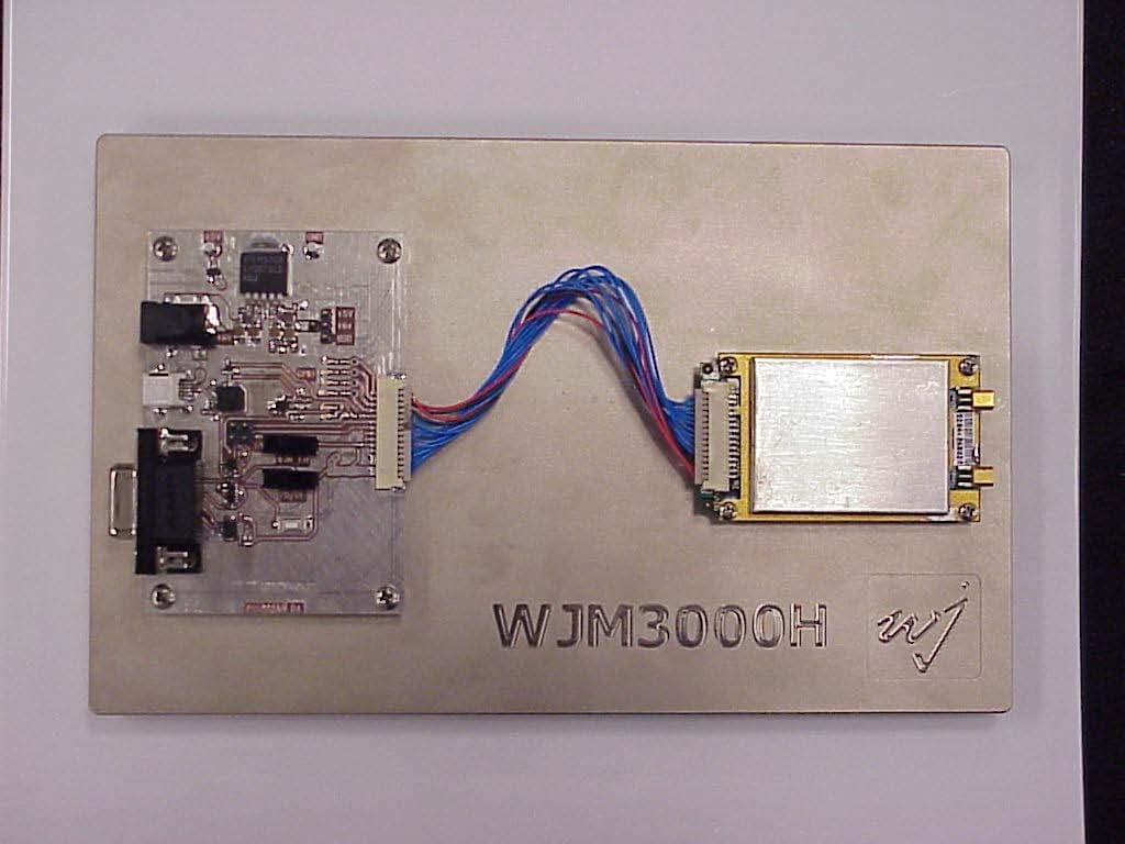
NTTWJM3000
Jan 11, 2007RFID Reader Module
Equipment Class
DSS - Part 15 Spread Spectrum Transmitter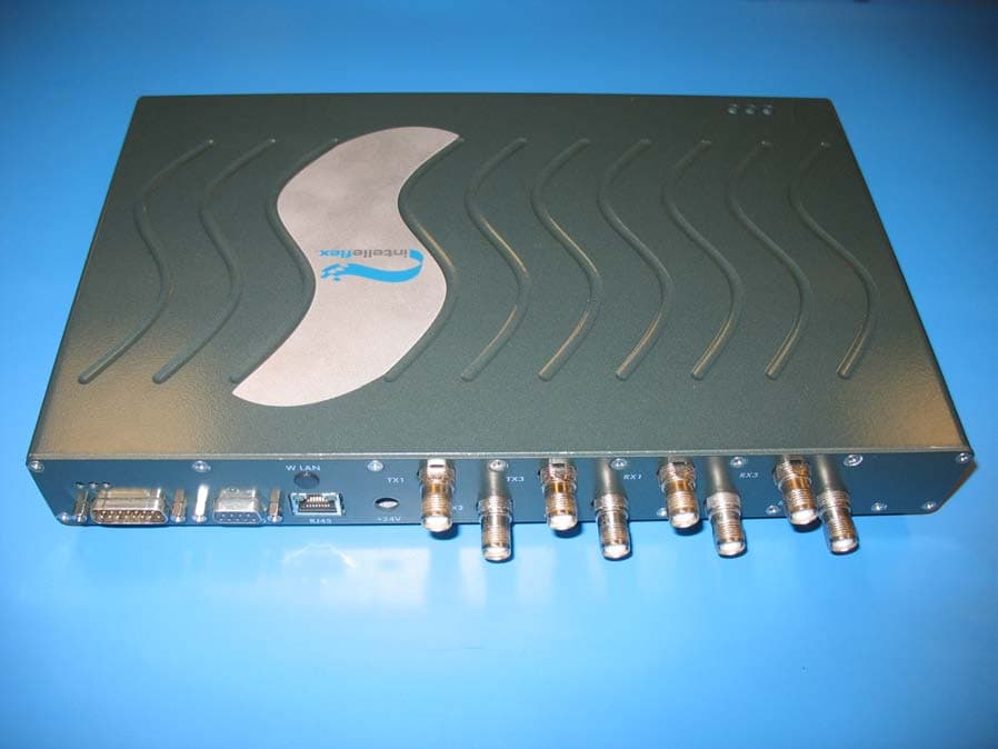
NTTSR320
Jun 20, 2006RFID Tag Reader
Equipment Class
DSS - Part 15 Spread Spectrum Transmitter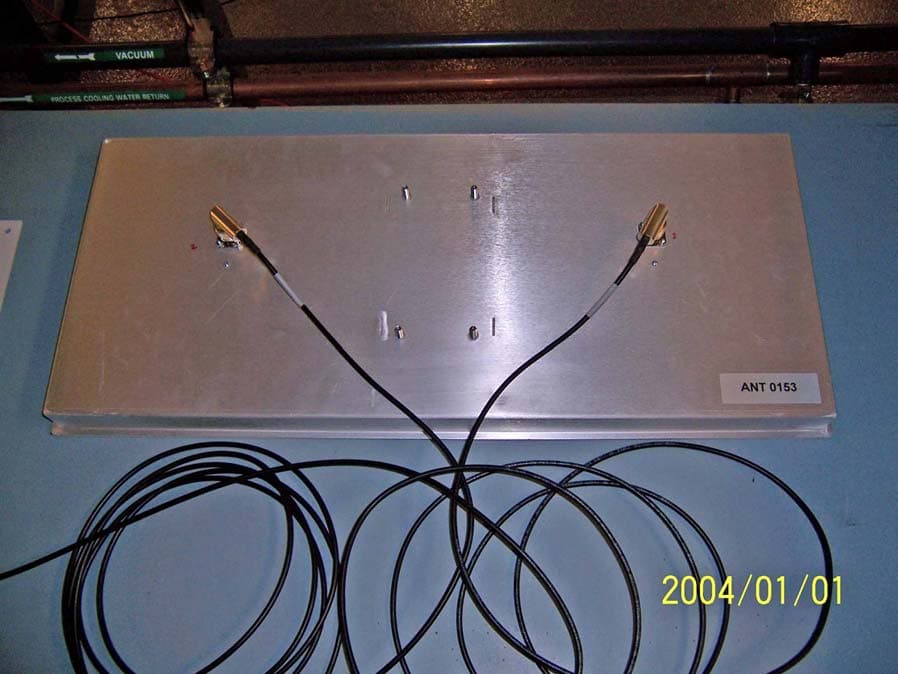
NTTWJSR22XX
Sep 12, 2005902-928MHz RFID Reader
Equipment Class
DSS - Part 15 Spread Spectrum Transmitter
NTTWJMPR7XXX
Dec 12, 2004RFID Reader
Equipment Class
DSS - Part 15 Spread Spectrum Transmitter
NTTWJMPR6XXX
Dec 09, 2004RFID Reader
Equipment Class
DSS - Part 15 Spread Spectrum Transmitter