NTTSX1127UNII Point-to-Multipoint Head End Transceiver
WJ Communications, Inc.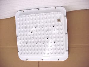
Click to zoom
Application Details
- Equipment Class
- NII - Unlicensed National Information Infrastructure TX
- Date of Grant
- Dec 19, 2000
- Application Purpose
- Original Equipment
- Date of Application
- Sep 19, 2000
- Equipment Note
- UNII Point-to-Multipoint Head End Transceiver
- Frequency Range
- 5773.00000000 - 5823.00000000
- Company
- WJ Communications, Inc.
- Country
- United States
Documents & Files
Document Text
Text extracted from the exhibit documents filed with the FCC. Open a document above to read the original.
Attestation Statements
tel: 650-726-1263 fax: 650-726-1252 internet: [email protected] Thomas N. Cokenias EMC &Radio Approvals Test & Consulting Services for Commercial, Military, International Compliance P.O. Box 1086 El Granada, CA 94018 21 July 2000 FCC Laboratory 7435 Oakland Mills Road Columbia, MD 21046 Attention: Application Examiner Reviewing Engineer Re: Request for confidentiality per Section 0.459 of FCC Rules Applicant: Watkins-Johnson Company FCC ID: NTTSX1127 To whom it may concern, Request is hereby submitted, on behalf of my client Watkins Johnson Co., to withhold from public review certain portions of the application for equipment certification for the referenced FCC identifier. In particular, the following sections of the application and report are requested to be kept confidential: Schematics Block diagrams Theory of operation (P2P/P2MP architechture) Rationale for request for confidentiality: Watkins Johnson has invested considerable time and materials in research and development to produce the referenced product. Disclosure of the confidential portions of this application to competitors would give them competitive advantage in developing similar products. The $135 fee for confidentiality has been submitted along with the fee for certification. If you have questions or need further information, please contact the undersigned. Sincerely, THOMAS N. COKENIAS EMC Consultant/Agent for Watkins Johnson Co. tel: 650-726-1263 fax: 650-726-1252 internet: [email protected]
Cover Letter(s)
tel: 650-726-1263 fax: 650-726-1252 internet: [email protected] Thomas N. Cokenias EMC & Radio Type Approvals Test & Consulting Services for Commercial, Military, International Compliance P.O. Box 1086 El Granada, CA 94018 15 Sept 2000 CCS 1366 Bordeaux Drive Sunnyvale, CA 94087 Attention: Mike Kuo Re: Correction of Information Submitted with TCB Application Applicant: Watkins Johnson FCC ID: NTTSX1127 Dear Mike The original submission indicated testing was performed at Compliance Certification Services in Morgan Hill. The correct location for the radiated (15.205 and 15.107) testing was Cisco Systems, Building 7 EMC chamber. The correct location for conducted measurements (15.407) was Watkins Johnson. I apologize for the error. Best regards Tom Cokenias Agent for Watkins Johnson
External Photos
SX1126 and SX1127 Wireless Transceiver SX1126 Front View with Antenna SX1127 Front View without Antenna Bottom View
Internal Photos
SX1126 SX1127 Open Unit with Cover Board Front Board Front Board Back
Parts List/Tune Up Info
Microwave Band RF Head, CPEPage 1 of 13 . 1.1 Terminology and Abbreviations This section lists and defines commonly used terms and abbreviations. ADCAnalog to Digi tal Converter AGCAutoma tic Gain Control ASICApplication Specific Integrated Circuit BWBandwidth CPECus to mer Pre mise Equip me nt DACDigital to Analog Co nverter dBDecibels DSPDigital Signal Processor (or Processing) EEPROMElectrically Erasable Programmable Read Only Memory FDDFrequency Division Duplexing FECForward Error Correction FLLFrequency Locked Loop FPGAField Programmable Gate Array IDUIn Door Unit IFInter mediate Freq ue ncy IMDIntermodulation Distortion LNALow Noise Amplifier LOLocal Oscillator LPFLow Pass Filter LSBLeast Significant Bit MDSMultipoint Distribution Service MMDSMultichannel Multipoint Distribution Service msMilliseconds MSBMost Significant Bit MspsMega samples per second NPRNoise Power Ratio nsNanoseco nds NVMNon-Volatile Memory (EEPROM) ODUOut Door Unit P2MPPoint to Multi Point P2PPoint to Point PICPeripheral Interface Controller PINP-type Intrinsic N-type (doped semiconductor junction) PLDProgrammable Logic Device PLLPhase Loc ked Loop RxReceive SAWSurface Acoustic Wave (filter) SFDRSpur Free Dynamic Range SINADSignal to Noise and Distortion SNRSignal to Noise Ratio SPISerial Peripheral Interface T/HTrack and Hold THDTotal Harmonic Distortion TxTransmit UARTUniversal Asynchronous Receiver Transmitter UBRUniversal Broadband Router U-NIIUnlicensed National Information Infrastructure VCAVoltage Controlled Attenuator VCXOVoltage Controlled Crystal Oscillator VOFDMVector Orthogonal Frequency Division Multiplexing Microwave Band RF Head, CPEPage 2 of 13 . 2 RF Head Description Figure 1: RF Head Functional Block Diagram - TYPICAL, FOR REFERENCE ONLY 2.1 IF Coaxial Cable One coaxial cable ports is provided on the bottom side of the RF Head. This cable carries the 6 signals from the IDU to the ODU. • -48 V nominal DC voltage (High Power type only). • 24 V nominal DC voltage (Standard Power type only). • 24 MHz low noise frequency reference for the Tx and Rx PLLs • Modulated Tx IF signal, centered at 330 MHz • Modulated Rx IF signal (from ODU to IDU), centered at 426 MHz • Modulated 750 kHz carrier for Serial Communication Channel • Tx blanking signal (48 MHz carrier frequency) 2.1.1 IF Coaxial Cable Connector The IF coaxial connector shall be a weatherized female Type-N on the RF Head 3.0 Operational Modes 3.1 Signal Bandwidths The CPE must support 3 different signal bandwidths for both Tx and Rx operation. The three bandwidths are 1.5, 3.0 and 6 MH z no mi nally. A bandwidth identification signal will be provided through the Serial Communication channel (this feature is currently under review). For channelization plans with channel spacing different than these bandwidths, the signal bandwidth closest to, but not larger than, the channel spacing shall be utilized for that channel spacing. 3.2 Tx Gain Control CPE Tx gain is controlled by the Hub Receiver. The Tx chain behaves as a linear programmable gain amplifier. The Tx power is a product of the Tx IF input signal and ODU Tx gain. Tx gain is set in response to the IDU host gain set command through the Serial Communication Channel. Calibration of the variable attenuator (if required) is performed during manufacturing and correction data is stored in the ODU NVM. The modulated Tx signal must meet all S/N specifications over the full Tx power range. The entire gain control range of the Tx consists of a variable gain control and a fixed gain control step. Note that the high power CPEs and the millimeter-wave CPEs do not have a fixed gain control step. The state of the fixed gain control step is determined by proximity to the HUB receiver and is set appropriately at installation. It does not change during operation of the radio. The variable gain is controlled by the Hub Receiver and can be changed at any time. Implementation of the variable gain attenuator can be a continuously variable attenuator or a step attenuator with minimum step size of 1 dB. The total gain control required for the standard power head is comprised of a fixed attenuation and a variable attenuation. For example, for the GHz band, the total gain control is 77 dB (3 MHz BW), which is comprised of 25 dB of fixed attenuation and 52 dB of variable attenuation. The maximum value of fixed attenuation is 25 dB and the minimum value is 0 dB. The Microwave Band RF Head, CPEPage 3 of 13 . fixed attenuation feature is required for the GHz band only. The amount of variable gain control varies with signal BW. The 6 MHz BW requires 3 dB less variable gain control, and the 1.5 MHz BW requires 3 dB more variable gain control. 3.3 Tx Power Blanking The CPE Tx chain will be instructed to blank when it is not actually transmitting data. This is to prevent overloading the Hub Receiver with aggregate noise power from multiple CPEs having high Tx chain noise/gain products. The blanking command will be derived in the IDU. The Tx power amplifier chain must be sufficiently blanked to minimize excessive noise from being transmitted when in this mode. 3.4 Tx Power Maximum Threshold Detector The output power of the Tx chain is monitored to insure that it does not exceed a pre-determined maximum output power. If the Tx power exceeds this level, than the Tx chain is blanked. The maximum threshold is set based on the signal bandwidth setting. 3.5 Rx Gain Control Rx gain control consists of a fixed gain control step and a continuously variable control or Rx AGC. The state of the fixed gain control step is determined by proximity to the HUB receiver and is set appropriately at installation. Only the standard power CPE utilizes the fixed gain step. Note that the high power CPEs and the millimeter-wave CPEs do not have a fixed gain step. The Rx AGC level is set by commands from the IDU DSP. The requirement is to have ‘transient-free’ gain adjustments as to prevent glitches on the Rx signal from affecting the DSP. As such, …
Text truncated - open the document above for the full version.
RF Exposure Info
Sheet1 Watkins JohnsonUNII TransceiverFCC ID: NTTSX1127 Calculate mW/cm2 here. Enter freque n RF Hazard Distance Calculation Calculation of Limits from 1.1310 Tab l ControlledAve 6 min mW/cm2 from Table1: 1.00 F(MHz) Actual F, MHz Occ, mW/c2 0.3-3 1 100.0 Max RF Powe TX Antenna MPE 3.0 - 30.0 30 30.0P, dBm G, dBi Safe Distance, cm 30.0-300 20 1.0300-1500 454 1.5 13.3 17.5 9.8 1500-100000 1500 5.0 15.0 8.0 4.0 0.0 0.0 0.30.0 0.0 0.30.0 0.0 0.3 Enter P(wat t Equivalent dBm 0.0 0.0 0.30.0 0.0 0.30.0 0.0 0.30.0 0.0 0.3 Basis of Calculations: 2 33.0E^2/3770 = S, mW/cm2E, V/m = (Pwatts*Ggain*30)^.5/d, metersd = ((Pwatts*G*30)/3770*S))^0.5 Pwatts*Ggain = 10^(PdBm-30+GdBi)/10)NOTE: For mobile or fixed location transmitters, minimum separation distance is 20 cm, even if calculations indicate MPE distance is less Page 1 Sheet1 n cy in MHz: l e 1 UncontrolledAve 30 min Gen, mW/cm2 100.0 6.00.20.31.0 Page 2
RF Exposure Info
Table 3. Antenna Radiation Hazard Max Power Output, dBmAntenna gain, dBiMPE distance, cm SX1126A: 1922.533.5 SX1127: 13.317.520.0 15.08.020.0
Test Report
Results of FCC Testing for the SX1127 UNII Head End Transceiver August 7, 2000 Jay KruseWJ Communications Alberto CamposWJ Communications Tom Coke niasCo ns ulta nt A SX1127 UNII Head End (HE) transceiver was tested for maximum power spectral density, maximum output power, and maximum bandedge emissions. Based on consultation with Greg Czumak at the FCC (11/5/99), the following methods were developed for testing U-NII transceivers (Point to Multi-Point Transceivers): Peak Power Spectral Density17 dBm/MHz – (Antenna Gain-6) (if Antenna Gain ≥ ≥≥ ≥ 6 dBi) 17 dBm/MHz (if Antenna Gain < 6 dBi) Resolutio n Ba ndwidth = 1MHz Video Bandwidth = 1 MHz Average = 100 sweeps Peak Search Measure Peak Peak Transmit Power17 dBm/MHz + 10*Log(BW) MHz – (Antenna Gain-6) (if Antenna Gain ≥ ≥≥ ≥ 6 dB i) 17 dBm/MHz + 10*Log(BW ) MHz (if Antenna Gain < 6 dBi) Resolution Bandwidth ~ 1% Emission Bandwidth Video Bandwidth = Resolution Bandwidth Set Channel Bandwidth = Emission Bandwidth View Trace Measure Power i n C ha nnel Ba ndwi dt h Band Edge-17 dBm/MHz – Antenna Gain (Bandedge) -27 dBm/MHz – Antenna Gain (Bandedge ± 10 MHz) Resolution Bandwidth ~ 1% Emission Bandwidth Video Bandwidth = Resolution Bandwidth/30 Center Frequency = Band Edge Set Adjacent C hannel Bandwidth = 1 MHz View Trace Measure Power i n Adjacent C hannel Bandwidth Unit # 21500310002 was measured using the above methods. The power of the Orthogonal Frequency Division Multiplex (OFDM) input signal was –17 dBm. A block Diagram of the measurement setup is shown in Figure 1. The frequency range of the unit is from 5773 MHz to 5823 MHz and therefore the worse case bandedge emmisions occur at the high end of the band. Tables 1 through 6 summarize the FCC limits and the measured results. The HE will be used with two antennas: an 8 dBi Omnidirectional antenna and a 17.5 dBi sector antenna. The bandwidth of the OFDM signal was 6 MHz. Laptop Computer R&S FSIQ-26 Spectrum Analyzer Tektronix AWG2021 Arbitrary Waveform Generator Modem WJ Communications Upconverter WJ Communications IF Quadraplexer and 24 MHz Reference Generator Directional Coupler Agilent 331 Power Meter DC Power Supply WJ Communications Tranceiver Step Attenuator Figure 1. Block diagram of measurement setup. Table 1. High Band data for Peak Spectral Density and Peak Transmit Power. Antenna Gain (dBi) Maximum Allowed PSD (dBm/MHz) Measured PSD (dBm/MHz) Maximum Allowed Peak Transmit Power (dBm) Measured Peak Transmit Power (dBm) 17.55.55.513.313.3 8157.222.815.0 Table 2. High Band data for Band Edge Emmissions. Antenna Gain (dBi) Maximum Allowed Bandege PSD (dBm/MHz) 5825 MHz Maximum Measured BandedgePSD (dBm/MHz) 5825 MHz Maximum Allowed Bandege PSD (dBm/MHz) 5835 MHz Maximum Measured BandedgePSD (dBm/MHz) 5835 MHz 17.5-34.5-41.1-44.5-68.0 8-25.0-39.0-35.0-67.4 Table 3. Mid Band data for Peak Spectral Density and Peak Transmit Power. Antenna Gain (dBi) Maximum Allowed PSD (dBm/MHz) Measured PSD (dBm/MHz) Maximum Allowed Peak Transmit Power (dBm) Measured Peak Transmit Power (dBm) 17.55.55.513.313.3 8157.222.815.0 Table 4. Mid Band data for Band Edge Emmissions. Antenna Gain (dBi) Maximum Allowed Bandege PSD (dBm/MHz) 5825 MHz Maximum Measured BandedgePSD (dBm/MHz) 5825 MHz Maximum Allowed Bandege PSD (dBm/MHz) 5835 MHz Maximum Measured BandedgePSD (dBm/MHz) 5835 MHz 17.5-34.5-65.6-44.5-65.1 8-25.0-65.2-35.0-64.2 Table 5. Low Band data for Peak Spectral Density and Peak Transmit Power. Antenna Gain (dBi) Maximum Allowed PSD (dBm/MHz) Measured PSD (dBm/MHz) Maximum Allowed Peak Transmit Power (dBm) Measured Peak Transmit Power (dBm) 17.55.55.513.313.3 8157.222.815.0 Table 6. Low Band data for Band Edge Emmissions. Antenna Gain (dBi) Maximum Allowed Bandege PSD (dBm/MHz) 5825 MHz Maximum Measured BandedgePSD (dBm/MHz) 5825 MHz Maximum Allowed Bandege PSD (dBm/MHz) 5835 MHz Maximum Measured BandedgePSD (dBm/MHz) 5835 MHz 17.5-34.5-65.4-44.5-65.1 8-25.0-64.3-35.0-65.5 Ba ndw idth =6.0 MHz Pout= 13.3 dBm Hig h Ba nd Maximum Power Spectral Density = 5.5 dBm/MHz Maximum Transmit Output Power = 13.3 dBm Ba ndw idth =6.0 MHz Pout= 13.3 dBm Hig h Ba nd P 5725 MHz = -41.1 dBm/MHz P 5715 MHz = -68.0 dBm/MHz Ba ndw idth =6.0 MHz Pout= 15.0 dBm Hig h Ba nd Maximum Power Spectral Density = 7.2 dBm/MHz Maximum Transmit Output Power = 15.0 dBm Ba ndw idth =6.0 MHz Pout= 15.0 dBm Hig h Ba nd P 5725 MHz = -39.0 dBm/MHz P 5715 MHz = -67.4 dBm/MHz Ba ndw idth =6.0 MHz Pout= 13.3 dBm Mid Band Ba ndw idth =6.0 MHz Pout= 15.0 dBm Mid Band Ba ndw idth =6.0 MHz Pout= 13.3 dBm Low Band Ba ndw idth =6.0 MHz Pout= 15.0 dBm Low Band
Test Report
Amendment to the Results of FCC Testing for the SX1127 UNII Head End Transceiver Additional Testing of Peak Power as a Function of Resolution Bandwidth December 18, 2000 Jay Kr useWJ Co mmunicatio ns To m Co ke niasCons ulta nt This document is an amendment to the document dated August 7, 2000 describing the FCC test results on the WJ Communications SX1127 UNII Head End Transceiver. The data illustrates the affect of reducing the resolution bandwidth of the spectrum analyzer to determine the peak transmit power output of the transceiver. It should be noted that the peak transmit power used in the original submittal was determined by the following criteria developed by Greg Czumak at the FCC (11/5/99): 1. Resolution Bandwidth ~ 1% Emission Bandwidth 2. Video Bandwidth = Resolution Bandwidth 3. Set Channel Bandwidth = Emission Bandwidth 4. View Trace 5. Measure Power in Channel Bandwidth The data show n below uses the following method: 1. Resolution Bandwidth ~ Emission Bandwidth 2. Video Bandwidth (VB) = Resolution Bandwidth (RB) 3. Trace was averaged using a Max Peak Detector 4. View Trace 5. Resolution Bandwidth = Video Bandwidth = 1 MHz 6. Trace was averaged using a Max Peak Detector 7. View Trace 8. Compare maximum values (Delta not to be greater than 13 dB.) Figure 1. Bandwidth = 6 MHz, Pout = 15 dBm Top Trace: RB = VB = 10 MHz Bottom Trace: RB = VB = 1 MHz Delta = 9.4 dB Figure 2. Bandwidth = 3 MHz, Pout = 15 dBm Top Trace: RB = VB = 3 MHz Bottom Trace: RB = VB = 1 MHz Delta = 4.0 dB Figure 3. Bandwidth = 1.5 MHz, Pout = 15 dBm Top Trace: RB = VB = 2 MHz Bottom Trace: RB = VB = 1 MHz Delta = 2.0 dB
Contact Information
Applicant
Tim Buchner(Strategic Marketing)
Technical Contact
T.N. Cokenias ConsultingThomas Cokenias
[email protected]650-726-1263
355 El Granada Blvd. · El Granada, California · United States
Test Firm
Cisco Systems, Inc.Daisy Poon
Technical Specifications
| # | Rule Parts | Frequency Range | Power Output |
|---|---|---|---|
| 1 | 15E | 5.77 GHz - 5.82 GHz | 31.60 mW |
Other Applications from WJ Communications, Inc.
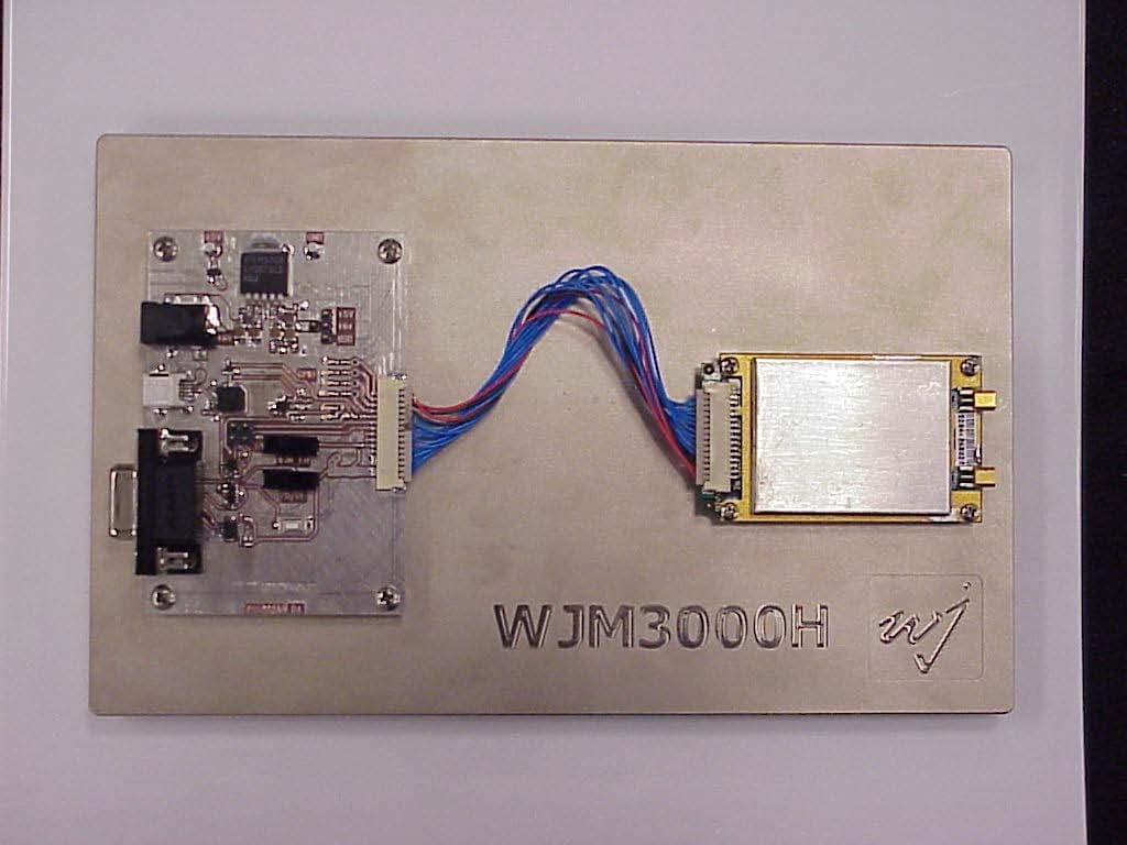
NTTWJM3000
Jan 11, 2007RFID Reader Module
Equipment Class
DSS - Part 15 Spread Spectrum Transmitter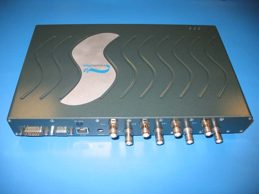
NTTSR320
Jun 20, 2006RFID Tag Reader
Equipment Class
DSS - Part 15 Spread Spectrum Transmitter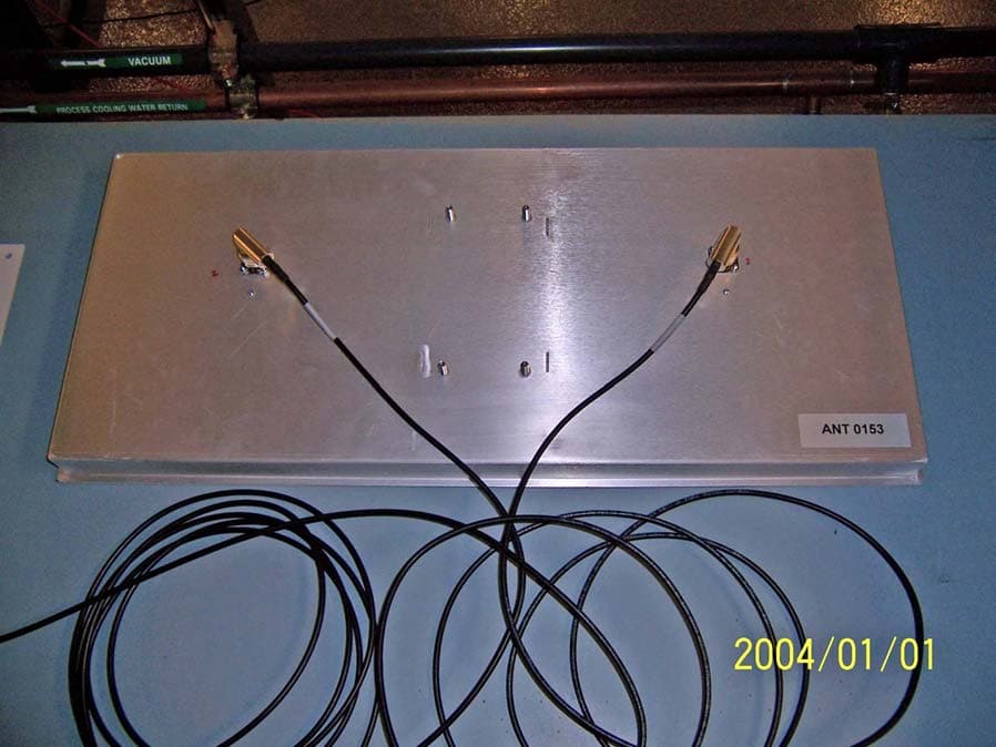
NTTWJSR22XX
Sep 12, 2005902-928MHz RFID Reader
Equipment Class
DSS - Part 15 Spread Spectrum Transmitter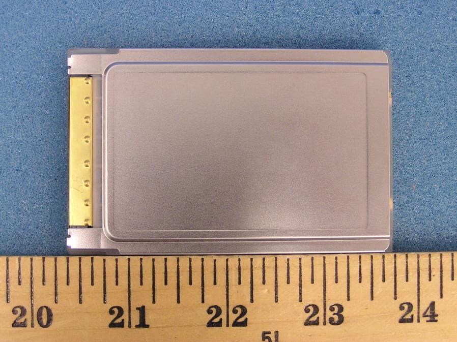
NTTWJMPR7XXX
Dec 12, 2004RFID Reader
Equipment Class
DSS - Part 15 Spread Spectrum Transmitter
NTTWJMPR6XXX
Dec 09, 2004RFID Reader
Equipment Class
DSS - Part 15 Spread Spectrum Transmitter