NVJAR5000AAR5000A+3B Communications Receiver
AOR USA Inc.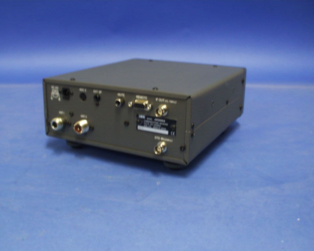
Click to zoom
Application Details
- Equipment Class
- CSR - Scanning Receiver
- Date of Grant
- May 31, 2004
- Application Purpose
- Original Equipment
- Date of Application
- May 31, 2004
- Equipment Note
- AR5000A+3B Communications Receiver
- Frequency Range
- 894.00000000 - 960.00000000
- Company
- AOR USA Inc.
- Country
- United States
Documents & Files
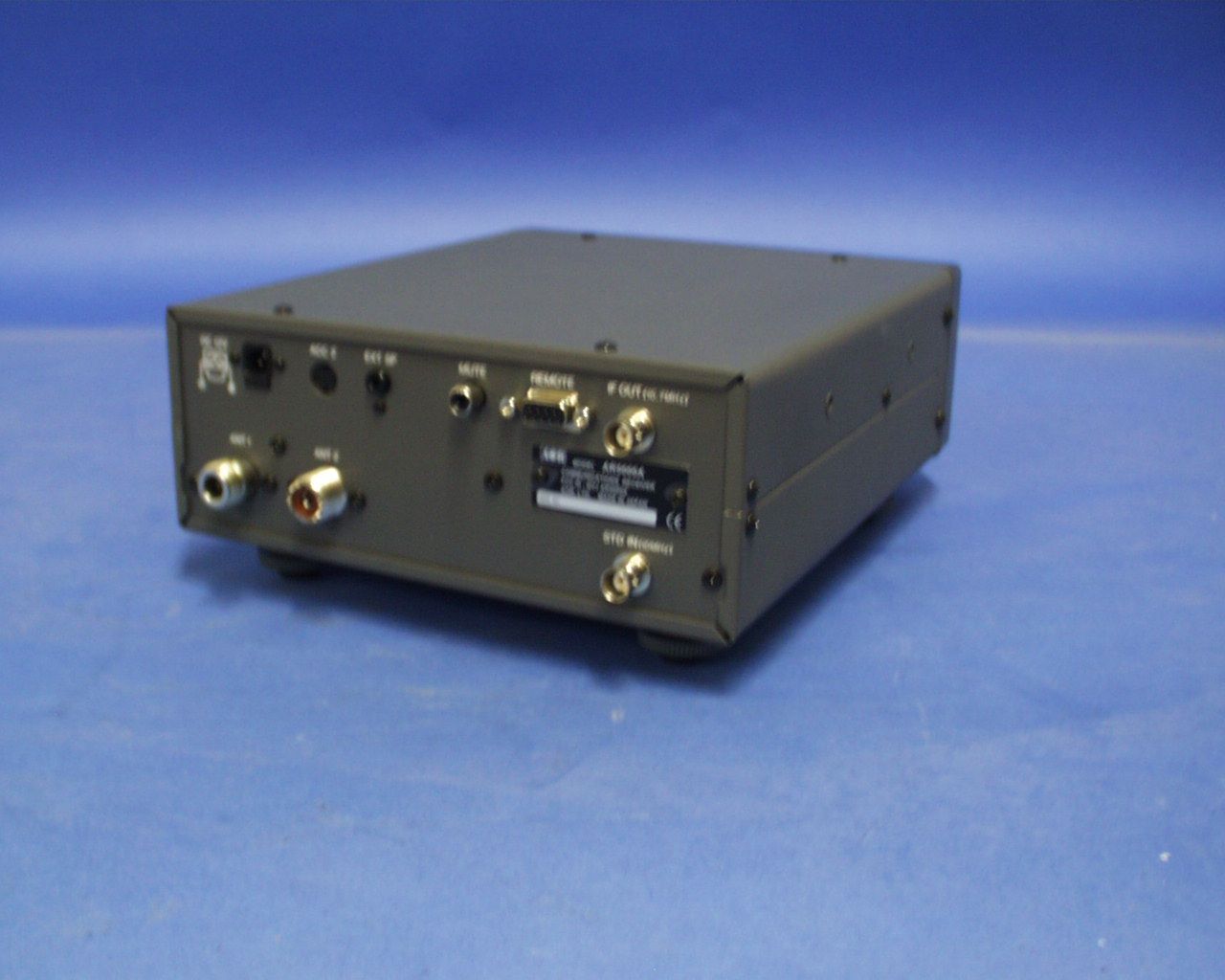
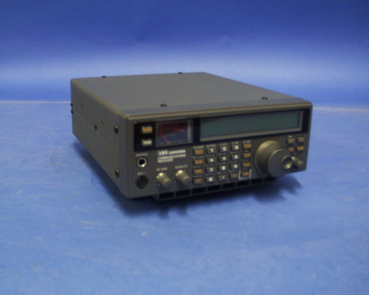
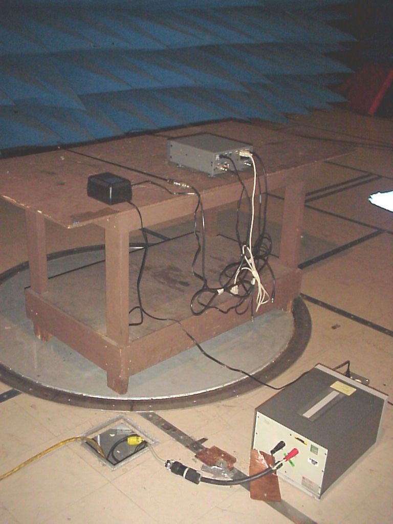
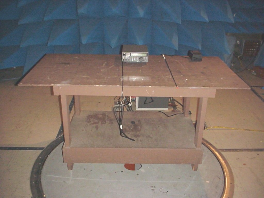
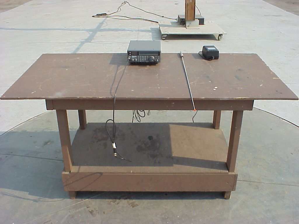
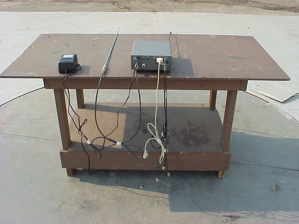
Document Text
Text extracted from the exhibit documents filed with the FCC. Open a document above to read the original.
Users Manual
Addendum Note: This equipment has been tested and found to comply with the limits for a Class B digital device, pursuant to part 15 of the FCC Rules. These limits are designed to provide reasonable protection against harmful interference in a residential installation. This equipment generates, uses and can radiate radio frequency energy and, if not installed and used in accordance with the instructions, may cause harmful interference to radio communications. However, there is no guarantee that interference will not occur in a particular installation. If this equipment does cause harmful interference to radio or television reception, which can be determined by turning the equipment off and on, the user is encouraged to try to correct the interference by one or more of the following measures: --Reorient or relocate the receiving antenna. --Increase the separation between the equipment and receiver. --Connect the equipment into an outlet on a circuit different from that to which the receiver is connected. --Consult the dealer or an experienced radio/TV technician for help. Changes or modifications not expressly approved by the party responsible for compliance could void the user's authority to operate the equipment No special accessories are required in order for the device to comply with the applicable requirements. WARNING: Modification of this device to receive cellular radiotelephone service signals is prohibited under FCC rules and Federal law.
Users Manual
AR5000 OPERATING MANUAL PAGE 1 Contents (1) Table of contents .......................................................................... 1 (2) Introduction ................................................................................... 2 2-1 Key information and common menus .................................. 3 2-2 Accessories supplied .......................................................... 4 (3) Major Features .............................................................................. 4 (4) Precautions ................................................................................... 4 4-1 Location .............................................................................. 4 4-2 Looking after your receiver ................................................... 5 4-3 Power requirements ............................................................ 5 4-4 Aerial (antenna) connection ................................................. 5 (5) Controls and functions ................................................................ 6 Front panel 5-1 On/Off power switch ............................................................ 6 5-2 S-meter (signal strength meter) ........................................... 6 5-3 Liquid Crystal Display (LCD) ................................................ 6 5-4 Main (large) rotary tuning control - MAIN DIAL .......................... 8 5-5 Sub (small) rotary tuning control - SUB DIAL ............................ 8 5-6 Torque adjustment (MAIN DIAL brake) ..................................... 8 5-7 Removable feet ................................................................... 9 5-8 Internal speaker .................................................................. 9 5-9 SQ - squelch control (plus RF control) ................................. 9 5-10 Volume control (AF GAIN) ................................................. 10 5-11 ACC 1 accessory number one socket ................................ 10 5-12 Headphone socket ............................................................. 10 5-13 Front panel keys ................................................................ 10 Rear panel 5-14 DC 12V - external power connection .................................. 15 5-15 ACC 2 (accessory 2 socket) ............................................. 15 5-16 EXT SP - external speaker output socket ........................... 16 5-17 REMOTE - RS232C computer control port ........................ 16 5-18 I.F. OUTPUT (10.7 MHz) ................................................... 16 5-19 STD IN (10 MHz) ............................................................... 16 5-20 MUTE ............................................................................... 16 5-21 ANT 2 ............................................................................... 17 5-22 ANT 1 ............................................................................... 17 (6) Basic manual operation of the receiver ..................................... 17 6-1 Switching on for the first time .............................................. 17 6-2 Changing VFO .................................................................... 17 6-3 Tuning the receiver using the rotary controls ........................ 18 6-4 Entering a frequency via the numeric keypad ....................... 18 6-5 Correction of frequency input via the numeric keypad ........... 19 6-6 Selecting tuning step (increment) ......................................... 19 6-7 Step-adjust .......................................................................... 20 6-8 FREQUENCY OFFSET ....................................................... 22 6-9 Changing receive mode (AUTOMODE) ................................ 22 6-10 IF BANDWIDTH ................................................................ 24 6-11 AF SET - (Audio characteristics) ........................................ 25 6-12 Audio tone eliminator (T-ELMT) ......................................... 27 6-13 DTMF decoder .................................................................. 28 6-14 RF Attenuator & preamplifier ............................................. 28 6-15 CONFIG menu outline of facilities ...................................... 28 6-16 CONFIG - LAMP ............................................................... 29 6-17 CONFIG menu - BEEP ..................................................... 29 6-18 CONFIG - EXTERNAL I.F. output (SDU5000) ..................... 29 6-19 CONFIG - Computer control BPS ....................................... 29 6-20 CONFIG - Advanced aerial switching .................................. 30 6-21 CONFIG - Frequency standard ............................................ 32 (7) Memory banks & channels ............................................................ 33 7-1 Storing receive data into memory - VFO mode ...................... 33 7-2 Memory recall - Recalling receive data from memory ............. 34 7-3 Transfer of memory channel to VFO ...................................... 35 7-4 Changing and deleting memory data ..................................... 35 7-5 Deleting memory channels and banks ................................... 36 (8) SCAN - scanning memory channels & banks ............................. 37 8-1 SCAN - outline introduction to facilities available ................... 37 8-2 Starting to SCAN, considerations .......................................... 37 8-3 SCANNING a memory bank ................................................. 38 8-4 Selecting a single memory bank to scan ................................ 38 8-5 Memory bank linking to scan ALL memory banks .................. 39 8-6 Specifying memory bank linking ............................................ 39 8-7 Scanning a memory bank which is not linked ........................ 39 8-8 SCAN channel PASS (lockout) .............................................. 40 8-9 Cyber Scan in SCAN mode .................................................. 41 (9) Additional SCAN facilities…
Text truncated - open the document above for the full version.
Attestation Statements
May 27, 2004 To whom it may concern, RE: FCCID: NVJAR5000A Manufacturer’s ID: AR5000A+3B The CPU of the AR5000A+3B has been specially designed and programmed for the US domestic market, in compliance with the above regulation. As such, there is no frequency data for the US Cellular frequency band in the processor’s programmed data. The CPU is not field programmable, so it cannot be modified by the consumer. If an operator tries to enter a cellular frequency into the receiver by means of the tuning controls, keypad entry or via PC through the RS-232C serial port, those entries will be automatically ignored (and rejected). In combination with the above comments, it is just not possible to enable cellular frequency reception through any of the physical modification means described in the regulation, specifically “by clipping the leads of, or installing, a simple component such as a diode, resistor or jumper wire; replacing a plug-in semiconductor chip; or programming a semiconductor chip using special access codes or an external device, such as a personal computer.” The Band Pass Filters of the AR5000A+3B have no adjustable components (such as variable capacitors or pots), therefore, no readjustments of the manufactured values are possible. Also, there are a significant number of small SMD capacitors used in the circuit. Their presence makes it extremely difficult to alter its characteristics of the receiver. These components are not readily accessible elements in the product. Near total disassembly of the receiver, including the removal of sub-boards from the main circuit board, is necessary to gain access to the described components, which are on the rear part of the circuit board if the unit is disassembled in the conventional manner. It is also quite likely that any attempts to modify these (BPF) circuits of the receiver would result in damage and/or a serious degradation of the receiver’s performance We certify the referenced receiver is in compliance with all the applicable regulations contained in the section Sincerely, Takashi “Taka” Nakayama Vice President AOR USA, Inc.
Cover Letter(s)
From: [email protected] Sent: Thursday, May 27, 2004 4:46 PM To: [email protected] Subject: Response to Correspondence Ref # E04-000041-1 All non-comformities have been addressed. Item 1. A signed CKC CS general agreement has been faxed to you. Item 2. An exhibit has been uploaded to address this item. Refer to exhibit described as Theory of Operation. Item 3. Refer to the new test report exhibit, which has been uploaded. Item 4. No action was required for this item. Item 5. An exhibit has been uploaded to address this item. Refer to exhibit described as FCC Labelling. Items 6, 7, & 8. An exhibit has been uploaded to address all these items. Refer to exhibit described as User's Manual Addendum. Item 9. An exhibit has been uploaded to address this item. Refer to the test report exhibit described as Signal Rejection Test Data. In addition, the manufacturer has provided a letter attesting to the fact that the unit does not receive Cellular Radiotelephone Service Signals and that it cannot be modified to do so. Refer to the Cover Letter Exhibit. Thank You
ID Label/Location Info
FCC ID Label: FCC ID: NVJAR5000A FCC ID Label Placement: Label Location
ID Label/Location Info
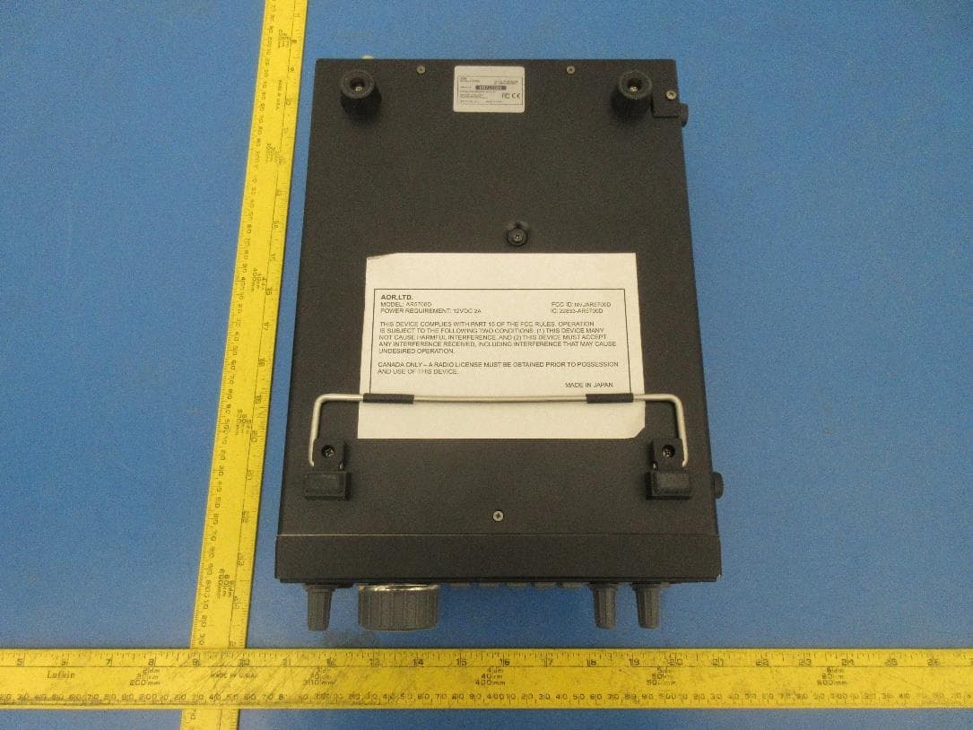
The following pictures are the labels that will be affixed on the device. FCC ID Label (Ref §2.925(a)) Compliance Statement Label (Ref §15.19(a)(3)) and Scanning Receiver Warning Label (Ref §15.121(f))
Parts List/Tune Up Info
AFC UNIT Part Used PartType Designators ------------------------------------------------------------------------ 1 1 15pF (Cer) C1 2 1 100pF(Cer UJ) C5 3 1 150pF(Cer) C15 4 1 270pF(Cer UJ) C4 5 1 330pF(Cer UJ) C2 6 2 1nF (Cer) C11 C13 7 2 10nF (Cer) C6 C12 8 3 0.1uF (Cer) C3 C9 C14 9 1 2.2uF/16V (Tan) C8 10 1 4.7uF/6.3V(Tan) C7 11 1 10uF/6.3V (Os) C10 12 2 100 R11 R12 13 1 470 R6 14 3 4.7K R7 R14 R15 15 2 6.8K R3 R4 16 2 10K R2 R13 17 1 39K R9 18 1 47K R5 19 1 56K R8 20 1 100K R10 21 2 KE-04980 T1 T2 22 1 2SK160 Q1 23 1 TC4W53F IC1 24 1 MC3372M IC2 25 1 uPC358G IC3 or TA75358F or NJM2904M 26 1 PI28A10M J1 ACC1 UNIT Part Used PartType Designators ------------------------------------------------------------------------ 1 1 TCS7932-18-201 J1 CPU UNIT Part Used PartType Designators ------------------------------------------------------------------------ 1 1 10pF(Cer) C65 2 1 20pF(Cer) C23 3 1 20pF(CV05D2001) TC1 4 2 33pF(Cer) C22 C24 5 34 101 (Cer) C6 C7 C15 C16 C17 C18 C19 C20 C21 C26 C27 C28 C29 C33 C34 C35 C36 C37 C38 C40 C41 C42 C43 C44 C45 C46 C47 C48 C49 C53 C54 C64 C77 C80 6 24 102 (Cer) C1 C2 C3 C4 C5 C8 C9 C10 C11 C12 C13 C14 C30 C31 C32 C39 C50 C51 C52 C58 C63 C67 C70 C78 7 6 0.1uF(Cer) C59 C60 C61 C62 C69 C71 8 4 100uF/10V (Ele) C73 C74 C75 C79 9 1 470uF/6.3V(Ele) C72 10 1 10 R20 11 1 1K R10 12 4 33K R70 R71 R72 R73 13 19 100K R4 R9 R13 R14 R15 R16 R17 R18 R19 R56 R57 R59 R60 R61 R62 R63 R64 R65 R69 14 8 220K R1 R2 R3 R5 R6 R7 R8 R12 15 1 560K R58 16 55 BLM21A121 L5 L6 L7 L8 L9 L10 L11 L12 L14 L15 L16 L17 L18 L19 L20 L21 L22 L23 L24 L25 L26 L27 L28 L29 L30 L31 L32 L33 L34 L35 L36 L37 L38 L39 L40 L41 L42 L43 L47 L48 L49 L50 L51 L52 L53 L54 L55 L56 L57 L58 L59 L60 L61 L62 L63 17 3 HN2D01F D1 D2 D5 18 2 RB500V-40 D3 D4 19 1 DTC323TK Q1 20 1 S-8052HNM IC1 21 1 TC4W66F IC2 22 1 uPD74HC373GS IC5 or TC74HC373AF 23 1 uPD78P064GF IC3 24 1 uPD16430AGF IC4 25 1 32.768Kz X1 26 1 4.9152MHz X2 27 1 D2213 BL1 28 1 DLC-3069PYNGF LCD1 29 25 SKHHBV S2 S3 S4 S5 S6 S7 S8 S9 S10 S11 S12 S13 S14 S15 S16 S17 S18 S19 S20 S21 S22 S23 S24 S25 S26 30 1 SKHHBY S1 31 1 SKHLAC S27 32 1 PI28A02M J8 33 1 PI28A05M J3 34 1 PI28A06M J2 35 1 PI28A09M J5 36 1 PI28A10M J6 37 1 PI28A11M J4 38 1 PI28A13M J1 39 1 PI28G15M J7 40 1 Wire-No.31 JP1 41 1 Wire-No.32 JP2 42 1 Wire-No.33 JP3 POWER UNIT Part Used PartType Designators ------------------------------------------------------------------------ 1 8 0.1uF(Cer) C1 C3 C13 C14 C16 C17 C21 C22 2 2 10uF/16V (Ele) C2 C15 3 3 100uF/10V (Ele) C5 C9 C10 4 2 100uF/16V (Ele) C11 C12 5 2 100uF/10V (Os) C7 C20 6 1 150uF/16V (Os) C4 7 2 220uF/35V (Ele) C18 C19 8 2 2200uF/16V(Ele) C6 C8 9 1 3.3 R9 10 1 2.2K R6 11 2 4.7K R7 R8 12 1 10K R4 13 1 22K R1 14 1 33K R5 15 2 47K R2 R3 16 3 220uH(Rad) L1 L2 L3 17 1 220uH L4 18 2 1S2837 D1 D3 19 1 3GWJ42 D2 20 1 2SB624 Q3 21 1 2SJ330 Q1 22 2 DTA123YK Q4 Q5 23 1 DTC124EK Q2 24 1 S-80840ANUP IC1 25 2 S-81252SGUP IC4 IC5 26 1 TA79L05F IC6 27 1 KPL108 IC2 28 1 KPL130 IC3 29 1 FUSE2A FH1 30 1 PI22A02M J4 31 1 PI22A05M J2 32 1 PI22A06M J1 33 1 PI22A07M J3 34 1 PI22A08M J7 35 1 PI22A09M J5 36 1 PI28A09M J6 37 1 Wire-No.35 JP1 38 1 Wire-No.34 JP2 AUDIO UNIT Part Used PartType Designators ------------------------------------------------------------------------ 1 2 36pF (Cer) C8 C9 2 1 100pF(Cer) C50 3 3 330pF(Cer) C12 C21 C49 4 1 1.8nF (Cer) C45 5 1 5.6nF (Cer) C39 6 19 10nF (Cer) C3 C4 C5 C6 C7 C14 C15 C17 C18 C19 C23 C24 C25 C46 C51 C52 C59 C60 C63 7 1 22nF (Cer) C40 8 12 0.1uF(Cer) C1 C2 C10 C11 C13 C20 C22 C26 C42 C47 C57 C58 9 3 1uF/16V (Tan) C31 C61 C62 10 6 2.2uF/6.3V (Tan) C29 C30 C32 C41 C43 C44 11 2 4.7uF/6.3V (Tan) C27 C48 12 1 10uF/6.3V (Tan) C28 13 4 10uF/16V (Ele C36 C53 C54 C56 14 3 100uF/16V (Ele) C34 C35 C55 15 2 470uF/16V (Ele) C37 C38 16 2 470 R13 R46 17 7 1K R1 R7 R9 R18 R19 R40 R43 18 1 1.5K R31 19 1 2.2K R48 20 1 5.6K R47 21 4 10K R5 R12 R16 R29 22 5 22K R4 R15 R32 R33 R34 23 1 33K R44 24 7 47K R6 R23 R24 R25 R26 R27 R28 25 6 100K R2 R17 R22 R35 R41 R45 26 2 220K R30 R36 27 1 330K R20 28 2 470K R10 R11 29 1 560K R21 30 1 1S2837 D1 31 1 ND411G-1 D2 32 2 RB500V-40 D3 D4 33 1 2SK160 Q2 34 2 2SK680 Q1 Q7 35 1 FMC5 Q5 36 1 TC4S81F IC13 37 1 TC4SU69F IC6 38 2 TC4W53F IC1 IC3 39 1 uPC358G IC9 or TA75358F or NJM2904M 40 2 uPC4570G IC5 IC10 or NJM2043M 41 1 LA4425A IC4 42 1 LC73881M IC12 43 1 AQV212A IC8 44 1 BA1604F IC11 45 1 BH3532FS IC2 46 1 CSA4.19MG CX1 or CSALA4M19G55-B0 47 1 PI22A02M J3 48 1 PI22A03M J2 49 1 PI22A04M J1 50 1 PI22A05M J5 51 1 PI28A03M J6 52 1 PI28A07M J7 53 1 PI28A08M J8 54 1 PI28A13M J4 55 1 Wire-No.64 JP1 56 1 Wire-No.38 JP2 VR UNIT Part Used PartType Designators ------------------------------------------------------------------------ 1 1 10KC(RK0971110-10KC) VR2 2 1 50KA(RK0971110-50KA) VR1 3 1 PI28B06M J1 CPUSUB UNIT Part Used PartType Designators ------------------------------------------------------------------------ 1 5 0.1uF (Cer) C2 C4 C5 C6 C7 2 1 100uF/10V(Ele) C1 3 1 0.47F/5.5V(Ele) C3 4 1 10 R1 5 2 10K R4 R5 6 2 100K R2 R3 7 1 HN58C1001FP-15 IC3 8 1 TC4SU69F IC4 9 2 uPD74HC373GS IC1 IC2 or TC74HC373AF 10 1 PI28A15M J1 CTCSS UNIT(NIS-158) Part Used PartType Designators ------------------------------------------------------------------------ 1 2 18pF (Cer) C7 C8 2 1 82pF (Cer) C3 3 1 100pF(Cer) C10 4 1 1nF (Cer)] C2 5 3 0.1uF (Cer) C1 C4 C6 6 2 1uF/16v (Tan) C11 C12 7 1 4.7uF/6.3V(Tan) C9 8 1 10uF/16V (Ele) C5 9 1 5.6K R13 10 1 10K R8 11 1 15K R10 12 1 47K R7 13 1 68K R5 14 3 100K R1 R2 R3 15 1 120K R4 16 2 270K R6 R14 17 1 330K R11 18 1 1M R12 19 1 HN2D01F D1 20 1 AK2341 IC1 21 1 3.6864MHz X1 22 1 9205B-1-12002-TA P1 IF UNIT Part Used PartType Designators ------------------------------------------------------------------------ 1 1 1pF (Cer) C39 2 1 2pF (Cer) C221 3 1 3pF (Cer) C38 4 2 4pF (Cer) C177 C178 5 4 5pF (Cer) C34 C167 C168 C220 6 2 8pF (Cer) C32 C215 7 7 10pF (Cer) C18 C27 C29 C61 C66 C196 C218 8 4 12pF (Cer) C37 C175 C176 C214 9 4 15pF (Cer) C42 C44 C96 C217 10 2 18pF (Cer) C23 C33 11 1 22pF (Cer)…
Text truncated - open the document above for the full version.
Test Report
AR5000A+3B (FCC ID: NVJAR5000A) Communications Receiver Signal Rejection Requirement Image Reception AR5000A Receive Frequency(Rx) (in MHz) 12dB SINAD (dBm) 12dB SINAD (dBm) Relative Value (dB) Cellular Frequency(Ri) (in MHz) 1 2068.200 -122.5 -43.5 79.0 824.200 2 2074.200 -122.5 -44.5 78.0 830.200 3 2080.400 -122.5 -45.5 77.0 836.400 4 2086.600 -122.5 -46.0 76.5 842.600 5 2092.800 -122.5 -47.0 75.5 848.800 6 2113.400 -122.0 -49.0 73.0 869.400 7 2119.200 -122.0 -50.0 72.0 875.200 8 2125.400 -122.0 -50.5 71.5 881.400 9 2131.600 -122.0 -51.5 70.5 887.600 10 2137.800 -121.5 -51.0 70.5 893.800 Conditions: Receiver settings: BW :15kHz MODE: FM Test Instruments: Signal Generator: (ROHDE&SCHWARZ Model: SMIQ 06B) Modulation: FM Deviation: 3.5kHz Audio Analyzer: (HEWLETT PACKARD Model: 8903A) Signal Rejection against Cellular Frequencies (Image Frequencies) z The 1 st IF Frequency: 622.000MHz z Image Frequencies Ri : Generated by the Signal Generator z Sensitivity Measurement: 12dB SINAD z Receive Frequency Rx: Set by the Receiver z Image Frequency Formula: Rx = Ri + (2x622.000) [MHz]
Test Report
1 of 29 FCC TEST REPORT for AOR USA, INC. C OMMUNICATIONS RECEIVER Model: AR5000A+3B Date: 1/7/2004 EUT: Communications Receiver 2 of 29 GARWOOD LABORATORIES, INC. TESTING AND ENGINEERING SERVICES FCC TEST REPORT Certification for FCC Part 15 Subpart B – Unintentional Radiators Section 15.121 – Scanning Receivers Report for: AOR USA, INC. COMMUNICATIONS RECEIVER Model: AR5000A+3B Prepared For: AOR USA, Inc. 20655 S. Western Ave. Suite 112 Torrance, CA 90501 Prepared By: Garwood Laboratories, Inc 7829 Industry Avenue Pico Rivera, CA 90660 Created: April 20, 2004 GARWOOD LABORATORIES, INC. 7829 Industry Avenue, Pico Rivera, CA 90660 Phone: 562-949-2727 Fax: 562-949-8757 Report No: FR25921-E FCC TEST REPORT FOR AOR USA, INC. Date: 1/7/2004 EUT: Communications Receiver 3 of 29 “EXCELLENCE B UILT ON INTEGRITY” RESPONSIBLE SIGNATURES This report is intended for the use by the organization to whom it is addressed, and will not be made available to any other parties without the expressed written consent of the aforementioned organization. This report shall not be reproduced, except in full, without the written approval of Garwood Laboratories, Inc. WRITTEN BY: REVIEWED BY: REVIEWED BY: Stephen Heyman EMC Technical Writer William Flower Quality Assurance Manager Arnulfo Tapia EMC Engineer DOCUMENT HISTORY Revision Issue Date Affected Page(s) Description Of Modifications Revised By Approved By N/C April 20, 2004 Initial release GARWOOD LABORATORIES, INC. 7829 Industry Avenue, Pico Rivera, CA 90660 Phone: 562-949-2727 Fax: 562-949-8757 Report No: FR25921-E FCC TEST REPORT FOR AOR USA, INC. Date: 1/7/2004 EUT: Communications Receiver 4 of 29 “EXCELLENCE B UILT ON INTEGRITY” CLIENT INFORMATION Purchase Order Quote Number EUT Arrival Date TN114FCR 200310066E October 23, 2003 Company Name Address City, State, Country Zip AOR USA, Inc. 20655 S. Western Ave Suite 112 Torrance, CA 90501 Contact Name Phone E-mail Mr. Taka Nakayama 310-787-8619 [email protected] GARWOOD INFORMATION EMC Test Laboratory Address City, State, Zip Code Phone Fax Web Site Garwood Laboratories, Inc. 7829 Industry Avenue Pico Rivera, CA 90660 (562) 949-2727 (562) 949-8757 www.garwoodtestlabs.com Contact Name Title Tony Masone EMC Manager Test Personnel Test Dates Arnulfo Tapia – EMC Engineer 23, 24, & 30 October 2003 9 April 2004 GARWOOD LABORATORIES, INC. 7829 Industry Avenue, Pico Rivera, CA 90660 Phone: 562-949-2727 Fax: 562-949-8757 Report No: FR25921-E FCC TEST REPORT FOR AOR USA, INC. Date: 1/7/2004 EUT: Communications Receiver 5 of 29 “EXCELLENCE B UILT ON INTEGRITY” ACCREDITATIONS: The Open Area Test Site (OATS) and measurement facilities used to collect the test data are located at Garwood Laboratories, Incorporated test facility in Pico Rivera, California. The test facility is also recognized, certified, or accredited by the following organizations: This site has been registered and fully described in a report filed with the (FCC) Federal Communications Commission. The acceptance letter from the FCC is maintained in our files. Registration Number: 534174. Date of renewal: September 25, 2003. Garwood Laboratories is an authorized test laboratory for the DoC process. Garwood Laboratories, Inc. has been assessed in accordance with ISO 17025 and with ITI's assessment criteria. Based upon this assessment, Technology International (Europe), Ltd. has granted approval for specifications implementing the EU Directive on EMC (89/336/EEC). The scope of the approval was provided on a Schedule of Assessment supplied with a certificate and is available upon request. Certificate Number: 04-051, effective through February 27, 2005, or until the next agreed assessment date. Garwood Laboratories, Inc. is registered by Industry Canada for performance of measurements and complies with RSS 212, Issue 1 (Provisional). Reference IC 3298, Dated: January 8, 2003. Garwood Laboratories, Inc. is authorized, by joint agreement with Korea Electric Testing Institute (KETI), to perform required and necessary South Korean Product Safety and EMC testing (including reports) according to the IEC and CISPR standards. GARWOOD LABORATORIES, INC. 7829 Industry Avenue, Pico Rivera, CA 90660 Phone: 562-949-2727 Fax: 562-949-8757 Report No: FR25921-E FCC TEST REPORT FOR AOR USA, INC. Date: 1/7/2004 EUT: Communications Receiver 6 of 29 “EXCELLENCE B UILT ON INTEGRITY” TABLE OF CONTENTS MEASUREMENT / TECHNICAL REPORT SUMMARY ............................................................................ 7 1. GENERAL INFORMATION................................................................................................................... 8 1.1 Product Description ...................................................................................................... 8 1.2 Details of the Tested System.......................................................................................... 8 1.3 Configuration of the Test Set-Up .................................................................................. 9 1.2 Operating Modes........................................................................................................... 9 1.2 Equipment Modifications .............................................................................................. 9 2. PRODUCT LABELLING ..................................................................................................................... 10 2.1 FCC ID Label.............................................................................................................. 10 2.2 Location of the Label on the EUT ............................................................................... 10 2.3 Instructions and Warnings .......................................................................................... 10 3. SUMMARY OF TEST RESULTS.......................................................................................................... 11 3.1 Conducted Emissions Limits .........................................…
Text truncated - open the document above for the full version.
Contact Information
Applicant
Shigeru Takano
Technical Contact
Garwood Laboratories, Inc.Arnie Tapia
[email protected]949-361-9189
950 Calle Negocio · San Clemente, California · United States
Non-Technical Contact
Garwood Laboratories, Inc.Arnie Tapia
[email protected]949-361-9189
Test Firm
Garwood Laboratories, Inc.William Flower
Technical Specifications
| # | Rule Parts | Frequency Range | Power Output |
|---|---|---|---|
| 3 | 15B | 894 MHz - 960 MHz | - |
Other Applications from AOR USA Inc.
NVJAR5700D
Apr 21, 2020Digital Processing Communications Receiver
Equipment Class
CSR - Scanning Receiver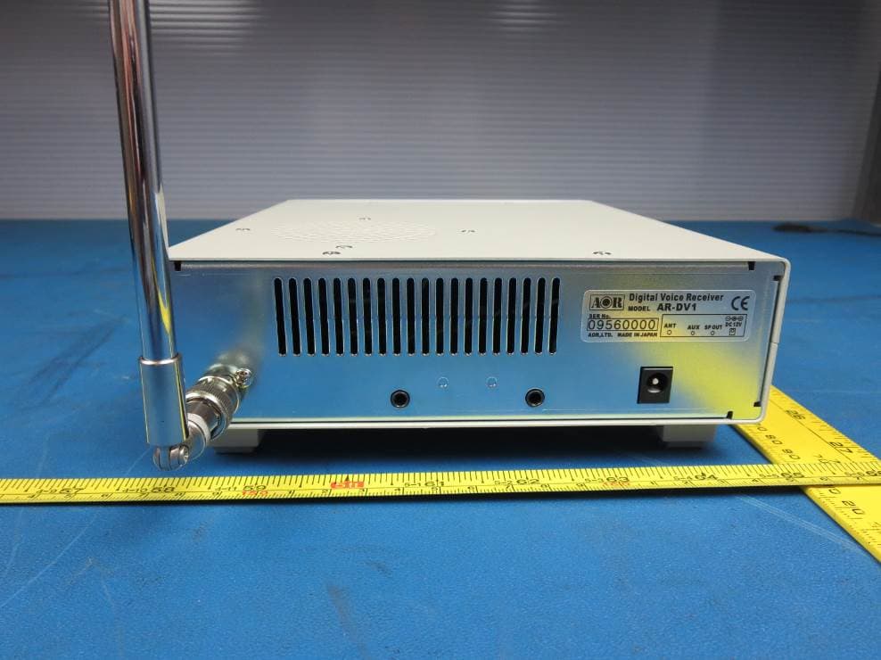
NVJARDV1
May 07, 2015Communications Receiver
Equipment Class
CSR - Scanning Receiver
NVJAR5001D
Aug 21, 2012Digital Processing Communication Receiver
Equipment Class
CSR - Scanning Receiver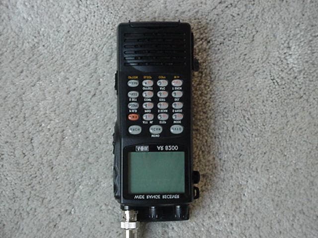
NVJAR8200MK3B
Oct 30, 2002Wide Band Scanning Receiver
Equipment Class
CSR - Scanning Receiver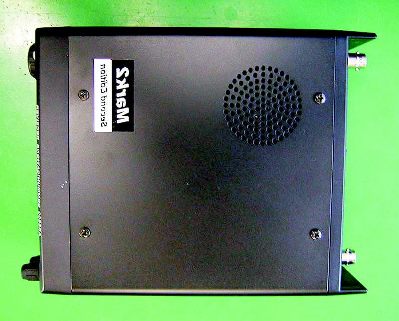
NVJAR8600MK2B
Jul 14, 2002Transportable wide band all mode receiver
Equipment Class
CSR - Scanning Receiver