NVJAR5001DDigital Processing Communication Receiver
AOR USA Inc.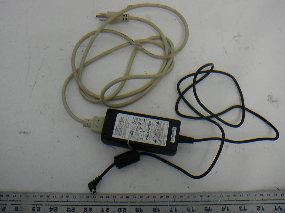
Click to zoom
Application Details
- Equipment Class
- CSR - Scanning Receiver
- Date of Grant
- Aug 21, 2012
- Application Purpose
- Original Equipment
- Date of Application
- Aug 17, 2012
- Equipment Note
- Digital Processing Communication Receiver
- Frequency Range
- 894.00000000 - 960.00000000
- Company
- AOR USA Inc.
- Country
- United States
Documents & Files
Document Text
Text extracted from the exhibit documents filed with the FCC. Open a document above to read the original.
Users Manual
® AR5001D Digital Processing Communications Receiver Operating manual AOR, LTD. 1 Table of Contents 1 INTRODUCTION ..................................................................................................................................... 5 1-1 INTRODUCTION .............................................................................................................................. 5 1-2 TAKE CARE OF YOUR RECEIVER ................................................................................................ 7 1-3 INCLUDED IN THIS PACKAGE ....................................................................................................... 8 2 CONTROLS AND FUNCTIONS ........................................................................................................... 12 2-1 FRONT PANEL ............................................................................................................................... 12 2-2 REAR PANEL ................................................................................................................................. 13 2-3 LCD DISPLAY ................................................................................................................................ 14 2-4 KEYPAD ......................................................................................................................................... 15 2-4-1 FRONT PANEL KEYS ............................................................................................................. 15 3 GETTING STARTED............................................................................................................................ 21 3-1 MAKING THE AR5001D READY FOR OPERATION .................................................................... 21 3-1-1 CONNECT THE ANTENNA ..................................................................................................... 21 3-1-2 CONNECT POWER ................................................................................................................ 21 3-2 SWITCHING ON FOR THE FIRST TIME ...................................................................................... 21 3-3 VOLUME CONTROL ...................................................................................................................... 22 3-4 SQUELCH CONTROL ................................................................................................................... 23 3-5 VFO SELECTION ........................................................................................................................... 23 3-5-1 TUNING FREQUENCY ........................................................................................................... 24 3-6 RECEIVE MODE ............................................................................................................................ 25 3-6-1 AUTO MODE SELECTION ...................................................................................................... 26 3-6-2 RECEIVE MODE SELECTION ............................................................................................... 27 3-7 CHANGING THE FREQUENCY STEP.......................................................................................... 27 3-8 IF BANDWIDTH ............................................................................................................................. 28 3-8-1 MANUALLY SELECTING IF BANDWIDTH ............................................................................. 29 4 ADDITIONAL SETTINGS ..................................................................................................................... 30 4-1 AGC (AUTOMATIC GAIN CONTROL) ........................................................................................... 30 4-2 ATTENUATOR / RF AMPLIFIER .................................................................................................... 30 4-3 RF GAIN ......................................................................................................................................... 31 4-4 ANTENNA INPUT ........................................................................................................................... 31 4-5 KEYLOCK ....................................................................................................................................... 32 5 ADVANCED FUNCTIONS .................................................................................................................... 32 5-1 SPECTRUM DISPLAY ................................................................................................................... 32 5-1-1 ACTIVATING THE SPECTRUM DISPLAY .............................................................................. 33 5-1-2 CHANGING THE FREQUENCY SPAN ................................................................................... 33 2 5-1-3 MOVING THE SPECTRUM ..................................................................................................... 33 5-1-4 CHANGING THE MARKER FREQUENCY ............................................................................. 33 5-1-5 DEACTIVATING THE SPECTRUM DISPLAY ......................................................................... 33 5-2 MULTI CHANNEL RECEIVE .......................................................................................................... 33 5-2-1 DUAL CHANNEL RECEIVE IN OFFSET MODE .................................................................... 33 5-2-2 DUAL BAND RECEIVE ........................................................................................................... 35 5-2-3 TRIPLE CHANNEL RECEIVE ................................................................................................. 36 5-3 MANAGING A SD CARD ............................................................................................................... 36 5-3-1 FORMAT A SD CARD .............................................…
Text truncated - open the document above for the full version.
Attestation Statements
AOR U.S.A., INC. 20655 S. Western Ave. Phone: 310-787-8615 Suite 112 Fax: 310-787-8619 Torrance, CA 90501 URL: www.aorusa.com Email: [email protected] Statements of Compatibility with FCC Rules – part 15.121 FCC ID: NVJAR5001D This scanning receiver cannot be used or modified to receive cellular radiotelephony frequencies. This is achieved by the key features described in detailed statements below. 1. Statement assessing the vulnerability of AOR receiver model AR5001D to possible modifications and describing design steps taken to make the tuning, control and filtering circuitry inaccessible (15.121 (a)): The receiver portion of the equipment under this application scans the frequency bands 40 kHz to 823.990 MHz, 849.010 to 868.990 MHz and 894.010 to 3150 MHz. The receiver circuitry cannot be altered to enable it to scan the cellular bands by means of clipping the leads of components, installing a diode and/or jumper wire, or by any other such simple modification. Nor can the receiver be made to scan the cellular bands by replacing a plug-in semiconductor chip, because no such plug-in chips are utilized anywhere in the receiver. The semiconductor chips that are utilized in the tuning function of the equipment cannot be reprogrammed. The tuning, control and filtering circuitry of the receiver is controlled by a microprocessor firmware, which is unalterable by the user (and it is also unalterable by the manufacturer’s own support and distribution staff, and their resellers). Any attempt to modify the circuitry cannot therefore result in achieving access to the cellular bands, but is likely to make the receiver inoperable. 2. Statement relating to cellular band rejection (15.121 (b)): The FCC requirement stipulates that scanning receivers shall reject any signals from the cellular radiotelephone service frequency bands that are 38dB or lower (at 12 dB SINAD). The construction of the equipment under this application is such that image rejection is typically 50 dB, therefore with a more than sufficient margin for adequate suppression of any image frequencies related to the cellular radiotelephone signals. This aspect was tested by the receiver placed in a scanning mode, and a full scan was performed for each of the following 6 test frequencies: 824, 836, 849, 869, 880, 894 MHz. There were no spurious responses detected within the entire frequency range of the receiver with a rejection ratio more than 38 dB. In view of the above, the equipment complies with parts 15.121 of the FCC rules.
External Photos
AOR USA, INC. FCC ID: NVJAR5001D Report Number: R1207099 Page 38 of 42 FCC Part 15B Test Report 9 Exhibit C- EUT Photos 9.1 EUT Front View 9.2 EUT Rear View AOR USA, INC. FCC ID: NVJAR5001D Report Number: R1207099 Page 39 of 42 FCC Part 15B Test Report 9.3 EUT Side View 9.4 EUT – AC/DC Power Supply View
ID Label/Location Info
AOR USA, INC. FCC ID: NVJAR5001D Report Number: R1207099 Page 33 of 42 FCC Part 15B Test Report 7 Exhibit A – FCC Equipment Labeling Requirements 7.1 FCC ID Label Requirements As per FCC §2.925, (a) Each equipment covered in an application for equipment authorization shall bear a nameplate or label listing the following: (1) FCC Identifier consisting of the two elements in the exact order specified in §2.926. The FCC Identifier shall be preceded by the term FCC ID in capital letters on a single line, and shall be of a type size large enough to be legible without the aid of magnification. Example: FCC ID: XXX123 Where: XXX—Grantee Code, 123—Equipment Product Code As per FCC §15.19, (3) All other devices shall bear the following statement in a conspicuous location on the device: This device complies with part 15 of the FCC Rules. Operation is subject to the following two conditions: (1) This device may not cause harmful interference, and (2) This device must accept any interference received, including interference that may cause undesired operation. (4) The label shall not be a stick-on, paper label. The label on these products shall be permanently affixed to the product and shall be readily visible to the purchaser at the time of purchase, as described in §2.925(d) of this chapter. “Permanently affixed” means that the label is etched, engraved, stamped, silk screened, indelibly printed, or otherwise permanently marked on a permanently attached part of the equipment or on a nameplate of metal, plastic, or other material fastened to the equipment by welding, riveting, or a permanent adhesive. The label must be designed to last the expected lifetime of the equipment in the environment in which the equipment may be operated and must not be readily detachable. As per FCC §15.121(f) (f) Scanning receivers shall have a label permanently affixed to the product, and this label shall be readily visible to the purchaser at the time of purchase. The label shall read as follows: WARNING: MODIFICATION OF THIS DEVICE TO RECEIVE CELLULAR RADIOTELEPHONE SERVICE SIGNALS IS PROHIBITED UNDER FCC RULES AND FEDERAL LAW. AOR USA, INC. FCC ID: NVJAR5001D Report Number: R1207099 Page 34 of 42 FCC Part 15B Test Report 7.2 FCC ID Label Contents and Location
Test Report
Note: This test report is prepared for the customer shown above and for the device described herein. It may not be duplicated or used in part without prior written consent from Bay Area Compliance Laboratories Corp. This report must not be used by the customer to claim product certification, approval, or endorsement by A2LA* or any agency of the Federal Government. * This report may contain data that are not covered by the A2LA accreditation and are marked with an asterisk “*” (Rev.3) FCC PART 15B TEST AND MEASUREMENT REPORT For AOR USA, INC. 20655 S. Western Ave., Suite 112, Torrance, CA 90501, USA FCC ID: NVJAR5001D Model: AR5001D Report Type: Original Report Product Type: Digital Processing Communications Receiver Prepared By: Charles Vergonio Report Number: R1207099 Report Date: 2012-08-01 Reviewed By: Victor Zhang EMC/RF Lead Bay Area Compliance Laboratories Corp. 1274 Anvilwood Avenue, Sunnyvale, CA 94089, USA Tel: (408) 732-9162 Fax: (408) 732 9164 AOR USA, INC. FCC ID: NVJAR5001D Report Number: R1207099 Page 2 of 42 FCC Part 15B Test Report TABLE OF CONTENTS 1 GENERAL INFORMATION ............................................................................................................................... 5 1.1 PRODUCT DESCRIPTION FOR EQUIPMENT UNDER TEST (EUT)........................................................................... 5 1.2 MECHANICAL DESCRIPTION OF EUT ................................................................................................................. 5 1.3 OBJECTIVE......................................................................................................................................................... 5 1.4 RELATED SUBMITTAL(S)/GRANT(S)................................................................................................................... 5 1.5 TEST METHODOLOGY........................................................................................................................................ 5 1.6 MEASUREMENT UNCERTAINTY.......................................................................................................................... 6 1.7 TEST FACILITY................................................................................................................................................... 6 2 SYSTEM TEST CONFIGURATION .................................................................................................................. 7 2.1 JUSTIFICATION................................................................................................................................................... 7 2.2 EUT EXERCISE SOFTWARE................................................................................................................................7 2.3 EQUIPMENT MODIFICATIONS............................................................................................................................. 7 2.4 LOCAL SUPPORT EQUIPMENT............................................................................................................................. 7 2.5 EUT INTERNAL CONFIGURATION DETAILS........................................................................................................ 7 2.6 EXTERNAL I/O CABLING LIST AND DETAILS..................................................................................................... 7 2.7 POWER SUPPLY LIST AND DETAILS.................................................................................................................... 7 3 SUMMARY OF TEST RESULTS........................................................................................................................ 8 4 FCC §15.107 – AC LINE CONDUCTED EMISSIONS ..................................................................................... 9 4.1 APPLICABLE STANDARDS.................................................................................................................................. 9 4.2 EUT SETUP........................................................................................................................................................ 9 4.3 TEST SETUP BLOCK DIAGRAM......................................................................................................................... 10 4.4 TEST PROCEDURE............................................................................................................................................ 10 4.5 CORRECTED AMPLITUDE & MARGIN CALCULATION....................................................................................... 10 4.6 TEST EQUIPMENT LIST AND DETAILS.............................................................................................................. 11 4.7 TEST ENVIRONMENTAL CONDITIONS............................................................................................................... 11 4.8 SUMMARY OF TEST RESULTS........................................................................................................................... 11 4.9 CONDUCTED EMISSIONS TEST PLOTS AND DATA............................................................................................. 12 5 FCC §15.109 – RADIATED EMISSIONS ......................................................................................................... 14 5.1 APPLICABLE STANDARD.................................................................................................................................. 14 5.2 TEST SETUP..................................................................................................................................................... 14 5.3 TEST SETUP BLOCK DIAGRAM......................................................................................................................... 15 5.4 TEST PROCEDURE............................................................................................................................................ 16 5.5 CORRECTED AMPLITUDE & MARGIN CALC…
Text truncated - open the document above for the full version.
Test Setup Photos
AOR USA, INC. FCC ID: NVJAR5001D Report Number: R1207099 Page 35 of 42 FCC Part 15B Test Report 8 Exhibit B- Test Setup Photos 8.1 AC Line Conducted Emissions – Front View 8.2 AC Line Conducted Emissions – Side View AOR USA, INC. FCC ID: NVJAR5001D Report Number: R1207099 Page 36 of 42 FCC Part 15B Test Report 8.3 Radiated Spurious Emissions below 1 GHz – Front View 8.4 Radiated Spurious Emissions below 1GHz – Back View AOR USA, INC. FCC ID: NVJAR5001D Report Number: R1207099 Page 37 of 42 FCC Part 15B Test Report 8.5 Radiated Spurious Emissions above 1 GHz – Front View 8.6 Radiated Spurious Emissions above 1 GHz– Rear View
Contact Information
Applicant
Shigeru Takano
Test Firm
Bay Area Compliance LaboratoryJohn Chan
Technical Specifications
| # | Rule Parts | Frequency Range | Power Output |
|---|---|---|---|
| 3 | 15B | 894 MHz - 960 MHz | - |
Other Applications from AOR USA Inc.
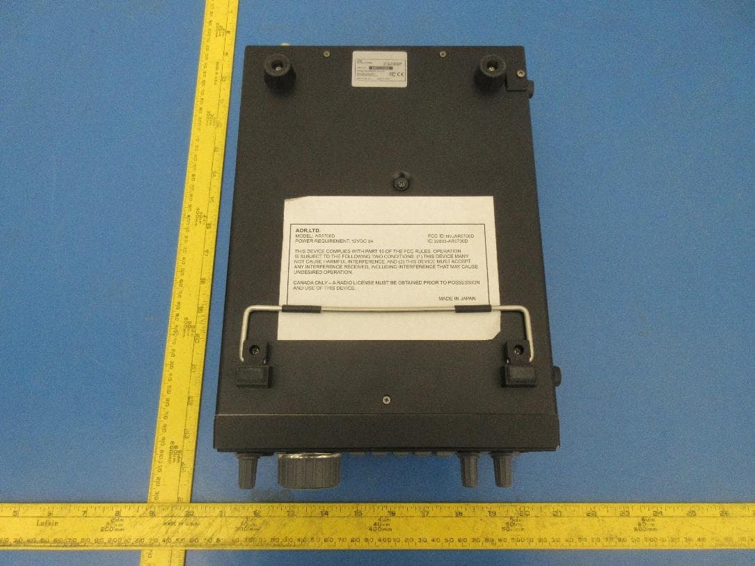
NVJAR5700D
Apr 21, 2020Digital Processing Communications Receiver
Equipment Class
CSR - Scanning Receiver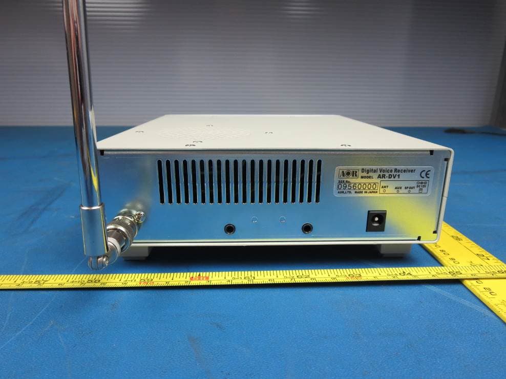
NVJARDV1
May 07, 2015Communications Receiver
Equipment Class
CSR - Scanning Receiver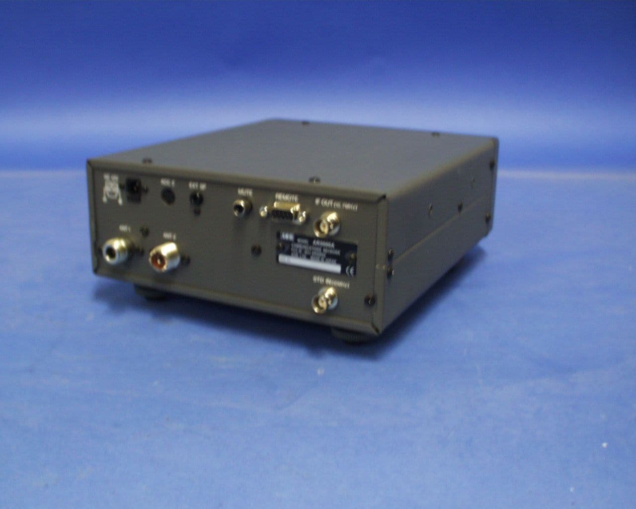
NVJAR5000A
May 31, 2004AR5000A+3B Communications Receiver
Equipment Class
CSR - Scanning Receiver
NVJAR8200MK3B
Oct 30, 2002Wide Band Scanning Receiver
Equipment Class
CSR - Scanning Receiver
NVJAR8600MK2B
Jul 14, 2002Transportable wide band all mode receiver
Equipment Class
CSR - Scanning Receiver