O3JNBS55XXBWIRELESS CDMA POINT-OF-SALE TERMINAL
NBS Payment Solutions - Division of NBS Technologies Inc.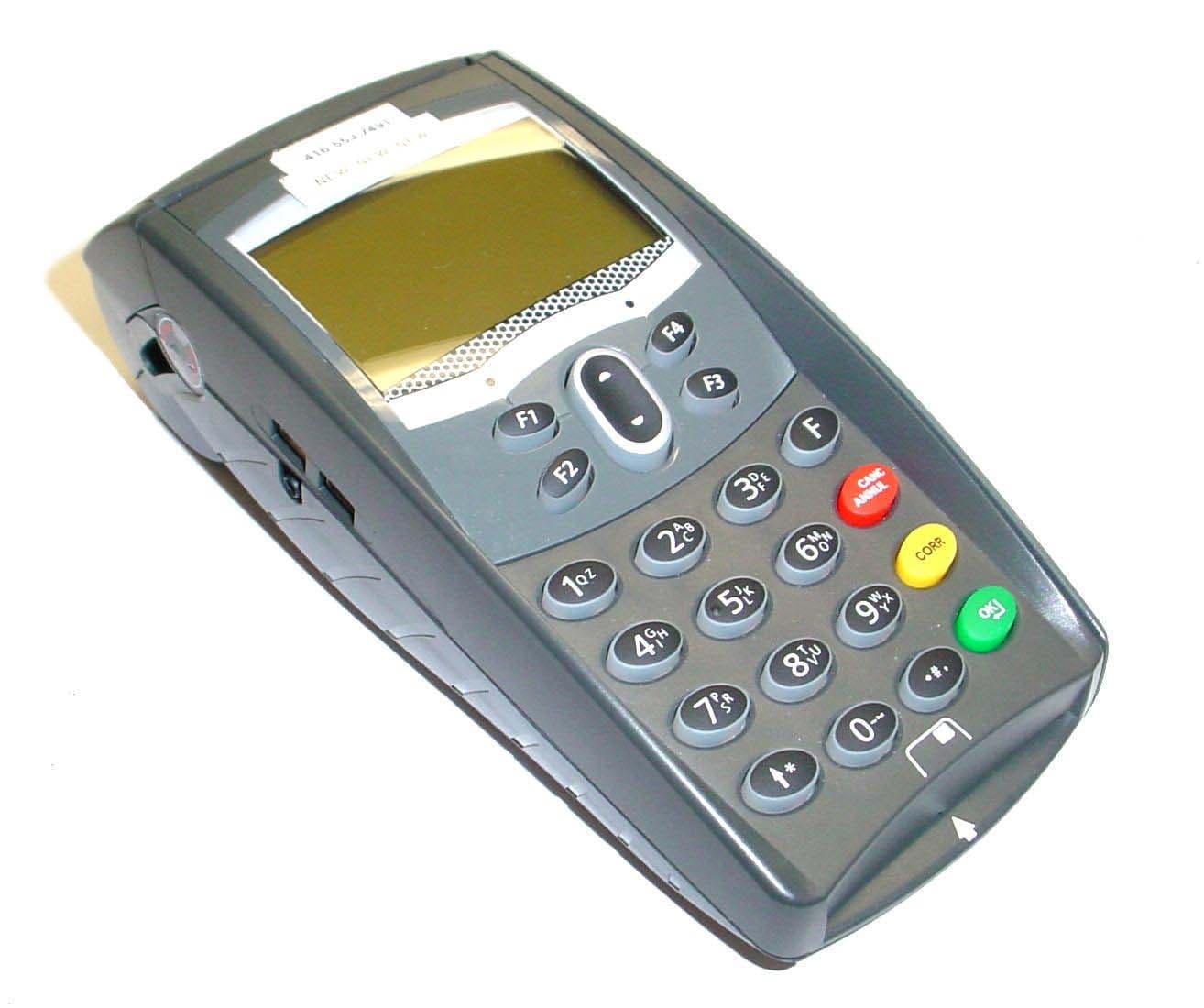
Click to zoom
Application Details
- Equipment Class
- PCB - PCS Licensed Transmitter
- Date of Grant
- Sep 06, 2007
- Application Purpose
- Original Equipment
- Date of Application
- Sep 06, 2007
- Equipment Note
- WIRELESS CDMA POINT-OF-SALE TERMINAL
- Frequency Range
- 1851.25000000 - 1908.75000000
- Country
- Canada
Documents & Files
Document Text
Text extracted from the exhibit documents filed with the FCC. Open a document above to read the original.
Users Manual
NBS5500™ TERMINAL INSTALLATION AND OPERATION MANUAL NBS5500 TERMINAL™ INSTALLATION & OPERATION MANUAL Copyright © May 17, 2005 NBS Technologies Inc. All rights reserved. Notice The content of this document is furnished for informational use only, is subject to change with out notice, and should not be construed as an assumption of liability by NBS Technologies Inc. NBS Technologies Inc. assumes no responsibility or liabil-ity for any inaccuracies that may appear in this document. NBS Technologies Inc. and the NBS Technologies Inc. logo are trademarks of NBS Technologies Inc. All other brand or product name s are the trademarks or regis- tered trademarks of their respective holders. NBS Part Number: DE-X5500-IOM-0A-F5TDCDMA ii NBS5500 INSTALLATION & OPERATION MANUAL 27 NOTES WWW.NBSTECH.COM 26 TRANSPORTING AND STORING THE NBS5500 • Use the original packing material for any unit transport or storage. • Disconnect the battery whenever the portable is not to be used for a period exceeding one month. The method to disconnect the battery is outlined in the "Changing the battery." ACCESSORIES USB TRAVEL ADAPTOR Connect the BA–USB travel adapter to the portable mini-USB slave connector to charge the battery. TABLE OF CONTENTS Product Regulatory Information ................................................4 Manufacturer’s Declaration of Co nformity ................................4 Introduction ...............................................................................7 Safety Instructions ....................................................................8 Characteristics of the NBS5500 ...............................................9 Unpacking the NBS5500 ........................................................10 Keypad Key Assignments .......................................................11 Daily Use ................................................................................11 Opening/Closing the Battery Cover Flap ................................13 De-Installing the SAM1 and SAM2 Modules ..........................14 Opening/Closing the CAM2 Cover Flap .................................14 De-Installing the SAM3 and SAM4 (o r SIM) Modules ............15 De-Installing the MMC or SDCARD ........................................16 The Secondary Smart Card Reader .......................................16 Installing the NBS5500 ...........................................................17 Installing the NBS5500 on its Base .....................................17 Connecting the Base Wires ..............................................17 Portable Connections .......................................................19 Connecting the Battery .....................................................19 Charging the Battery .........................................................20 Adjusting the Contrast .......................................................21 Installing a Roll of Paper .........................................................21 Maintaining a NBS5500 ..........................................................22 Operating the Portable in Case of Battery Failure ................22 Changing the Battery ........................................................22 The Lithium Battery ..........................................................23 Cleaning the NBS5500 .....................................................23 Transporting and Storing the NBS5500 ..................................24 Accessories ............................................................................24 iii WWW.NBSTECH.COM 4 PRODUCT REGULATORY INFORMATION Changes or modifications to this unit not expressly approved by NBS Technologies Inc. could void the user’s authority to oper- ate this equipment. MANUFACTURER’S DECLARATION OF CONFORMITY American Notice FCC Part 15 Compliance (EMC) This device complies with the re quirements in Part 15 of the FCC Rules for a Class A digital device. Operation is subject to the following two conditions: • This device may not cause harmful interference. • This device must accept any interference received, includ- ing interference that may cause undesired operation. Note : This equipment has been tested and found to comply with the limits for a Class A digital device, pursuant to Part 15 of the FCC Rules. These limits are designed to provide reason-able protection against harmful interference when the equip-ment is operated in a commerci al environment. This equipment generates, uses, and can radiate radio frequency energy and, if not installed and used in accordance with the instruction man-ual, may cause harmful interference to radio communications. Operation of this equipment in a residential area is likely to cause harmful interference in which case the user will be re- quired to correct the interference at his own expense. Warning : Changes or modifications not expressly approved by NBS technologies Inc. could void the user’s authority to oper-ate the equipment. NBS5500 INSTALLATION & OPERATION MANUAL 25 5. Carefully disconnect the bat- tery as follows: a) Unlock the connector by pressing the locking mechanism (See Arrow F1) while pulling wires (See Arrow F2), to disconnect the connector. Release the traction on it as soon as the connector comes unclipped. b) Finish extracting the connector by tilting it slightly (See Ar-row F3) to bring it away from the housing. 6. Connect and install the new battery following the instruc- tions in "Connecting the Battery." 7. Close the battery cover flap and charge the battery follow- ing the instructions in "Charging the Battery." 8. In order to preserve the en vironment, dispose of used bat- teries in compliance with current recycling legislation. THE LITHIUM BATTERY For the attention of maintenance departments: Warning : this equipment is provided with a lithium battery. There is a risk of explosion if th is battery is incorrectly replaced. Replace the battery with a battery recommended by the manu-facturer. • Dispose of used batteries ac co…
Text truncated - open the document above for the full version.
Cover Letter(s)
In reply to your recent questions: 1. FCC ID: The FCC Id of the device may not contain “wild cards”, such as XX, that stand for other alphanumeric characters. Please advise the applicant and let us know how they wish to proceed. Thanks. The XX in the FCC ID in NOT intended to be ‘wild cards’. The ‘wild cards’ comment in the Cover Letter was referring to the different models which will be introduced (if any) in the future pertaining to this filing. 2. LABEL LOCATION: Devices with non-routine label proposals - that is when placing a label inside the battery compartment: Applications for this type of label proposal must address the following items and must be provided in a cover letter (exhibit "label Location"); a. Provide justification such as limited space (e.g. the available label area on the device is limited because it is relatively small and has many contoured surfaces, keypads, LCD displays, charge contacts and/or other connectors....). b. How the FCC identifier or label will be readily viewable per FCC Rule 2.925 (d) (e.g. the batteries are designed for easy removal and the label will be visible whenever the batteries are removed for charging or replacement.....). c. How the FCC identifier or label will be readily viewable at the time of the purchase to comply with Part 2.925 (d) (e.g. the label will be readily visible at the time of purchase because the device will be marketed without the battery installed). NOTE: Devices utilizing a conventional battery and battery compartment not made for easy removal for charging or replacement may not have the label placed under the battery, and inside the battery compartment because this location is not visible from the outside of the equipment enclosure as required by Part 2.925 (d). See ID Label Location exhibit for justification. 3. Please provide a block diagram, parts list, and schematics for the Wavecom module. Wavecom has been contacted by applicant to submit the required exhibits to Timco. 4. Confidentiality: Please confirm whether this file “NBS55XXTXXX- B_OpDes_Wavecom.pdf” is to be held confidential. If so, please update the confidentiality request letter. This exhibit was obtained from the certified Wavecom Module (FCC ID: O9EQ2438F-M; Date of Grant: 06/06/2005) filing via FCC website. So, this exhibit is public and not confidential. 5. Test report “NBS55XXTXXX-B_TestRpt_EMC_NBS.pdf”: Section 6.7.5. The FCC allows the use of a RBW >= 1% of the 26dB emission bandwidth (10kHz is < 26dB EBW). Please revise plots or use a correction factor to integrate the power at the band- edges over the full bandwidth. See revised test report. 6. SAR: Please explain whether this device is CDMA2000. If so please provide the following information per FCC 3G policy: Yes, the device has a CDMA200 RTT1 capability. See the reply and the additional test result below. 7. SAR report section 11 test results: Please provide additional information per FCC’ s 3G and HSPA interim SAR procedures, as follows: a) CDMA MS Protocol Revision number. b) Applicability of test codes to simulate the required test conditions, as defined in 3GPP2, TIA, and other standards. c) Base station simulator and test device configuration info and procedures used to maximize output in all applicable modes, including code domain channels, power & relative gain levels. d) Identify CDMA Radio Configurations, Service Options, multiplex options, voice/data, code channel combinations and options used for the SAR tests. e) Because of the different RC's, SO's, data rates, channel combinations and modulations, filing should include justifications on the selection of applicable configurations to establish and maintain maximum output to demonstrate SAR compliance for other configurations that are not tested. In the test report, R&S CMD 80 was used to simulate CDMAOne (IS-95A and JSTD- 008) network with the following parameters and all SAR measurements were performed under this network. - MS P_Rev=1 for JSTD-008 & P_Rev=3 for IS-95A. - Test mode 1 - RC1/1, SO2, Traffic Channel @ 9600 bps. - All power bits were set all up for maximum output power. Since the device has CDMA2000 RTT1 capability, additional measurements have been performed as described below. Test equipment R&S Universal Radio Communication Tester (M/N: CMU200 1100.00008K02 S/N: 101911) Network Parameters MS P_Rev=6 All power bits up #1: Test Mode 1, RC1/1, SO55, MO1, Traffic Channel @ 9600 bps #2: Test Mode 3, RC3/3, SO55, MO1, FCH @ 9600 bps #3: Test Mode 3, RC3/3, SO32, MO1, FCH @ 9600 bps #4: Test Mode 3, RC3/3, SO32, MO1, FCH + SCH 0 @ 9600 bps - RF output power measurement result from the test report - Cellular Band: 824 – 849 MHz Transmitter Channel Output Fundamental Frequency (MHz) Measured Peak Conducted Power (dBm) * Calculated ERP (dBm) ERP Limit (dBm) Lowest 824.70 28.31 27.76 38.45 Middle 836.52 28.10 27.55 38.45 Highest 848.31 27.78 27.23 38.45 PCS Band: 1850 – 1910 MHz Transmitter Channel Output Fundamental Frequency (MHz) Measured Peak Conducted Power (dBm) *Calculated e.i.r.p. (dBm) e.i.r.p. Limit Lowest 1851.25 27.42 29.62 33.0 Middle 1880.00 27.92 30.12 33.0 Highest 1908.75 27.00 29.20 33.0 - Additional RF output power measurement result for CDMA2000 - CDMA2000 Cellular Test Mode Radio Configuration Channel Frequency (MHz) Conducted Peak Power (dBm) 1013 824.70 27.59 0384 836.52 27.50 #1 1 RC1/1, SO55 0777 848.31 27.27 1013 824.70 27.56 0384 836.52 27.41 #2 RC3/3, SO55, FCH @9600 bps 0777 848.31 27.24 1013 824.70 27.53 0384 836.52 27.40 #3 RC3/3, SO32, FCH @9600 bps 0777 848.31 27.24 1013 824.70 27.53 0384 836.52 27.39 #4 3 RC3/3, SO32, FCH + SCH 0 @9600 bps 0777 848.31 27.24 CDMA2000 PCS Test Mode Radio Configuration Channel Frequency (MHz) Conducted Peak Power (dBm) 0025 1851.25 26.96 0600 1880.00 27.57 #1 1 RC1/1, SO55 1175 1908.75 26.35 0025 1851.25 26.97 0600 1880.00 27.59 #2 RC3/3, SO55, FCH @9600 bps 1175 1908.75 26.44 0025 1851.25 26.91 0600 1880.00 27.51 #3 RC3/3, SO32, FCH @9600 bps 1175 1908.75 26.36 00…
Text truncated - open the document above for the full version.
Cover Letter(s)
June 26, 2007 FEDERAL COMMUNICATIONS COMMISSION 7435 Oakland Mills Road Columbia, MD 21046 U.S.A. Subject: Authority to Act as an Agent to FCC Applicant: NBS Technologies Inc. Product: NBS55XX Model: NBS55XXTXXX-B FCC ID: O3JNBS55XXB Dear Sir/Madam, I hereby appoint UltraTech Engineering Labs Inc. (UltraTech) to act as my agent in preparation of this application to F.C.C. for authorization of equipment under F.C.C. Rules. I also certify that the information provided, properly described the device or system for which authorization is required. Regards, Dragoslav Jovanovic Manager Hardware Development NBS Technologies Inc.
Cover Letter(s)
July 17, 2007 Federal Communications Commission Authorization and Evaluation Division Confidentiality Request regarding application for certification of FCC ID: O3JNBS55XXB. Pursuant to Sections 0.457 and 0.459 of the Commission’s Rules, we hereby request confidential treatment of information accompanying this application as outlined below: Exhibit Type File Name Block Diagram NBS55XXTXXX-B_BlkDia_NBS.pdf Operational Description NBS55XXTXXX-B_OpDes_NBS.pdf Parts List NBS55XXTXXX-B_PartsLst_NBS_1.pdf Parts List NBS55XXTXXX-B_PartsLst_NBS_2.pdf Schematics NBS55XXTXXX-B_Schem_NBS.pdf The above materials contain trade secrets and proprietary information not customarily released to the public. The public disclosure of these materials may be harmful to the applicant and provide unjustified benefits to its competitors. The applicant understands that pursuant to Section 0.457 of the Rules, disclosure of this application and all accompanying documentation will not be made before the date of the Grant for this application. Sincerely, Dragoslav Jovanovic Manager Hardware Development NBS Technologies Inc.
Cover Letter(s)
July 30, 2007 Timco Engineering, Inc. 849 NW State Road 45 P.O. Box 370 Newberry, Florida 32669 Subject: O3JNBS55XXB - Label Location 1. The available label area on the device is limited because it is small and has many contoured surfaces, keypad, LCD display, printer, card readers, sockets, charge contacts and other connectors. 2. Battery pack is designed for easy removal and the label will be visible whenever the batteries are removed. Even when the battery is not completely removed from the device the label is visible. 3. The label will be readily visible at the time of purchase because the device will be delivered without the battery installed. Sincerely, Dragoslav Jovanovic Manager Hardware Development NBS Technologies Inc. T: 1.416.621.1911 F: 1.416..621.8875 E: [email protected]
Cover Letter(s)
July 11, 2007 TIMCO ENGINEERING INC. P.O. Box 370 849 N.W. State Road 45 Newberry, Florida Subject: FCC Equipment Certification Application under FCC 47 CFR, Parts 2, 22 (Subpart H) and 24 (Subpart E) – Non-broadcast Radio Transceivers Operating in the Frequency Bands 824.7 – 848.31 MHz and 1850.25 – 1908.75 MHz Applicant: NBS Technologies Inc. Product: NBS55XX Model: NBS55XXTXXX-B FCC ID: O3JNBS55XXB Dear Sir/Madam, As appointed agent for NBS Technologies Inc., we submit the application for certification of the above product. Please review all files uploaded to TIMCO Web Site. The NBS Technologies POS terminal, Model NBS55XXTXXX-B, incorporates a certified Wavecom Module (FCC ID: O9EQ2438F-M; Date of Grant: 06/06/2005). The incorporated radio is identical in design and construction to the original. Since, there is no change on the radio module’s operation, the following tests are performed to ensure the continuing compliance with different enclosure and power supply conditions: (1) RF output (2) Occupied Bandwidth (3) Transmitter spurious/harmonic conducted and radiated emissions. (4) RF exposure evaluation for portable application (SAR). For all other required tests pertaining to FCC Parts 2, 22 and 24, refer to the radio module original filing test report from Wavecom, submitted with this application via Timco E-filling site. Notes: • All confidential items associating to Wavecom Radio Module will be submitted along with this application directly by Wavecom . • The digital circuit portion of the POS Terminal has been tested and found to comply with FCC Part 15, Subpart B, Class A Digital Devices. Ultratech can provide the engineering test report upon request. • The model appearing on the terminal may be displayed using numbers (in place of “X”) instead of “XXTXXX-B”, see ID label exhibit for model number explanation. These designations indicate the different features for marketing purposes and clarification of the device. The electronics are equivalent regardless of these designations. If you have any queries, please do not hesitate to contact us. Yours truly, Tri Minh Luu, P. Eng., V.P., Engineering TML/DH UltraTech Group of Labs Ultratech’s Accreditations: 0685 31040/SIT C-1376 46390-2049 200093-0 SL2-IN-E-1119R 3000 Bristol Circle, Oakville, Ontario, Canada L6H 6G4 Tel.: (905) 829-1570 Fax.: (905) 829-8050 Website: www.ultratech-labs.com Email: [email protected]
ID Label/Location Info
1 May 16, 2007 Product Name: NBS55XX Model: NBS55XXTXXX-B Terminal Label NBS S/N: TDXXXXXX NBS55XX Model: NBS55XXTXXX-B ||||||||||||||||||||||||||||||||||||||||||||||||||||||||| ||||||||||||||||||||||||||||||||||||||||||||||||||||||||| CDMA Radio S/N: YXXYZZZZ ||||||||||||||||||||||||||||||||||||||||||||||||||||||||| XXXXXXXXX ||||||||||||||||||||||||||||||||||||||||||||||||||||||||| XXXXXYYZZZZZZZZ Made in/Fait au: France MFD: XX/XXXX FCC ID: O3JNBS55XXB IC: 2279B - NBS55XXB H/W: ICL Y Model number explanation NBS 5 5 XX T XXX-B Brand Name Configuration: 001 = Black, TD Bank logo Product Family 002 = Black, No logo 003 = Communication Type Device Type: 0 = No Radio A = Accessories 5 = CDMA Radio B = Base 6 = GPRS Radio K = Kit 7 = Bluetooth Radio P = PINpad 8 = Wi-Fi Radio T = Terminal Hardware variations: 00 = Basic (MSR, Smart Card, MMC, SAM, USB) 2 Terminal Label location Terminal label with FCC and IC ID
Parts List/Tune Up Info
June 26, 2007 UltraTech Engineering Labs Inc. 3000 Bristol Circle Oakville, Ontario, L6H 6G4 Canada Subject: Tune-up procedure Applicant: NBS Technologies Inc. Product: NBS55XX Model: NBS55XXTXXX-B Dear Sir/Madam, I certify that this device does not have a tuning procedure; the RF output power and channel frequencies are programmed in the Q2438 RF module firmware by Wavecom. Regards, Dragoslav Jovanovic Manager Hardware Development NBS Technologies Inc.
Test Report
NBS55XX Model No.: NBS55XXTXXX-B FCC ID: O3JNBS55XXB Applicant: NBS Technologies Inc. 703 Evans Avenue, Suite 400 Toronto, Ontario Canada M9C 5E9 Tested in Accordance With Federal Communications Commission (FCC) 47 CFR, PARTS 2, 22 (Subpart H) and 24 (Subpart E) UltraTech's File No.: MIS-061FCC22H24E This Test report is Issued under the Authority of Tri M. Luu, Professional Engineer, Vice President of Engineering UltraTech Group of Labs Date: July 31, 2007 Report Prepared by: Dan Huynh Issued Date: July 31, 2007 Tested by: Wayne Wu, RFI/EMI Technician Test Dates: May 17 - June 12 & July 31, 2007 The results in this Test Report apply only to the sample(s) tested, and the sample tested is randomly selected. This report must not be used by the client to claim product endorsement by NVLAP or any agency of the US Government. UltraTech 3000 Bristol Circle, Oakville, Ontario, Canada, L6H 6G4 Tel.: (905) 829-1570 Fax.: (905) 829-8050 Website: www.ultratech-labs.com , Email: [email protected], Email: [email protected] 0685 31040/SIT C-1376 46390-2049 200093-0 SL2-IN-E-1119R FCC Parts 2 & 22(H) and 24(E) Contents i NBS55XX, Model NBS55XXTXXX-B FCC ID: O3JNBS55XXB ULTRATECH GROUP OF LABS File #: MIS-061FCC22H24E 3000 Bristol Circle, Oakville, Ontario, Canada L6H 6G4 July 31, 2007 Tel. #: 905-829-1570, Fax. #: 905-829-8050, Email: [email protected], Website: http://www.ultratech-labs.com All test results contained in this engineering test report are traceable to National Institute of Standards and Technology (NIST) TABLE OF CONTENTS EXHIBIT 1. SUBMITTAL CHECK LIST ..........................................................................................................................................1 EXHIBIT 2. INTRODUCTION ............................................................................................................................................................2 2.1. SCOPE ............................................................................................................................................................................................2 2.2. RELATED SUBMITTAL(S)/GRANT(S).......................................................................................................................................2 2.3. NORMATIVE REFERENCES .......................................................................................................................................................2 EXHIBIT 3. PERFORMANCE ASSESSMENT .................................................................................................................................3 3.1. CLIENT INFORMATION ..............................................................................................................................................................3 3.2. EQUIPMENT UNDER TEST (EUT) INFORMATION.................................................................................................................3 3.3. EUT’S TECHNICAL SPECIFICATIONS......................................................................................................................................4 3.4. LIST OF EUT’S PORTS.................................................................................................................................................................4 3.5. ANCILLARY EQUIPMENT ..........................................................................................................................................................4 EXHIBIT 4. EUT OPERATING CONDITIONS AND CONFIGURATIONS DURING TESTS...................................................5 4.1. CLIMATE TEST CONDITIONS ...................................................................................................................................................5 4.2. OPERATIONAL TEST CONDITIONS & ARRANGEMENT FOR TEST SIGNALS.................................................................5 EXHIBIT 5. SUMMARY OF TEST RESULTS..................................................................................................................................6 5.1. LOCATION OF TESTS..................................................................................................................................................................6 5.2. APPLICABILITY & SUMMARY OF EMISSION TEST RESULTS............................................................................................6 5.3. MODIFICATIONS INCORPORATED IN THE EUT FOR COMPLIANCE PURPOSES............................................................6 5.4. DEVIATION OF STANDARD TEST PROCEDURES .................................................................................................................6 EXHIBIT 6. MEASUREMENTS, EXAMINATIONS & TEST DATA FOR EMC EMISSIONS ..................................................7 6.1. TEST PROCEDURES ....................................................................................................................................................................7 6.2. MEASUREMENT UNCERTAINTIES ..........................................................................................................................................7 6.3. MEASUREMENT EQUIPMENT USED .......................................................................................................................................7 6.4. ESSENTIAL/PRIMARY FUNCTIONS AS DECLARED BY THE MANUFACTURER ............................................................7 6.5. RF POWER OUTPUT [§§ 2.1046 & 22.913 & 24.232] .................................................................................................................8 6.6. OCCUPIED BANDWIDTH [§ 2.1049] ........................................................................................................................................ 10 6.7. SPURIOUS EMISSIONS AT ANTENNA TERMINALS [§§ 2.1051 22.917 & 24.238]............................................................. 17 6.8. FIELD STRENGT…
Text truncated - open the document above for the full version.
Test Report
NBS5500 Model No.: NBS55XXTXXX-B Tested For NBS Technologies Inc. 703 Evans Avenue, Suite 400 Toronto, ON Canada, M9C 5E9 In Accordance With SAR (Specific Absorption Rate) Requirements using guidelines established in IEEE Standard C95.1, FCC OET Bulletin 65 (Supplement C), Industry Canada RSS-102(Issue 2), EN 50360 (Council Recommendation 1999/519/EC) and ACA 2003 / ARPANSA Standard UltraTech's File No.: MIS-061-SAR This Test report is Issued under the Authority of Tri M. Luu, Professional Engineer, Vice President of Engineering UltraTech Group of Labs Date: July 20, 2007 Report Prepared by: JaeWook Choi Tested by: Carolyn Luu Issued Date: July 20, 2007 Test Dates: June 04, 05, 06 & 07, 2007 The results in this Test Report apply only to the sample(s) tested, which has been randomly selected. UltraTech 3000 Bristol Circle, Oakville, Ontario, Canada, L6H 6G4 Telephone (905) 829-1570 Facsimile (905) 829-8050 Website: www.ultratech-labs.com Email: [email protected] SPECIFIC ABSORPTION RATE (SAR) Page 1 IEEE Standard C95.1, FCC OET Bulletin 65 (Supplement C), Industry Canada RSS-102 (Issue 2) and ACA Radiocommunications (Electromagnetic Radiation – Human Exposure) Amendment Standard 2000 (No. 1) NBS5500 M/N: NBS55XXTXXX-B FCC ID: O3J-NBS55XXB ULTRATECH GROUP OF LABS File #: MIS-061-SAR 3000 Bristol Circle, Oakville, Ontario, Canada L6H 6G4 July 20, 2007 Tel. #: 905-829-1570, Fax. #: 905-829-8050, Email: [email protected], Website: http://www.ultratech-labs.com • Assessed by ITI (UK) Competent Body, NVLAP (USA) Accreditation Body & ACA/AUSTEL (Australia), VCCI (Japan) • Accredited by Industry Canada (Canada) under ACC-LAB (Europe/Canada MRA and APEC/Canada MRA) • Recognized/Listed by FCC (USA ) • All test results contained in this engineering test report are traceable to National Institute of Standards and Technology (NIST) TABLE OF CONTENTS EXHIBIT 1. INTRODUCTION ................................................................................................................................................ 5 1.1. SCOPE ............................................................................................................................................................................... 5 1.2. REFERENCES................................................................................................................................................................... 5 EXHIBIT 2. PERFORMANCE ASSESSMENT ..................................................................................................................... 6 2.1. CLIENT AND MANUFACTURER INFORMATION ...................................................................................................... 6 2.2. DEVICE UNDER TEST (D.U.T.) DESCRIPTION.............................................................................................................. 6 2.3. LIST OF D.U.T.’S ACCESSORIES:.................................................................................................................................. 7 2.4. SPECIAL CHANGES ON THE D.U.T.’S HARDWARE/SOFTWARE FOR TESTING PURPOSES ............................. 7 2.5. ANCILLARY EQUIPMENT ............................................................................................................................................. 7 2.6. GENERAL TEST CONFIGURATIONS ........................................................................................................................... 7 2.6.1. Equipment Configuration ........................................................................................................................................... 7 2.6.2. Exercising Equipment................................................................................................................................................. 7 2.7. SPECIFIC OPERATING CONDITIONS...................................................................................................................................... 7 2.8. BLOCK DIAGRAM OF TEST SETUP ............................................................................................................................. 8 EXHIBIT 3. SUMMARY OF TEST RESULTS ...................................................................................................................... 9 3.1. LOCATION OF TESTS ..................................................................................................................................................... 9 3.2. APPLICABILITY & SUMMARY OF SAR RESULTS..................................................................................................... 9 EXHIBIT 4. MEASUREMENTS, EXAMINATIONS & TEST DATA .............................................................................. 10 4.1. TEST SETUP ................................................................................................................................................................... 10 4.2. PHOTOGRAPH OF D.U.T. AND ALL ACCESORIES................................................................................................................ 11 4.3. PHOTOGRAPHS OF D.U.T. POSITION ........................................................................................................................13 4.3.1. Body Configuration .................................................................................................................................................. 13 4.3.1.1. Right side of DUT in parallel to the phantom with spacing of 10 mm..................................................................................... 13 4.3.1.2. Left side of DUT in parallel to the phantom with…
Text truncated - open the document above for the full version.
Contact Information
Applicant
Dragoslav Jovanovic(Manager, Engineering)
Test Firm
UltraTech Engineering Labs Inc.Tri Luu
Technical Specifications
| # | Rule Parts | Frequency Range | Power Output | Emission | Tolerance |
|---|---|---|---|---|---|
| 2 | 24E | 1.85 GHz - 1.91 GHz | 1.028 W | 1M29F9W | 2.5 ppm |
Other Applications from NBS Payment Solutions - Division of NBS Technologies Inc.
O3JNBS1200
Jan 27, 2008NBS1200
Equipment Class
DXT - Part 15 Low Power Transceiver, Rx Verified
O3JNBS5030
Dec 20, 2007WIRELESS POS TERMINAL BASE
Equipment Class
DSS - Part 15 Spread Spectrum Transmitter
O3JNBS5700
Dec 20, 2007wireless pos terminal
Equipment Class
DSS - Part 15 Spread Spectrum Transmitter
O3JNBS56XXT
Mar 16, 2006WIRELESS GSM/GPRS POINT-OF-SALE TERMINAL
Equipment Class
PCT - PCS Licensed Transmitter worn on body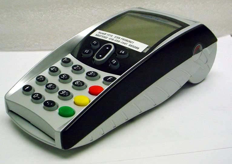
O3JNBS55XXT
May 26, 2005Wireless CDMA Point-of-Sale Terminal
Equipment Class
PCT - PCS Licensed Transmitter worn on body