O3JNBS55XXTWireless CDMA Point-of-Sale Terminal
NBS Payment Solutions - Division of NBS Technologies Inc.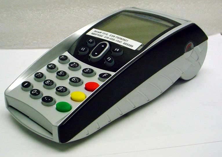
Click to zoom
Application Details
- Equipment Class
- PCT - PCS Licensed Transmitter worn on body
- Date of Grant
- May 26, 2005
- Application Purpose
- Original Equipment
- Date of Application
- May 26, 2005
- Equipment Note
- Wireless CDMA Point-of-Sale Terminal
- Frequency Range
- 824.70000000 - 848.31000000
- Country
- Canada
Documents & Files
Document Text
Text extracted from the exhibit documents filed with the FCC. Open a document above to read the original.
Users Manual
NBS5500™ TERMINAL INSTALLATION AND OPERATION MANUAL NBS5500 TERMINAL™ INSTALLATION & OPERATION MANUAL Copyright © May 17, 2005 NBS Technologies Inc. All rights reserved. Notice The content of this document is furnished for informational use only, is subject to change with out notice, and should not be construed as an assumption of liability by NBS Technologies Inc. NBS Technologies Inc. assumes no responsibility or liabil-ity for any inaccuracies that may appear in this document. NBS Technologies Inc. and the NBS Technologies Inc. logo are trademarks of NBS Technologies Inc. All other brand or product name s are the trademarks or regis- tered trademarks of their respective holders. NBS Part Number: DE-X5500-IOM-0A-F5TDCDMA ii NBS5500 INSTALLATION & OPERATION MANUAL 27 NOTES WWW.NBSTECH.COM 26 TRANSPORTING AND STORING THE NBS5500 • Use the original packing material for any unit transport or storage. • Disconnect the battery whenever the portable is not to be used for a period exceeding one month. The method to disconnect the battery is outlined in the "Changing the battery." ACCESSORIES USB TRAVEL ADAPTOR Connect the BA–USB travel adapter to the portable mini-USB slave connector to charge the battery. TABLE OF CONTENTS Product Regulatory Information ................................................4 Manufacturer’s Declaration of Co nformity ................................4 Introduction ...............................................................................7 Safety Instructions ....................................................................8 Characteristics of the NBS5500 ...............................................9 Unpacking the NBS5500 ........................................................10 Keypad Key Assignments .......................................................11 Daily Use ................................................................................11 Opening/Closing the Battery Cover Flap ................................13 De-Installing the SAM1 and SAM2 Modules ..........................14 Opening/Closing the CAM2 Cover Flap .................................14 De-Installing the SAM3 and SAM4 (o r SIM) Modules ............15 De-Installing the MMC or SDCARD ........................................16 The Secondary Smart Card Reader .......................................16 Installing the NBS5500 ...........................................................17 Installing the NBS5500 on its Base .....................................17 Connecting the Base Wires ..............................................17 Portable Connections .......................................................19 Connecting the Battery .....................................................19 Charging the Battery .........................................................20 Adjusting the Contrast .......................................................21 Installing a Roll of Paper .........................................................21 Maintaining a NBS5500 ..........................................................22 Operating the Portable in Case of Battery Failure ................22 Changing the Battery ........................................................22 The Lithium Battery ..........................................................23 Cleaning the NBS5500 .....................................................23 Transporting and Storing the NBS5500 ..................................24 Accessories ............................................................................24 iii WWW.NBSTECH.COM 4 PRODUCT REGULATORY INFORMATION Changes or modifications to this unit not expressly approved by NBS Technologies Inc. could void the user’s authority to oper- ate this equipment. MANUFACTURER’S DECLARATION OF CONFORMITY American Notice FCC Part 15 Compliance (EMC) This device complies with the re quirements in Part 15 of the FCC Rules for a Class A digital device. Operation is subject to the following two conditions: • This device may not cause harmful interference. • This device must accept any interference received, includ- ing interference that may cause undesired operation. Note : This equipment has been tested and found to comply with the limits for a Class A digital device, pursuant to Part 15 of the FCC Rules. These limits are designed to provide reason-able protection against harmful interference when the equip-ment is operated in a commerci al environment. This equipment generates, uses, and can radiate radio frequency energy and, if not installed and used in accordance with the instruction man-ual, may cause harmful interference to radio communications. Operation of this equipment in a residential area is likely to cause harmful interference in which case the user will be re- quired to correct the interference at his own expense. Warning : Changes or modifications not expressly approved by NBS technologies Inc. could void the user’s authority to oper-ate the equipment. NBS5500 INSTALLATION & OPERATION MANUAL 25 5. Carefully disconnect the bat- tery as follows: a) Unlock the connector by pressing the locking mechanism (See Arrow F1) while pulling wires (See Arrow F2), to disconnect the connector. Release the traction on it as soon as the connector comes unclipped. b) Finish extracting the connector by tilting it slightly (See Ar-row F3) to bring it away from the housing. 6. Connect and install the new battery following the instruc- tions in "Connecting the Battery." 7. Close the battery cover flap and charge the battery follow- ing the instructions in "Charging the Battery." 8. In order to preserve the en vironment, dispose of used bat- teries in compliance with current recycling legislation. THE LITHIUM BATTERY For the attention of maintenance departments: Warning : this equipment is provided with a lithium battery. There is a risk of explosion if th is battery is incorrectly replaced. Replace the battery with a battery recommended by the manu-facturer. • Dispose of used batteries ac co…
Text truncated - open the document above for the full version.
Users Manual
Starter Kit V2 User Guide Reference: WI_HWD_SK_UGD_002 Level : 003 Date: 27 June 2003 confidential © Page : 1 / 17 This document is the sole and exclusive property of WAVECOM. Not to be distributed or divulged without prior written agreement. Ce document est la propriété exclusive de WAVECOM. Il ne peut être communiqué ou divulgué à des tiers sans son autorisation préalable. WM_HWD_SK_UGD_002 - 002 6/27/2003 Document Information Level Date History of the evolution Writer 001 23/9/2002 First draft RNixon 002 24/9/2002 Mechanical drawings update RNixon 003 27/6/2003 Add PDF Schematic RNixon Name Function Date Signature Written by Russ Nixon Hardware Engineer 23/9/02 Checked by Approved by Distribution List • confidential © Page : 2 / 17 This document is the sole and exclusive property of WAVECOM. Not to be distributed or divulged without prior written agreement. Ce document est la propriété exclusive de WAVECOM. Il ne peut être communiqué ou divulgué à des tiers sans son autorisation préalable. WM_HWD_SK_UGD_002 - 002 6/27/2003 Contents 1 OVERVIEW...............................................................................................................................................4 2 PRODUCT DESCRIPTION.....................................................................................................................5 3 DESCRIPTION OF THE INTERFACES...............................................................................................6 3.1 POWER..................................................................................................................................................6 3.2 COMPUTER...........................................................................................................................................6 3.2.1 DATA...........................................................................................................................................6 3.2.2 DM...............................................................................................................................................6 3.3 SWITCHES AND JUMPERS......................................................................................................................7 3.3.1 ON/OFF Switch...........................................................................................................................7 3.3.2 BOOT Switch...............................................................................................................................7 3.3.3 RESET Switch..............................................................................................................................7 3.3.4 SNGL/DIFF Jumper....................................................................................................................7 3.4 AUDIO..................................................................................................................................................8 3.4.1 Handset........................................................................................................................................8 3.4.2 Headset........................................................................................................................................8 3.5 RF........................................................................................................................................................8 3.6 SIM SOCKET........................................................................................................................................9 3.7 ADDITIONAL INTERFACES.....................................................................................................................9 3.7.1 Vibrator........................................................................................................................................9 3.7.2 Ringer..........................................................................................................................................9 3.7.3 GPIO............................................................................................................................................9 3.7.4 Keypad.......................................................................................................................................10 3.7.5 JTAG..........................................................................................................................................10 3.8 LED FUNCTION.................................................................................................................................. 10 3.8.1 LED1..........................................................................................................................................11 3.8.2 LED2..........................................................................................................................................11 4 START-UP...............................................................................................................................................11 4.1 CONNECTIONS....................................................................................................................................11 4.2 CONFIGURATION................................................................................................................................. 12 4.2.1 Computer...................................................................................................................................12 4.2.2 Power Supply.............................................................................................................................12 4.2.3 Interface Board..........................................................................................................................12 5 TROUBLESHOOTING..........................................................................................................................13 5.1 NO RF SIGNAL..............…
Text truncated - open the document above for the full version.
Cover Letter(s)
May 05, 2005 FEDERAL COMMUNICATIONS COMMISSION 7435 Oakland Mills Road Columbia, MD 21046 U.S.A. Subject: Request for withholding from public disclosure the schematic diagrams and system block diagrams pursuant to an application for certification. Applicant: NBS Technologies Inc. Product: NBS55XX Model: NBS55XXTXXX FCC ID: O3JNBS55XXT Dear Sir/Madam, We, NBS Technologies Inc., requests that the following information submitted with the application for Equipment Authorization be withheld from public disclosure as per Section 0.459 of the Commission's Rules: 1. Block Diagram 2. Schematics 3. Operational Description 4. Parts List This request is made under the provisions of Section 0.457(d) of the Commission's Rules, and Section 552(b)(4) of the Freedom of Information Act. These sections authorize withholding from public inspection materials, which would be privileged as a matter of law if retained by the person submitting them, and materials which would not customarily be released to the public by that person. If you have any queries, please do not hesitate to contact us by our numbers: OUR TELEPHONE NO.: 1 416 621 1911 Yours truly, Alexander Umanets Senior Production and Test Engineer NBS Technologies Inc.
Cover Letter(s)
May 26, 2005 TIMCO ENGINEERING INC. P.O. Box 370 849 N.W. State Road 45 Newberry, Florida Subject: FCC Certification Application under FCC 47 CFR, Parts 2, 22 (Subpart H) and 24 (Subpart E) – Non-broadcast Radio Transceivers Operating in the Frequency Bands 824.7 – 848.31 MHz and 1851.25 – 1908.75 MHz Applicant: NBS Technologies Inc. Product: NBS55XX Model: NBS55XXTXXX FCC ID: O3JNBS55XXT Dear Sir/Madam, As appointed agent for NBS Technologies Inc., we would like to submit the application for certification of the above product. Please review all files uploaded to TIMCO Web Site. The NBS Technologies POS terminal, Model NBS55XXTXXX, incorporates a Wavecom Module previously certified by FCC (FCC ID: O9EQ2438F; Date of Grant: 5/14/2004). The incorporated radio is identical in design and construction to the original. Since, there is no change on the radio module’s operation, only the following tests are performed to ensure the continuing compliance with different enclosure and power supply conditions: (1) RF output power to ensure the maximum power still meets the FCC Grant FCC ID: O9EQ2438F so that the test results from this application can be used for the new application FCC ID: O3JNBS55XXT. (2) Transmitter spurious/harmonic radiated emissions. These tests are performed to ensure that the new enclosure and packaging will not affect radiated emissions from the Wavecom radio transmitter module. (3) RF exposure evaluation for portable application (SAR). For all other required tests pertaining to FCC Parts 2, 22 and 24, please refer to the original test reports and documents submitted by Wavecom to FCC, which are also uploaded to Timco E-filling site. Notes: • All confidential items associating to Wavecom Radio Module are submitted along with this application. • The digital circuit portion of the POS Terminal has been tested and found to comply with FCC Part 15, Subpart B, Class A Digital Devices. Ultratech can provide the engineering test report upon request. • The model appearing on the terminal may be displayed using numbers instead of “XXTXXX” (ex: 00T001, etc.). These designations indicate to the customer certain features. The electronics are equivalent regardless of these designations, which are included for marketing purposes and clarity only. If you have any queries, please do not hesitate to contact us. Yours truly, Tri Minh Luu, P. Eng., V.P., Engineering UltraTech Group of Labs 31040/SIT C-1376 46390-2049 200093-0 2 00-034 SL2-IN-E-1119R 3000 Bristol Circle, Oakville, Ontario, Canada L6H 6G4 Tel.: (905) 829-1570 Fax.: (905) 829-8050 Website: www.ultratech-labs.com Email: [email protected]
External Photos
ANNEX 2 – EXTERNAL PHOTOGRAPHS NBS Technologies Inc. NBS55XX, Model: NBS55XXTXXX FCC ID: O3JNBS55XXT IC: 2279B-NBS55XXT A2 - 1 ANNEX 2 – EXTERNAL PHOTOGRAPHS NBS Technologies Inc. NBS55XX, Model: NBS55XXTXXX FCC ID: O3JNBS55XXT IC: 2279B-NBS55XXT A2 - 2
ID Label/Location Info
1 2005.05.16 Product Name: NBS55XX Model: NBS55XXTXXX Terminal Label Model number explanation NBS 5 5 XX T XXX Brand Name Configuration: 001 = Base 501X, TD Bank Product Family Communication Type Device Type: 5 = CDMA Radio A = Accessories B = Base K = Kit P = PINpad T = Terminal Software Application Type: 00 = TD Application 2 Terminal Label location Terminal label with FCC and IC ID
Internal Photos
ANNEX 3 – INTERNAL PHOTOGRAPHS NBS Technologies Inc. NBS55XX, Model NBS55XXTXXX FCC ID: O3JNBS55XXT IC: 2279B-NBS55XXT A2 - 1 ANNEX 3 – INTERNAL PHOTOGRAPHS NBS Technologies Inc. NBS55XX, Model NBS55XXTXXX FCC ID: O3JNBS55XXT IC: 2279B-NBS55XXT A2 - 2 ANNEX 3 – INTERNAL PHOTOGRAPHS NBS Technologies Inc. NBS55XX, Model NBS55XXTXXX FCC ID: O3JNBS55XXT IC: 2279B-NBS55XXT A2 - 3 ANNEX 3 – INTERNAL PHOTOGRAPHS NBS Technologies Inc. NBS55XX, Model NBS55XXTXXX FCC ID: O3JNBS55XXT IC: 2279B-NBS55XXT A2 - 4 ANNEX 3 – INTERNAL PHOTOGRAPHS NBS Technologies Inc. NBS55XX, Model NBS55XXTXXX FCC ID: O3JNBS55XXT IC: 2279B-NBS55XXT A2 - 5 ANNEX 3 – INTERNAL PHOTOGRAPHS NBS Technologies Inc. NBS55XX, Model NBS55XXTXXX FCC ID: O3JNBS55XXT IC: 2279B-NBS55XXT A2 - 6 ANNEX 3 – INTERNAL PHOTOGRAPHS NBS Technologies Inc. NBS55XX, Model NBS55XXTXXX FCC ID: O3JNBS55XXT IC: 2279B-NBS55XXT A2 - 7 ANNEX 3 – INTERNAL PHOTOGRAPHS NBS Technologies Inc. NBS55XX, Model NBS55XXTXXX FCC ID: O3JNBS55XXT IC: 2279B-NBS55XXT A2 - 8 ANNEX 3 – INTERNAL PHOTOGRAPHS NBS Technologies Inc. NBS55XX, Model NBS55XXTXXX FCC ID: O3JNBS55XXT IC: 2279B-NBS55XXT A2 - 9 ANNEX 3 – INTERNAL PHOTOGRAPHS NBS Technologies Inc. NBS55XX, Model NBS55XXTXXX FCC ID: O3JNBS55XXT IC: 2279B-NBS55XXT A2 - 10 ANNEX 3 – INTERNAL PHOTOGRAPHS NBS Technologies Inc. NBS55XX, Model NBS55XXTXXX FCC ID: O3JNBS55XXT IC: 2279B-NBS55XXT A2 - 11 ANNEX 3 – INTERNAL PHOTOGRAPHS NBS Technologies Inc. NBS55XX, Model NBS55XXTXXX FCC ID: O3JNBS55XXT IC: 2279B-NBS55XXT A2 - 12 ANNEX 3 – INTERNAL PHOTOGRAPHS NBS Technologies Inc. NBS55XX, Model NBS55XXTXXX FCC ID: O3JNBS55XXT IC: 2279B-NBS55XXT A2 - 13
RF Exposure Info
NBS55XX Model No.: NBS55XXTXXX Tested For NBS Technologies Inc. 703 Evans Avenue, Suite 500 Toronto, On Canada M9C 5E9 In Accordance With SAR (Specific Absorption Rate) Requirements using guidelines established in IEEE C95.1-1991, FCC OET Bulletin 65 (Supplement C), Industry Canada RSS-102(Issue 1) and ACA Radiocommunications (Electromagnetic Radiation – Human Exposure) Amendment Standard 2000 (No. 1) UltraTech's File No.: MIS-038-SAR This Test report is Issued under the Authority of Tri M. Luu, Professional Engineer, Vice President of Engineering UltraTech Group of Labs Date: May 09, 2005 Report Prepared by: JaeWook Choi, SAR System Engineer Tested by: Carolyn Luu Issued Date: April 08, 2005 Test Dates: March 21, 2005 ~ March 22, 2005 The results in this Test Report apply only to the sample(s) tested, which has been randomly selected. UltraTech 3000 Bristol Circle, Oakville, Ontario, Canada, L6H 6G4 Telephone (905) 829-1570 Facsimile (905) 829-8050 Website: www.ultratech-labs.com Email: [email protected] SPECIFIC ABSORPTION RATE (SAR) Page 1 IEEE C95.1-1991, FCC OET Bulletin 65 (Supplement C), Industry Canada RSS-102(Issue 1) and ACA Radiocommunications (Electromagnetic Radiation – Human Exposure) Amendment Standard 2000 (No. 1) NBS55XX M/N: NBS55XXTXXX FCC ID: O3JNBS55XXT ULTRATECH GROUP OF LABS File #: MIS-038-SAR 3000 Bristol Circle, Oakville, Ontario, Canada L6H 6G4 April 08, 2005 Tel. #: 905-829-1570, Fax. #: 905-829-8050, Email: [email protected], Website: http://www.ultratech-labs.com • Assessed by ITI (UK) Competent Body, NVLAP (USA) Accreditation Body & ACA/AUSTEL (Australia), VCCI (Japan) • Accredited by Industry Canada (Canada) under ACC-LAB (Europe/Canada MRA and APEC/Canada MRA) • Recognized/Listed by FCC (USA ) • All test results contained in this engineering test report are traceable to National Institute of Standards and Technology (NIST) TABLE OF CONTENTS EXHIBIT 1. INTRODUCTION ................................................................................................................................................ 5 1.1. SCOPE ............................................................................................................................................................................... 5 1.2. REFERENCES................................................................................................................................................................... 5 EXHIBIT 2. PERFORMANCE ASSESSMENT ..................................................................................................................... 6 2.1. CLIENT AND MANUFACTURER INFORMATION ...................................................................................................... 6 2.2. DEVICE UNDER TEST (D.U.T.) DESCRIPTION.............................................................................................................. 6 2.3. LIST OF D.U.T.’S ACCESSORIES:.................................................................................................................................. 7 2.4. SPECIAL CHANGES ON THE D.U.T.’S HARDWARE/SOFTWARE FOR TESTING PURPOSES ............................. 7 2.5. ANCILLARY EQUIPMENT ............................................................................................................................................. 7 2.6. GENERAL TEST CONFIGURATIONS ........................................................................................................................... 7 2.6.1. Equipment Configuration ........................................................................................................................................... 7 2.6.2. Exercising Equipment................................................................................................................................................. 7 2.7. SPECIFIC OPERATING CONDITIONS...................................................................................................................................... 7 2.8. BLOCK DIAGRAM OF TEST SETUP ............................................................................................................................. 8 EXHIBIT 3. SUMMARY OF TEST RESULTS ...................................................................................................................... 9 3.1. LOCATION OF TESTS ..................................................................................................................................................... 9 3.2. APPLICABILITY & SUMMARY OF SAR RESULTS..................................................................................................... 9 EXHIBIT 4. MEASUREMENTS, EXAMINATIONS & TEST DATA .............................................................................. 10 4.1. TEST SETUP ................................................................................................................................................................... 10 4.2. PHOTOGRAPH OF D.U.T. AND ALL ACCESORIES................................................................................................................ 11 4.3. PHOTOGRAPHS OF D.U.T. POSITION ........................................................................................................................14 4.3.1. Body Configuration .................................................................................................................................................. 14 4.3.1.1. Right side of E.U.T. parallel to the phantom with spacing of 10 mm ...................................................................................... 14 4.3.1.2. Left side of E.U.T. parallel to the phantom with spacing of 10 mm ........................................................................................ 15 4.3.1.3. Back side of E.U.T. parallel to the phantom with spacing of 10 mm....................................................................................... 16 4.3.1.4. Top side …
Text truncated - open the document above for the full version.
Test Report
PCTEST PT. 22/24 REPORT FCC MEASUREMENT REPORT Reviewed By: Quality Manager Test Report S/N: 22/24.240428269-R1.O9E Test Dates: April 28-29, 2004 EUT Type: Tri-Mode Dual-Band Wireless Evaluation Kit FCC ID: O9EQ2438F Page 1 of 19 © 2004 PCTEST ENGINEERING LABORATORY, INC. PCTEST Engineering Laboratory, Inc. 6660-B Dobbin Road • Columbia, MD 21045 • U.S.A. TEL (410) 290-6652 • FAX (410) 290-6654 http://www.pctestlab.com CERTIFICATE OF COMPLIANCE FCC Part 24 & 22 Certification WAVECOM, INC. Dates of Tests: April 28-29, 2004 4810 Eastgate Mall, 2 nd Floor Test Report S/N: 22/24.240428269-R1.O9E San Diego, CA 92121 Test Site: PCTEST Lab, Columbia MD FCC ID O9EQ2438F APPLICANT WAVECOM, INC. Classification: PCS Licensed Transmitter (PCB) FCC Rule Part(s): §24(E), §22(H); §2 EUT Type: Tri-Mode Dual-Band Wireless Evaluation Kit (AMPS/CDMA) Model: Q2438F Tx Frequency Range: 824.04 – 848.97 MHz (AMPS) / 824.70 – 848.31 MHz (CDMA) 1851.25 – 1908.75 MHz (PCS CDMA) Rx Frequency Range: 869.04 – 893.97 MHz (AMPS) / 869.70 – 893.31 MHz (CDMA) 1931.25 – 1988.75 MHz (PCS CDMA) Max. RF Output Power: 29.5 dBm AMPS Conducted; 23.5 dBm CDMA Conducted Emission Designator(s): 40K0F8W / 40K0F1D (AMPS), 1M25F9W (CDMA) This equipment has been shown to be capable of compliance with the applicable technical standards as indicated in the measurement report and was tested in accordance with the measurement procedures specified in §2.947. I attest to the accuracy of data. All measurements reported herein were performed by me or were made under my supervision and are correct to the best of my knowledge and belief. I assume full responsibility for the completeness of these measurements and vouch for the qualifications of all persons taking them. PCTEST certifies that no party to this application has been denied the FCC benefits pursuant to Section 5301 of the Anti-Drug Abuse Act of 1988, 21 U.S.C. 862. PCTEST PT. 22/24 REPORT FCC MEASUREMENT REPORT Reviewed By: Quality Manager Test Report S/N: 22/24.240428269-R1.O9E Test Dates: April 28-29, 2004 EUT Type: Tri-Mode Dual-Band Wireless Evaluation Kit FCC ID: O9EQ2438F Page 2 of 19 © 2004 PCTEST ENGINEERING LABORATORY, INC. TABLE OF CONTENTS ATTACHMENT A: COVER LETTER(S) ATTACHMENT B: ATTESTATION STATEMENT(S) ATTACHMENT C: TEST REPORT 1.1 SCOPE 3 2.1 INTRODUCTION 4 3.1 INSERTS 5 4.1 DESCRIPTION OF TESTS 6-9 5.1 FREQUENCY STABILITY 10-15 6.1 PLOTS OF EMISSIONS 16 7.1 LIST OF TEST EQUIPMENT 17 8.1 SAMPLE CALCULATIONS 18 9.1 CONCLUSION 19 ATTACHMENT D: TEST PLOTS ATTACHMENT E: FCC ID LABEL / LOCATION ATTACHMENT F: TEST SETUP PHOTOGRAPHS ATTACHMENT G: EUT PHOTOGRAPHS ATTACHMENT H: BLOCK DIAGRAM(S) ATTACHMENT I: SCHEMATIC DIAGRAM(S) ATTACHMENT J: OPERATIONAL / CIRCUIT DESCRIPTION ATTACHMENT K: PARTS LIST/TUNE UP PROCEDURE ATTACHMENT L: USER’S MANUAL ATTACHMENT M: MPE REPORT PCTEST PT. 22/24 REPORT FCC MEASUREMENT REPORT Reviewed By: Quality Manager Test Report S/N: 22/24.240428269-R1.O9E Test Dates: April 28-29, 2004 EUT Type: Tri-Mode Dual-Band Wireless Evaluation Kit FCC ID: O9EQ2438F Page 3 of 19 © 2004 PCTEST ENGINEERING LABORATORY, INC. MEASUREMENT REPORT 1.1 Scope Measurement and determination of electromagnetic emissions (EME) of radio frequency devices including intentional and/or unintentional radiators for compliance with the technical rules and regulations of the Federal Communications Commission. §2.1033 General Information Applicant Name: WAVECOM, INC. Address: 4810 Eastgate Mall, 2 nd Floor San Diego, CA 92121 • FCC ID: O9EQ2438F • Quantity: Quantity production is planned • Emission Designators: 40K0F8W / 40K0F1D (AMPS), 1M25F9W (CDMA) • Tx Freq. Range: 824.04 – 848.97 MHz (AMPS) / 824.70 – 848.31 MHz (CDMA) 1851.25 – 1908.75 MHz (PCS CDMA) • Rx Freq. Range: 869.04 – 893.97 MHz (AMPS) / 869.70 – 893.31 MHz (CDMA) 1931.25 – 1988.75 MHz (PCS CDMA) • Max. RF Output Power: 29.5 dBm AMPS Conducted; 23.5 dBm CDMA Conducted • FCC Classification(s): PCS Licensed Transmitter (PCB) • Equipment (EUT) Type: Tri-Mode Dual-Band Wireless Evaluation Kit (AMPS/CDMA) • Modulation(s): AMPS/ CDMA • Frequency Tolerance: ± 0.00025% (2.5 ppm) • FCC Rule Part(s): § 24(E), §22H • Dates of Tests: April 28-29, 2004 • Place of Tests: PCTEST Lab, Columbia, MD U.S.A. • Test Report S/N: 22/24.240428269.O9E PCTEST PT. 22/24 REPORT FCC MEASUREMENT REPORT Reviewed By: Quality Manager Test Report S/N: 22/24.240428269-R1.O9E Test Dates: April 28-29, 2004 EUT Type: Tri-Mode Dual-Band Wireless Evaluation Kit FCC ID: O9EQ2438F Page 4 of 19 © 2004 PCTEST ENGINEERING LABORATORY, INC. 2.1 INTRODUCTION These measurement tests were conducted at PCTEST Engineering Laboratory, Inc. facility in New Concept Business Park, Guilford Industrial Park, Columbia, Maryland. The site address is 6660-B Dobbin Road, Columbia, MD 21045. The test site is one of the highest points in the Columbia area with an elevation of 390 feet above mean sea level. The site coordinates are 39° 11'15" N latitude and 76° 49'38" W longitude. The facility is 1.5 miles North of the FCC laboratory, and the ambient signal and ambient signal strength are approximately equal to those of the FCC laboratory. There are no FM or TV transmitters within 15 miles of the site. The detailed description of the measurement facility was found to be in compliance with the requirements of § 2.948 according to ANSI C63.4 on October 19, 1992. Measurement Procedure The radiated and spurious measurements were made outdoors at a 3-meter test range (see Figure2). The equipment under test is placed on a wooden turntable 3-meters from the receive antenna. The receive antenna height and turntable rotations were adjusted for the highest reading on the receive spectrum analyzer. A half-wave dipole was substituted in place of the EUT. This dipole antenna was driven by a signal generator and the level of the signal generato…
Text truncated - open the document above for the full version.
Contact Information
Applicant
Dragoslav Jovanovic(Manager, Engineering)
Test Firm
UltraTech Engineering Labs Inc.Tri Luu
Technical Specifications
| # | Rule Parts | Frequency Range | Power Output | Emission | Tolerance |
|---|---|---|---|---|---|
| 2 | 22H | 824.7 MHz - 848.31 MHz | 224.00 mW | 1M25F9W | 2.5 ppm |
Other Applications from NBS Payment Solutions - Division of NBS Technologies Inc.
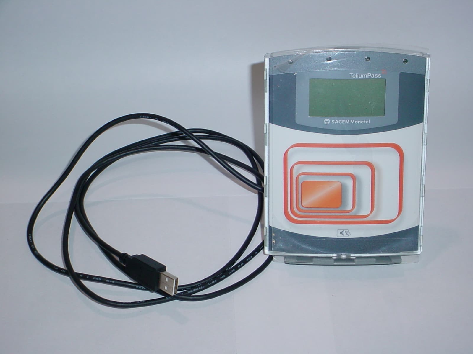
O3JNBS1200
Jan 27, 2008NBS1200
Equipment Class
DXT - Part 15 Low Power Transceiver, Rx Verified
O3JNBS5030
Dec 20, 2007WIRELESS POS TERMINAL BASE
Equipment Class
DSS - Part 15 Spread Spectrum Transmitter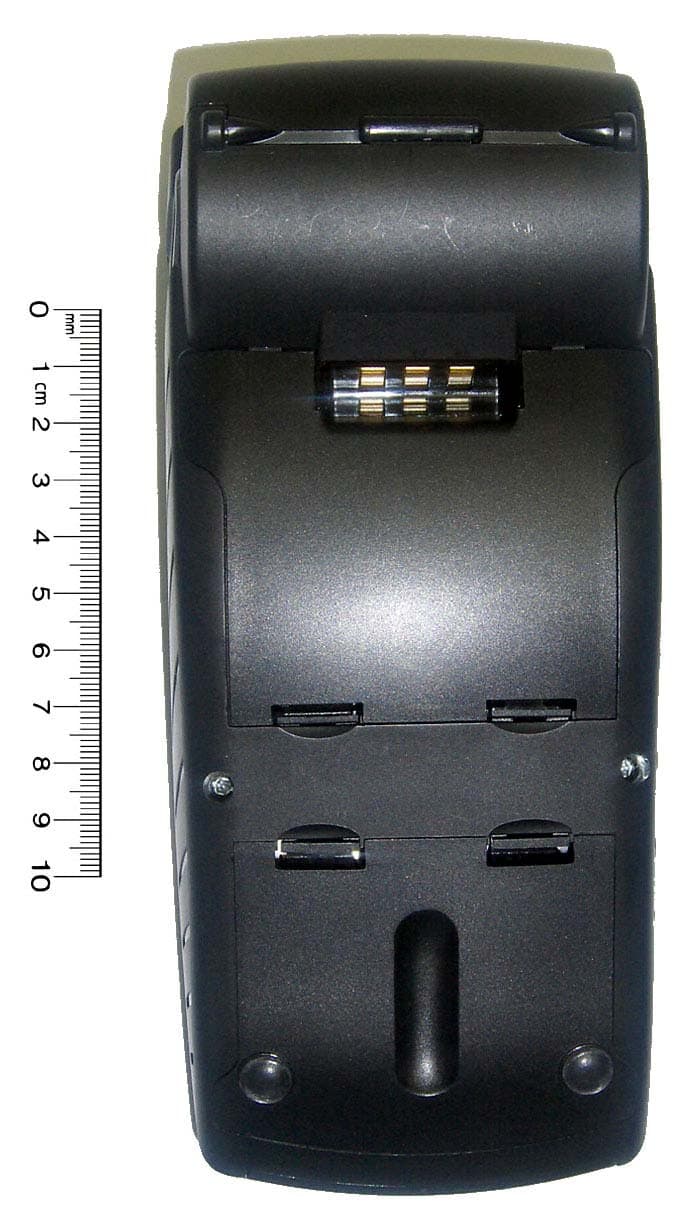
O3JNBS5700
Dec 20, 2007wireless pos terminal
Equipment Class
DSS - Part 15 Spread Spectrum Transmitter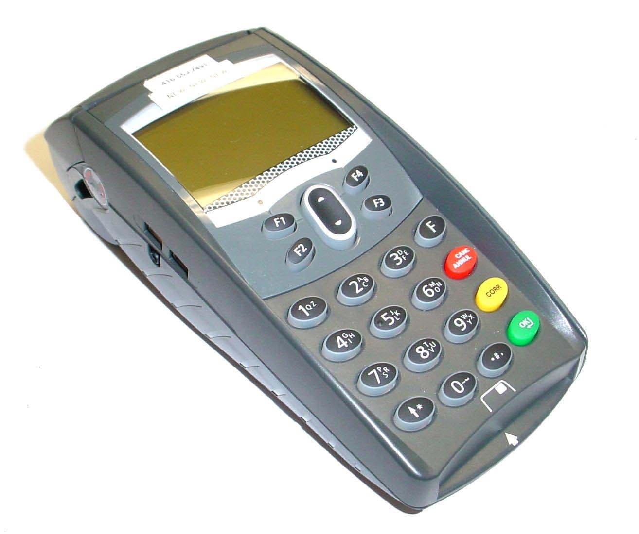
O3JNBS55XXB
Sep 06, 2007WIRELESS CDMA POINT-OF-SALE TERMINAL
Equipment Class
PCB - PCS Licensed Transmitter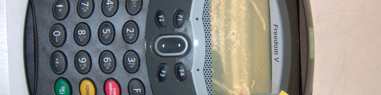
O3JNBS56XXT
Mar 16, 2006WIRELESS GSM/GPRS POINT-OF-SALE TERMINAL
Equipment Class
PCT - PCS Licensed Transmitter worn on body