O3JNBS56XXTWIRELESS GSM/GPRS POINT-OF-SALE TERMINAL
NBS Payment Solutions - Division of NBS Technologies Inc.
Click to zoom
Application Details
- Equipment Class
- PCT - PCS Licensed Transmitter worn on body
- Date of Grant
- Mar 16, 2006
- Application Purpose
- Original Equipment
- Date of Application
- Mar 16, 2006
- Equipment Note
- WIRELESS GSM/GPRS POINT-OF-SALE TERMINAL
- Frequency Range
- 1850.20000000 - 1909.80000000
- Country
- Canada
Documents & Files
Document Text
Text extracted from the exhibit documents filed with the FCC. Open a document above to read the original.
Users Manual
Tune Up procedures for Q2426. __________________________________________________________________________________ ________ This paper aims to explain the function of each radio parameters which are in the eeprom, the way to calculate each of them and the way to load them in the eeprom. - ThinDacValue : (former THIN_DAC_INIT_VALUE in the file EEPROM.H). The value given to this parameter is loaded in the 10 bits AFC DAC when the mobile is powered on. For more explanation about this parameter, have a look to the description of the parameter RoughDacValue below. The global excursion of the thin DAC is about 30 ppm, so the slope is about - 0.03 ppm for one step. It means that when the value loaded in the thin DAC is increased by one, the frequency of the VCXO decrease by 0.03 ppm. The thin DAC is used by the software to controle the frequency of the VCXO when the mobile is synchronised on the network to compensate doppler and temperature drift. - RoughDacValue : (former CARTE_DAC_INIT_VALUE in the file EEPROM.H). The value given to this parameter is loaded in the 8 bits DAC (GTI radio) 3 bits DAC (GISMO radio) when the mobile is powered on. This value should be such that the VCXO accuracy is better than 0.1 ppm at a temperature of 20 ° C when both ThinDacValue and RoughDacValue are loaded. The global excursion of the Rough DAC is about 80 ppm, so the slope is about + 0.3 ppm by step for GTI radio and + 10 ppm by step for GISMO radio. It means that when the value loaded in the rough DAC is increased by one the frequency of the VCXO increase by 0.3 ppm (GTI radio) 10 ppm (GISMO radio). The rough DAC is used by the software to compensate aging drift of VCXO. A good way to calculate the value to give to the parameters ThinDacValue and RoughDacValue, is to measure by any mean the frequency of the VCXO while the value loaded in the two DAC are half the excursion (512 for the thin DAC, 128 for the rough DAC for GTI radio, 4 for the rough DAC for GISMO radio). Then, calculate first the best value to give to RoughDacValue and then the best value to give to the ThinDacValue. As the slope of the rough DAC and of the thin DAC may vary around the value given, the whole process should be lead again one or two time. e.g : the measure of the VCXO give 13.0002 MHz ∆f/f = 200/13 E6 = +15.4 ppm For WISMO radio : The value loaded in the rough DAC should be decreased by (15.4 + 5) / 10 = 2 So RoughDacValue = 4 - 2 = 2. Then there is (15.4 - 10 x 2) = - 4.6 ppm left to be compensated with the thin DAC. To do so, the value loaded in the thin DAC should be decreased by 4.6 / 0.03 = 153. 1 So ThinDacValue = 512 - 180 = 358. - PwrVsAgcSlope : (former D_PWR_VS_AGC_SLOPE in the file EEPROM.H). This parameter is proportionate to the slope of the straight line describing the power on the antenna expressed in dBm versus the Agc value loaded in the 8 bits Agc DAC. To calculate the value to give to this parameter, multiply the previous slope by -128. Notice that PwrVsAgcSlope = 128x128 / AgcVsPwrSlope. e.g : if the slope is -0.4 dBm by Agc step, PwrVsAgcSlope = -128 x (-0.4) = 51. Notice that the straight line describing the power on the antenna versus the Agc must be built when the level on I and Q ADC is constant whatever the power on the antenna is. To do so, the nominal software can be used when synchronisation is possible. To make the synchronisation possible, the parameters ThinDacValue and RoughDacValue should be calculated as described and likely values should be given to the parameters PwrVsAgcSlope (e.g 51), AgcVsPwrSlope (e.g 320), BoardGain (e.g 40) and VoltageOrder (e.g 90). Then one can try to synchronise on a test set (e.g HP 8922) and tune the power and then read the Agc order for several value of power. The Agc order can be read in the top of the PC screen while using HAPC software. The right field is the second Agc field of the second line of the parameters displayed. It is just on the left of the Mkr field. Of course the value of the power on the antenna must be read on the test set and not in the Pwr field. Notice that the Mkr field should be rather constant while the power increase or decrease because of the software control even if the parameters are not good, however, the calculation may be improved by leading again the whole process using, the values obtained for PwrVsAgcSlope and AgcVsPwrSlope. - AgcVsPwrSlope : (former D_AGC_VS_PWR_SLOPE in the file EEPROM.H). This parameter is proportionate to the slope of the straight line describing the Agc value loaded in the 8 bits Agc DAC versus the power on the antenna expressed in dBm. To calculate the value to give to this parameter, multiply the previous slope by -128. e.g : if the slope is -2.5 Agc step by dBm , AgcVsPwrSlope = -128 x (-2.5) = 320. Notice that AgcVsPwrSlope = 128x128 / PwrVsAgcSlope. See above, description of the PwrVsAgcSlope. - VoltageOrder : (Former VOLTAGE_ORDER_VALUE in the file EEPROM.H). This parameter is expressed in step of Agc DAC. It allows to adjust the voltage on the I and Q kernel DAC egaliser entrance. The voltage should be about 1 V pp. If VoltageOrder is increased by one, the voltage on I and Q increased by about 0.05 V. To calculate the right value, give a likely value to this parameter, and measure the voltage when the mobile is synchronised (see the process described for the calculation of the parameter PwrVsAgcSlope). Then measure the voltage on the kernel DAC egaliser entrance and adjust the value of VoltageOrder until the right voltage is obtained. 2 Notice that when a voltage of 1 Vpp on I and Q kernel entrance is obtained, the parameter Mkr displayed on the screen while using the HAPC software should be about 20. If not, there certainly some hardware trouble. - BoardGain : (Former BOARD_SPECIFIC_GAIN in the file EEPROM.H). This parameter is expressed in dB and corresponds to the gain of the radio reception channel. To calculate this parameter, a mean value being given to BoardGain (e.g 40), try to synchronise on a …
Text truncated - open the document above for the full version.
Users Manual
WISMO Quik Q2400 series Q2406 and Q2426 Product Specification Reference: WM_PRJ_Q2400_PTS_002 Revision: 004 Date: March 5, 2004 confidential © Page : 1 / 63 This document is the sole and exclusive property of WAVECOM. Not to be distributed or divulged without prior written agreement. Ce document est la propriété exclusive de WAVECOM. Il ne peut être communiqué ou divulgué à des tiers sans son autorisation préalable. WM_PRJ_Q2400_PTS_002 - 004 March 5, 2004 Document Information Revision Date History of the evolution 001 24 Oct 02 Creation (Preliminary version) 002 24 Jan. 03 Remove “Preliminary” status. Modification in applicable products list: • Add Q2406D and Q2426D products and Q2406E and Q2426E products • Remove Q2406C and Q2426C products Update sensitivity value for GSM850 and EGSM900 RF bands. Update mechanical drawing. 003 14 Apr 03 Extract of Design guidelines information 004 March 5, 2004 FCC wording for starter kit approval and not modular approvalGulmit Sobti confidential © Page : 2 / 63 This document is the sole and exclusive property of WAVECOM. Not to be distributed or divulged without prior written agreement. Ce document est la propriété exclusive de WAVECOM. Il ne peut être communiqué ou divulgué à des tiers sans son autorisation préalable. WM_PRJ_Q2400_PTS_002 - 004 March 5, 2004 Contents Document Information......................................................................................................................................................................2 Contents..............................................................................................................................................................................................3 Caution 6 Trademarks...........................................................................................................................................................................................6 Overview 7 Reference documents.......................................................................................................................................................................8 1 General description................................................................................................................................................................9 1.1 General information..................................................................................................................9 1.2 Functional description............................................................................................................ 10 1.2.1 RF functionalities..........................................................................................................11 1.2.2 Baseband functionalities..............................................................................................11 1.3 Firmware.................................................................................................................................12 2 Interfaces..............................................................................................................................................................................13 2.1 General Purpose Connector (GPC).......................................................................................13 2.2 Power supply..........................................................................................................................14 2.2.1 General description......................................................................................................14 2.2.2 Power consumption......................................................................................................15 2.3 Electrical information for digital I/O.........................................................................................17 2.4 LCD interface..........................................................................................................................18 2.4.1 SPI bus 18 2.4.2 Two-wire interface........................................................................................................18 2.5 SPI Auxiliary bus....................................................................................................................18 2.6 Keyboard interface.................................................................................................................19 2.7 Main serial link (UART1)........................................................................................................20 2.8 Auxiliary serial link (UART2)...................................................................................................20 2.9 SIM interface..........................................................................................................................21 2.9.1 General Description......................................................................................................21 2.9.2 SIM 3/5V management.................................................................................................22 2.10 General Purpose Input/Output...............................................................................................23 confidential © Page : 3 / 63 This document is the sole and exclusive property of WAVECOM. Not to be distributed or divulged without prior written agreement. Ce document est la propriété exclusive de WAVECOM. Il ne peut être communiqué ou divulgué à des tiers sans son autorisation préalable. WM_PRJ_Q2400_PTS_002 - 004 March 5, 2004 2.11 Activity status indication.........................................................................................................23 2.12 Analog to Digital Converter (ADC).........................................................................................24 2.13 Audio interface 25 2.13.1 Microphone inputs........................................................................................................25 2.13.1.1 Common microphone inputs characteri…
Text truncated - open the document above for the full version.
Attestation Statements
1 Equipment Under Test General Information Form File Number: MIS-052 Applicant’s complete, legal business name: NBS Technologies Inc. Applicant’s IC Company Number (CN): 2279B-NBS56XXT Applicant’s FCC Registration Number (FRN): O3JNBS56XXT Applicant’s mailing address: Street Address: 703 Evans Ave., Suite 400 City: Toronto Province/State: Ontario Country: Canada Postal/Zip Code: M9C 5E9 Applicant Contact Person: Name: Dragoslav Jovanovic Title: Manager Hardware Development Telephone: 416 621 1911 Fax No.: 416 621 8875 E-mail: [email protected] Manufacturer’s complete, legal business name: SAGEM Monetel Manufacturer’s mailing address: Street Address: 1, Rue Claude Chappe – BP346 City: Guilherand-Granges Province/State: Country: France Postal/Zip Code: 07503 Manufacturer Contact Person: Name: Clement Lormeau Title: Customer Service Telephone: +33 4 75 81 40 47 Fax No.: +33 4 75 81 41 57 E-mail: [email protected] Equipment Under Test (EUT) Information: Marketing Name of EUT: NBS5600 Description: Wireless POS Terminal Model(s) No.: NBS5600 Serial No.: NAXXXXXX External Power Supply: 5V/1A Transmitting/Receiving Antenna Type: [√ ] Integral [ ] Non-Integral Primary User Functions of EUT: Financial Transactions 2 EUT’S Technical Specifications: TRANSMITTER Equipment Type: [√ ] Portable [ ] Mobile [ ] Base station (fixed use) Intended Operating Environment: [ ] Residential [√ ] Commercial, industrial or business environment Power Supply Requirement: 3.6VDC RF Output Power Rating: 2W E-GSM 900/GSM 850, 1W GSM 1800/1900 Operating Frequency Range: Band 0: 824-849MHz Band 1: 1850-1910MHz RF Output Impedance: 50 Ohms Channel Spacing (if applicable): Type of Emissions: Data rate: Type of modulation on the transmitter carrier: Nature of signal(s) modulating the main carrier: Type of transmitter information: Oscillator Frequency(ies): Terminal: 32kHz(quartz), 20MHz(quartz), 57MHz(PLL) Base station: 12.288MHz(quartz), 2.048MHz(PLL) Antenna Connector Type: [ ] BNC [ ] N [ ] TNC [ ] SMA [ ] Integral [√ ] Other, Specify: U.FL-R-SMT (internal) Antenna Description (if more than one antenna, provide a list of all the antennas to be used with the device): Manufacturer: SAGEM Monetel Type: Dual band Model: 2519132244AA Frequency Range: 824-894MHz, 1850-1990Mhz Gain (dBi): 0 RECEIVER Equipment Type: [√ ] Portable [ ] Mobile [ ] Base station (fixed use) Power Supply Requirement: 3.6VDC Operating Frequency Range: Band 0: 869-894MHz Band 1: 1930-1990MHz RF Input Impedance: 50 Ohms Intermediate Frequency(ies): Oscillator Frequency(ies): 3 List of EUT’s Ports: Port Number EUT’s Port Description Number of Identical Ports Connector Type Cable Type (Specify minimum length and shielded/non-shielded) 1 2 3 4 5 6 7 8 9 10 NOTES: Ports, which are not connected to cables during normal intended operation (for factory/technical services uses only): USB (2), headphone [ ] None OR List all EUT ports not connected during tests Explanation
Cover Letter(s)
February 28, 2006 FEDERAL COMMUNICATIONS COMMISSION 7435 Oakland Mills Road Columbia, MD 21046 U.S.A. Subject: Request for withholding from public disclosure the schematic diagrams and system block diagrams pursuant to an application for certification. Applicant: NBS Technologies Inc. Product: NBS56XX Model: NBS56XXTXXX FCC ID: O3JNBS56XXT Dear Sir/Madam, We, NBS Technologies Inc., requests that the following information submitted with the application for Equipment Authorization be withheld from public disclosure as per Section 0.459 of the Commission's Rules: 1. Block Diagram 2. Schematics 3. Operational Description 4. Parts List This request is made under the provisions of Section 0.457(d) of the Commission's Rules, and Section 552(b)(4) of the Freedom of Information Act. These sections authorize withholding from public inspection materials, which would be privileged as a matter of law if retained by the person submitting them, and materials which would not customarily be released to the public by that person. If you have any queries, please do not hesitate to contact us: OUR TELEPHONE NO.: 1 416 621 1911 Yours truly, Dragoslav Jovanovic Manager Hardware Development NBS Technologies Inc.
External Photos
ANNEX 2 – EXTERNAL PHOTOGRAPHS NBS Technologies Inc. NBS56XX, Model: NBS56XXTXXX FCC ID: O3JNBS56XXT IC: 2279B-NBS56XXT Photo # A2 - 1 ANNEX 2 – EXTERNAL PHOTOGRAPHS NBS Technologies Inc. NBS56XX, Model: NBS56XXTXXX FCC ID: O3JNBS56XXT IC: 2279B-NBS56XXT Photo # A2 - 2 ANNEX 2 – EXTERNAL PHOTOGRAPHS NBS Technologies Inc. NBS56XX, Model: NBS56XXTXXX FCC ID: O3JNBS56XXT IC: 2279B-NBS56XXT Photo # A2 - 3 ANNEX 2 – EXTERNAL PHOTOGRAPHS NBS Technologies Inc. NBS56XX, Model: NBS56XXTXXX FCC ID: O3JNBS56XXT IC: 2279B-NBS56XXT Photo # A2 - 4 ANNEX 2 – EXTERNAL PHOTOGRAPHS NBS Technologies Inc. NBS56XX, Model: NBS56XXTXXX FCC ID: O3JNBS56XXT IC: 2279B-NBS56XXT Photo # A2 - 5
ID Label/Location Info
1 01/03/2006 Product Name: NBS56XX Model: NBS56XXTXXX Terminal Label NBS5600 Model:NBS5601T001 HW: ECL Y SW: 0929-0704-Y FCC ID: O3JNBS56XXT IC: 2279B-NBS56XXT M ade in/Fait au: France llllllllllllllllllllllllllllllllll NBS S/N: NAXXXXXX lllllllllllllllllllllllllllllllllll XXXXXXXXX lllllllllllllllllllllllllllllllllll XXXXXXXXXXXXXXXX lllllllllllllllllllllllllllllllll GPRS S/N: MFD: XX/XXXX Model number explanation NBS 5 6 XX T XXX Brand Name Configuration: 001 = Black, TD Bank logo Product Family 002 = Black, No logo 003 = Communication Type Device Type: 0 = No Radio A = Accessories 5 = CDMA Radio B = Base 6 = GPRS Radio K = Kit 7 = Bluetooth Radio P = PINpad 8 = Wi-Fi Radio T = Terminal Hardware variations: 00 = Basic (MSR, Smart Card, MMC, SAM, USB) 2 Terminal Label location Terminal label with FCC and IC ID
ID Label/Location Info
Q2426 FCC ID Location
ID Label/Location Info
Q2426 FCC ID label FCC ID: O9EQ2426-SK
Internal Photos
ANNEX 3 – INTERNAL PHOTOGRAPHS NBS Technologies Inc. NBS56XX, Model NBS56XXTXXX FCC ID: O3JNBS56XXT IC: 2279B-NBS56XXT A2 - 1 ANNEX 3 – INTERNAL PHOTOGRAPHS NBS Technologies Inc. NBS56XX, Model NBS56XXTXXX FCC ID: O3JNBS56XXT IC: 2279B-NBS56XXT A2 - 2 ANNEX 3 – INTERNAL PHOTOGRAPHS NBS Technologies Inc. NBS56XX, Model NBS56XXTXXX FCC ID: O3JNBS56XXT IC: 2279B-NBS56XXT A2 - 3
Internal Photos
ANNEX 3 – INTERNAL PHOTOGRAPHS NBS Technologies Inc. NBS56XX, Model NBS56XXTXXX FCC ID: O3JNBS56XXT IC: 2279B-NBS56XXT A2 - 4 ANNEX 3 – INTERNAL PHOTOGRAPHS NBS Technologies Inc. NBS56XX, Model NBS56XXTXXX FCC ID: O3JNBS56XXT IC: 2279B-NBS56XXT A2 - 5 ANNEX 3 – INTERNAL PHOTOGRAPHS NBS Technologies Inc. NBS56XX, Model NBS56XXTXXX FCC ID: O3JNBS56XXT IC: 2279B-NBS56XXT A2 - 6
Internal Photos
ANNEX 3 – INTERNAL PHOTOGRAPHS NBS Technologies Inc. NBS56XX, Model NBS56XXTXXX FCC ID: O3JNBS56XXT IC: 2279B-NBS56XXT A2 - 7 ANNEX 3 – INTERNAL PHOTOGRAPHS NBS Technologies Inc. NBS56XX, Model NBS56XXTXXX FCC ID: O3JNBS56XXT IC: 2279B-NBS56XXT A2 - 8 ANNEX 3 – INTERNAL PHOTOGRAPHS NBS Technologies Inc. NBS56XX, Model NBS56XXTXXX FCC ID: O3JNBS56XXT IC: 2279B-NBS56XXT A2 - 9 ANNEX 3 – INTERNAL PHOTOGRAPHS NBS Technologies Inc. NBS56XX, Model NBS56XXTXXX FCC ID: O3JNBS56XXT IC: 2279B-NBS56XXT A2 - 10 ANNEX 3 – INTERNAL PHOTOGRAPHS NBS Technologies Inc. NBS56XX, Model NBS56XXTXXX FCC ID: O3JNBS56XXT IC: 2279B-NBS56XXT A2 - 11
Parts List/Tune Up Info
March 07, 2006 UltraTech Engineering Labs Inc. 3000 Bristol Circle Oakville, Ontario, L6H 6G4 Canada Subject: Tune-up procedure Applicant: NBS Technologies Inc. Product: NBS56XX Model: NBS56XXTXXX Dear Sir/Madam, I certify that this device does not have a tuning procedure; the RF output power and channel frequencies are programmed in the Q2426B RF module firmware by Wavecom. Regards, Dragoslav Jovanovic Manager Hardware Development NBS Technologies Inc.
RF Exposure Info
w w w . n b s t e c h . c o m 4 Product Regulatory Information FCC RF Exposure Requirements: SAR compliance for body- worn operations is restricted to belt-clips, holsters, and accessories that have no metallic component in the assembly and which provide at least 1 cm separation between the device, including its antenna, and the users body. Changes or modifications to this unit not expressly approved by NBS Technologies Inc. could void the user’s authority to operate this equipment. Manufacturer’s Declaration of Conformit y A m e r i c a n N o t i c e FCC Part 15 (USA) Compliance (EMC) This device complies with the requirements in Part 15 of the FCC Rules for a Class B digital device. Operation is subject to the following two conditions: • This device may not cause harmful interference. • This device must accept any interference received, includ- ing interference that may cause undesired operation. Note: This equipment has been tested and found to comply with the limits of a Class B digital device, pursuant to part 15 of the FCC Rules. These limits are designed to provide reasonable protection against harmful interference in a residential in- stallation. This equipment generates, uses and can radiate radio frequency energy and, if not installed and used in accordance with the instructions, may cause harmful interference to radio communications. However, there is no guarantee that in- terference will not occur in a particular installation. If this equip- ment does cause harmful interference to radio or television re- ception, which can be determined by turning the equipment off and on, the user is encouraged to try to correct the interference by one or more of the following measures: • Reorient or relocate the receiving antenna. • Increase the separation between the equipment and re-
RF Exposure Info
UltraTech Group of Labs 31040/SIT C-1376 46390-2049 200093-0 2 00-034 SL2-IN-E-1119R 3000 Bristol Circle, Oakville, Ontario, Canada L6H 6G4 Tel.: (905) 829-1570 Fax.: (905) 829-8050 Website: www.ultratech-labs.com Email: [email protected] March 08, 2006 NBS Technologies Inc. 703 Evans Ave., Suite 400 Toronto, ON Canada M9C 5E9 Attn.: Mr. Dragoslav Jovanovic Subject: Verification Testing in accordance with SAR (Specific Absorption Rate) requirements using guidelines established in: IEEE C95.1-1991, FCC OET Bulletin 65 (Supplement C) Industry Canada RSS-102 (Issue 2) ACA Radiocommunications (Electromagnetic Radiation – Human Exposure) Amendment Standard 2000 (No. 1) Product: Wireless POS Terminal Model: NBS5600 Dear Mr. Jovanovic The product sample has been tested in accordance with SAR (Specific Absorption Rate) requirements using guidelines established in IEEE C95.1-1991, FCC OET Bulletin 65 (Supplement C), Industry Canada RSS-102 (Issue 2)and ACA Radiocommunications (Electromagnetic Radiation – Human Exposure) Amendment Standard 2000 (No. 1), and the results and observation were recorded in the engineering report, Our File No.: MIS-052-SAR Enclosed you will find a copy of the engineering report. If you have any queries, please do not hesitate to contact us. Yours truly, Tri Minh Luu, P.Eng Vice President - Engineering Encl. March 08, 2006 File No.: MIS-052-SAR NBS Technologies Inc. 703 Evans Ave., Suite 400 Toronto, ON CANADA M9C 5E9 NOT TRANSFERABLE This Verification Certificate is hereby issued to the named GRANTEE and is VALID ONLY for the equipment identified hereon for use under the rules and regulations listed below: GRANTEE'S NAME: NBS Technologies Inc. PRODUCT UNDER TEST: Wireless POS Terminal MODEL NO.: NBS5600 FCC ID: O3JNBS56XXT OPERATING FREQUENCY RANGE: 824.2 ~ 848.8 MHz (GSM 850) 1850.2 ~ 1909.8 MHz (GSM 1900) MEASURED RF OUTPUT POWER: 1.823 W / 1.61 W ERP (GSM 850) 0.863 W / 1.42 W EIRP (GSM 1900) DEVICE CATEGORY: Portable EXPOSURE CATEGORY: General Population/Uncontrolled MAX. PEAK SPATIAL-AVERAGE SAR 1g : 0.88 W/Kg This wireless portable device has been shown to be compliant for Specific Absorption Rate (SAR) for General Population/Uncontrolled exposure limit. APPLICABLE STANDARDS: SAR (Specific Absorption Rate) requirements using guidelines established in IEEE C95.1-1991, FCC OET Bulletin 65 (Supplement C Edition 01-01), Industry Canada RSS-102(Issue 2) and ACA Radiocommunications (Electromagnetic Radiation – Human Exposure) Amendment Standard 2000 (No. 1) Approved by: Tri M. Luu, P.Eng. V.P. – Engineering UltraTech 3000 Bristol Circle, Oakville, Ontario, Canada, L6H 6G4 Tel.: (905) 829-1570 Fax.: (905) 829-8050 Website: www.ultratech-labs.com Email: [email protected], Email: [email protected] 2 31040/SIT C-1376 46390-2049 200093-0 SL2-IN-E-1119R 00-034 Wireless POS Terminal Model No.: NBS5600 Tested For NBS Technologies Inc. 703 Evans Ave., Suite 400 Toronto, ON Canada M9C 5E9 In Accordance With SAR (Specific Absorption Rate) Requirements using guidelines established in IEEE C95.1-1991, FCC OET Bulletin 65 (Supplement C), Industry Canada RSS-102(Issue 2) and ACA Radiocommunications (Electromagnetic Radiation – Human Exposure) Amendment Standard 2000 (No. 1) UltraTech's File No.: MIS-052-SAR This Test report is Issued under the Authority of Tri M. Luu, Professional Engineer, Vice President of Engineering UltraTech Group of Labs Date: March 08, 2006 Report Prepared by: JaeWook Choi Tested by: Carolyn Luu Issued Date: March 08, 2006 Test Dates: February 15 - 16, 2006 The results in this Test Report apply only to the sample(s) tested, which has been randomly selected. UltraTech 3000 Bristol Circle, Oakville, Ontario, Canada, L6H 6G4 Telephone (905) 829-1570 Facsimile (905) 829-8050 Website: www.ultratech-labs.com Email: [email protected] SPECIFIC ABSORPTION RATE (SAR) Page 1 IEEE C95.1-1991, FCC OET Bulletin 65 (Supplement C), Industry Canada RSS-102(Issue 2) and ACA Radiocommunications (Electromagnetic Radiation – Human Exposure) Amendment Standard 2000 (No. 1) Wireless POS Terminal M/N: NBS5600 FCC ID: O3JNBS56XXT ULTRATECH GROUP OF LABS File #: MIS-052-SAR 3000 Bristol Circle, Oakville, Ontario, Canada L6H 6G4 March 08, 2006 Tel. #: 905-829-1570, Fax. #: 905-829-8050, Email: [email protected], Website: http://www.ultratech-labs.com • Assessed by ITI (UK) Competent Body, NVLAP (USA) Accreditation Body & ACA/AUSTEL (Australia), VCCI (Japan) • Accredited by Industry Canada (Canada) under ACC-LAB (Europe/Canada MRA and APEC/Canada MRA) • Recognized/Listed by FCC (USA ) • All test results contained in this engineering test report are traceable to National Institute of Standards and Technology (NIST) TABLE OF CONTENTS EXHIBIT 1. INTRODUCTION ................................................................................................................................................ 5 1.1. SCOPE ............................................................................................................................................................................... 5 1.2. REFERENCES................................................................................................................................................................... 5 EXHIBIT 2. PERFORMANCE ASSESSMENT ..................................................................................................................... 6 2.1. CLIENT AND MANUFACTURER INFORMATION ...................................................................................................... 6 2.2. DEVICE UNDER TEST (D.U.T.) DESCRIPTION.............................................................................................................. 6 2.3. LIST OF D.U.T.’S ACCESSORIES:.................................................................................................................................. 7 2.4. SPECIAL CHANGES ON THE D.U.T.’S HARDWARE/SOFTWARE FOR TESTING PURPOSES ................…
Text truncated - open the document above for the full version.
RF Exposure Info
INSTALLATION AND INSTRUCTION MANUAL INCLUDING HUMAN EXPOSURE STATEMENT As required by § 2.1033(c)(3), here is a part of the User's Guide and Technical Manual" that describes modem features, installation, and operation. Also provided, on page 52 of our User’s Manual, is a statement addressing human exposure to radio frequency radiation. This information is necessary to ensure that equipment installers, operators and users are made aware of the dangers of exposure to radio frequency radiation and that the Modem is installed and operated in compliance with 47 CFR Part 24, Subpart E of the FCC Rules and Regulations. Pursuant to § 24.52 RF hazards, all emissions from the Modem, both fundamental and unwanted, are subject to the radio frequency radiation exposure requirements given in § 1.1307(b), § 2.1091 and § 2.1093, as appropriate. For fixed transmitters, § 1.1307(b) requires the preparation of an Environmental Assessment (EA) if the transmitter would cause human exposure to levels of radio frequency radiation in excess of the applicable limits given in § 1.1310. However, determination of compliance with these limits and preparation of an EA if they are exceeded is required only for licensed PCS facilities, operations and transmitters with the following characteristics: 1. Non-building-mounted antennas: height above ground level to lowest point of antenna < 10m and total power of all channels > 2000 W ERP (3280 W EIRP) 2. Building-mounted antennas: total power of all channels > 2000 W (3280 W EIRP) "Fixed" in this context means that the device is physically secured at one location and is not able to be easily moved to another location. Since the modem transmits on a single channel with a maximum peak output power of 1.0 W (30 dBm) nominal, the maximum specified antenna gain of 7 dBi results in a maximum peak e.i.r.p. of 37 dBm (5.0 W), well below the level which would trigger a routine environmental evaluation. Therefore, in fixed applications, the modem is categorically excluded from performance of a routine environmental evaluation or preparation of an EA. In § 2.1091(b), a mobile device is defined as a transmitting device designed to be used in other than fixed locations and to generally be used in such a way that a separation distance of at least 20 centimeters is normally maintained between the transmitter's antenna and the body of the user or nearby persons. In accordance with § 2.1091(c), mobile PCS devices are categorically excluded from routine environmental evaluation for RF exposure prior to equipment authorization or use if their e.i.r.p. is less than 3 W (34.8 dBm)…
Text truncated - open the document above for the full version.
Contact Information
Applicant
Dragoslav Jovanovic(Manager, Engineering)
Test Firm
UltraTech Engineering Labs Inc.Tri Luu
Technical Specifications
| # | Rule Parts | Frequency Range | Power Output | Emission | Tolerance |
|---|---|---|---|---|---|
| 2 | 24E | 1.85 GHz - 1.91 GHz | 1.42 W | 243KGXW | 2.5 ppm |
Other Applications from NBS Payment Solutions - Division of NBS Technologies Inc.
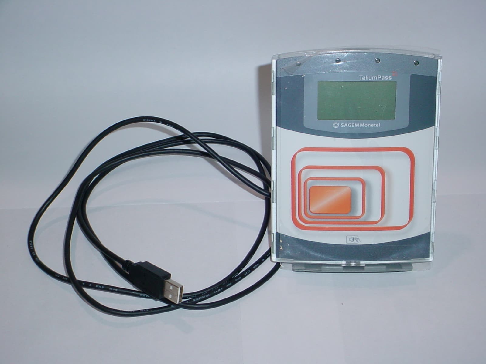
O3JNBS1200
Jan 27, 2008NBS1200
Equipment Class
DXT - Part 15 Low Power Transceiver, Rx Verified
O3JNBS5030
Dec 20, 2007WIRELESS POS TERMINAL BASE
Equipment Class
DSS - Part 15 Spread Spectrum Transmitter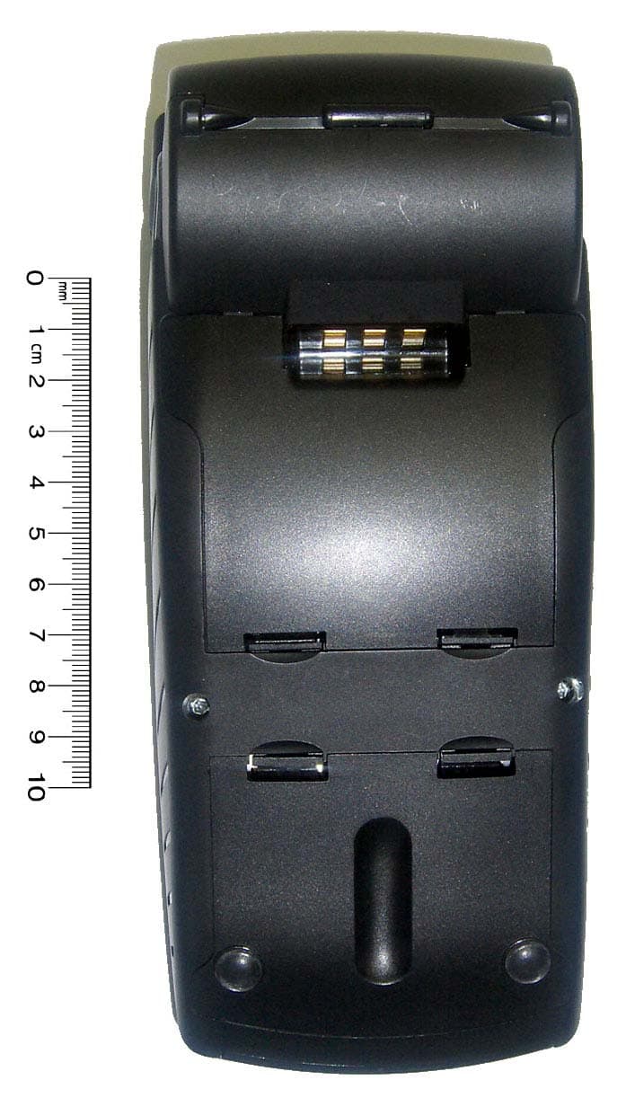
O3JNBS5700
Dec 20, 2007wireless pos terminal
Equipment Class
DSS - Part 15 Spread Spectrum Transmitter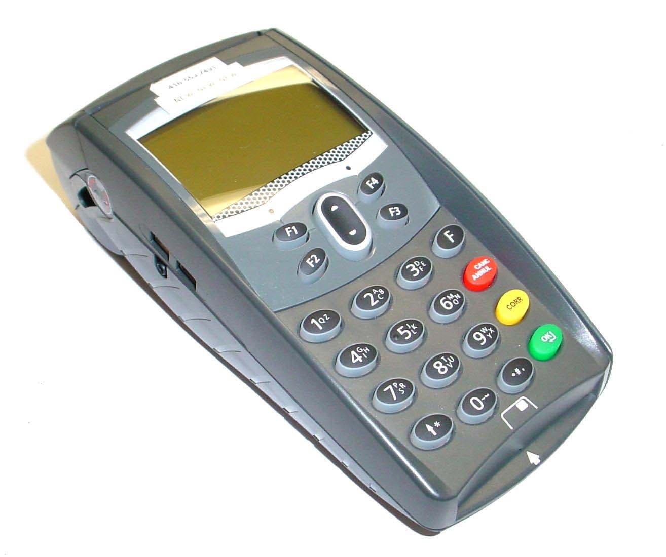
O3JNBS55XXB
Sep 06, 2007WIRELESS CDMA POINT-OF-SALE TERMINAL
Equipment Class
PCB - PCS Licensed Transmitter
O3JNBS55XXT
May 26, 2005Wireless CDMA Point-of-Sale Terminal
Equipment Class
PCT - PCS Licensed Transmitter worn on body