OIWCBDAPS910W80Bi-Directional Amplifier and Booster
Dekolink Wireless Ltd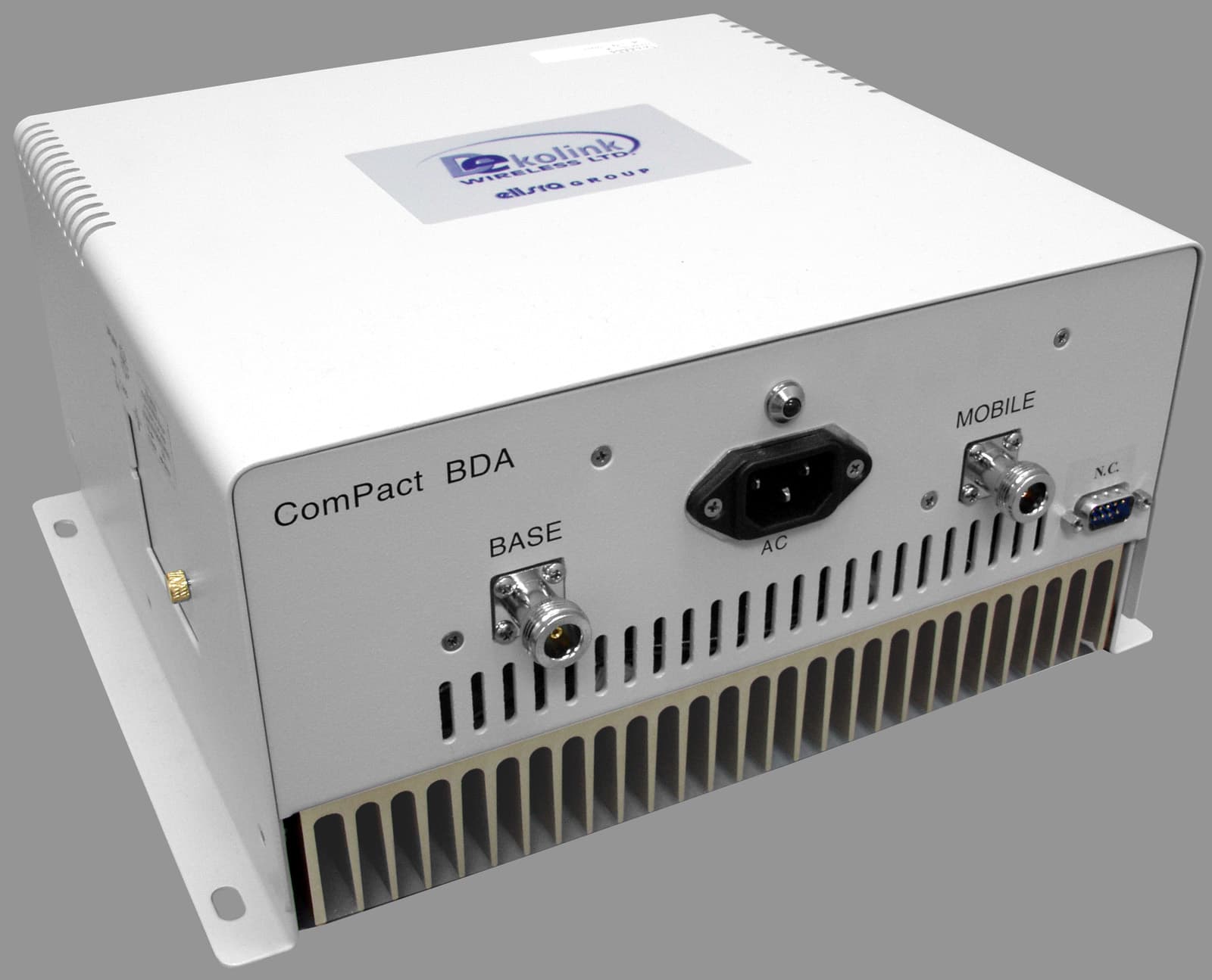
Click to zoom
Application Details
- Equipment Class
- AMP - Amplifier
- Date of Grant
- Jun 11, 2003
- Application Purpose
- Original Equipment
- Date of Application
- Jun 11, 2003
- Equipment Note
- Bi-Directional Amplifier and Booster
- Frequency Range
- 935.00000000 - 940.00000000
- Company
- Dekolink Wireless Ltd
- Country
- Israel
Documents & Files
Document Text
Text extracted from the exhibit documents filed with the FCC. Open a document above to read the original.
Users Manual
Dekolink Wireless Ltd.;16 Bazel St.Qiryat-Arieh Petah-Tikva Israel, 49510 Tel- 972-3-9180-180; Fax-972-3-190-9180; [email protected] INSTALLATION AND OPERATING INSTRUCTIONS FOR MW-CBDA SERIES 10W-80-A COMPACT BI-DIRECTIONAL AMPLIFIERS ; Web site- www.dekolink.com r ev 5 11/ 02 page 1 of 12 Dekolink Wireless Ltd.;16 Bazel St.Qiryat-Arieh Petah-Tikva Israel, 49510 Tel- 972-3-9180-180; Fax-972-3-190-9180; [email protected] INSTALLATION & OPERATING INSTRUCTIONS CBDA 10W-80-A COMPACT BI-DIRECTIONAL AMPLIFIERS TABLE OF CONTENTS PARAGRAPH PAGE No BDA OVERVIEW 3 BLOCK DIAGRAM DESCRIPTION 3 STEP ATTENUATOR & RF GAIN & SETTING 4 AGC FUNCTION 5 AGC & GAIN CONTROLS 5 BDA INSTALLATION 6 BASE/DONOR ANTENNA INSTALLATION 6 REMOTE/MOBILE ANTENNA INSTALLATION 6 ANTENNA ISOLATION 6 INSTALLATION STEPS 7 DIAGNOSTICS GUIDE 8 ELECTRICAL SPECIFICATIONS 9 SYSTEM FREQUENCY RANGE 9 ENVIRONMENTAL CONDITIONS 10 MECHANICAL SPECIFICATIONS 10 RF EXPOSURE WARNING 10 LIMITED WARRANTY 12 LIST OF DRAWINGS DRAWING PAGE No BDA RF BLOCK DIAGRAM 4 AGC AMPLIFIER 5 MECHANICAL OUTLINE 11 ; Web site- www.dekolink.com r ev 5 11/ 02 page 2 of 12 Dekolink Wireless Ltd.;16 Bazel St.Qiryat-Arieh Petah-Tikva Israel, 49510 Tel- 972-3-9180-180; Fax-972-3-190-9180; [email protected] :BDA OVERVIEW The Compact Bi-Directional Amplifier (CBDA) assembly provides an exceptional repeater/booster performances to extend the coverage area of radio communications in buildings and RF shielded environments. Features such as high linearity power amplifiers are contributing for the overall improved system linearity performances. The unit is based on a duplexed path configuration, having sharp out of band attenuation for improved isolation between the receiving and transmitting paths. :BLOCK DIAGRAM DESCRIPTION The CBDA Downlink path receives the RF signals from base station amplifies them and transmits them to the subscriber. The BDA Uplink path receives the RF signals from the subscriber amplifies them and transmits them to the base station. Two duplexers frequency separate the signals to the proper amplifying path and isolate the two signals. For each path two amplifiers do the path signal amplification; a low noise amplifier (LNA) and a high power amplifier. The low noise amplifier has a 30 dB step attenuator at its output. The step attenuator is used to set the BDA repeater gain. The power amplifiers in the BDA have an AGC option switch. When switched on, the AGC circuit limits the amplifier output power. The AGC circuit senses the output power and introduces more attenuation, when the output power exceeds the preset level. This way the gain of the amplifier is reduced, its output power is limited and the intermodulations products are kept below the desired level. The AGC amplifier has a Power LED lamp that illuminates when the output power has reached the preset power limit. ; Web site- www.dekolink.com r ev 5 11/ 02 page 3 of 12 Duplexer Downlink Duplexer Uplink LNA Attenuator Power Monitor PA AGC LNA Attenuator Power Monitor PA AGC BDA RF BLOCK DIAGRAM TO BASE TO MOBILE Dekolink Wireless Ltd.;16 Bazel St.Qiryat-Arieh Petah-Tikva Israel, 49510 Tel- 972-3-9180-180; Fax-972-3-190-9180; [email protected] ; Web site- www.dekolink.com r ev 5 11/ 02 page 4 of 12 Step Attenuator & RF Gain Setting For proper operation of the BDA; the isolation between the base station antenna and the mobile antenna should exceed the BDA gain by at least 12 dB. If the BDA gain were higher than the isolation between the antennas, oscillation would start and would saturate the amplifier. Isolation few dB higher than the BDA gain cannot start oscillations but would cause gain ripple in the band. The step attenuator on the low noise amplifier can reduce the BDA gain. The BDA gain can be stepped down by the amount indicated on the step attenuator. Dekolink Wireless Ltd.;16 Bazel St.Qiryat-Arieh Petah-Tikva Israel, 49510 Tel- 972-3-9180-180; Fax-972-3-190-9180; [email protected] AGC FUNCTION The BDA has AGC function on both paths that serve to prevent the saturation of the power amplifier. Their amplifier has a directional coupler and a detector at the output of the high power amplifier to monitor the output power. When a high signal is received the automatic level control detects the amplitude and sends a feedback signal to a voltage variable attenuator which attenuates the signal level so that the output power of the amplifier does not exceed the preset limit. The LED on the amplifier illuminates when the power out the amplifier is within the set limit (when the AGC is On and when the AGC is OFF). The switch on the RF amplifier enables the AGC function. If the AGC is disabled then the amplifier gives maximum gain. AGC AND GAIN CONTROLS The AGC and GAIN SETTING functions for the up link path are reached by opening the small slide door located on the CBDA left side, adjacent to the BASE antenna port. For the down link path the door is on the right side adjacent to the MOBILE antenna port RF Power LED : The LED illuminates when the output power exceeds the AGC Set . AGC ON / OFF Switch : When OFF the amplifier works with its highest gain (AGC Function OFF). When set to ON (AGC Function ON) the amplifier power output cannot exceed the set limit. Gain setting: By using the rotary knob , the attenuation can be adjusted in 2 dB steps. ; Web site- www.dekolink.com r ev 5 11/ 02 page 5 of 12 Dekolink Wireless Ltd.;16 Bazel St.Qiryat-Arieh Petah-Tikva Israel, 49510 Tel- 972-3-9180-180; Fax-972-3-190-9180; [email protected] BDA INSTALLATION Install the BDA Repeater in a shielded, ventilated and easy to reach area. Use low loss cables to connect antennas to the BDA. Install the BDA close to the service area to improve output power and noise figure. Mount the BDA with RF connecters pointing down. The RF connection is made via two type “N” female connectors. The RF connector labeled “Base” must be connected to the antenna; usu…
Text truncated - open the document above for the full version.
Users Manual
Dekolink Wireless Ltd., 16 Bazel St., Qiryat-Arieh Petah-Tikva Israel, 49510 Tel: 972-3-9180-180; Fax: 972-3-190-9180 Email: [email protected] INSTALLATION AND OPERATING INSTRUCTIONS FOR MW-IBDB-10W40-PS9 BOOSTER ; Web site: www.dekolink.com Rev 0 02/03 Page 1 of 9 Dekolink Wireless Ltd., 16 Bazel St., Qiryat-Arieh Petah-Tikva Israel, 49510 Tel: 972-3-9180-180; Fax: 972-3-190-9180 Email: [email protected] TABLE OF CONTENTS PARAGRAPH PAGE No BOOSTER OVERVIEW 3 BLOCK DIAGRAM DESCRIPTION 3 BOOSTER OPERATION 4 AGC FUNCTION 4 AGC AND GAIN CONTROLS 5 ELECTRICAL SPECIFICATIONS 6 ENVIRONMENTAL CONDITIONS 7 MECHANICAL SPECIFICATIONS 7 RF EXPOSURE WARNING 7 DEKOLINK WIRELESS LIMITED WARRANTY 9 LIST OF DRAWINGS DRAWING PAGE No BOOSTER RF BLOCK DIAGRAM 4 AGC AMPLIFIER 5 MECHANICAL OUTLINE 8 ; Web site: www.dekolink.com Rev 0 02/03 Page 2 of 9 Dekolink Wireless Ltd., 16 Bazel St., Qiryat-Arieh Petah-Tikva Israel, 49510 Tel: 972-3-9180-180; Fax: 972-3-190-9180 Email: [email protected] :BOOSTER OVERVIEW The Booster provides an exceptional performances to extend the coverage area of radio communications in buildings and RF shielded environments. The unit is based on a duplexed path configuration, having sharp out of band attenuation for improved isolation between the receiving and transmitting paths. :BLOCK DIAGRAM DESCRIPTION The Downlink path receives the RF signals from base station, amplifies them and transmits them for further distribution to the subscriber. The Uplink path receives the RF signals from the subscribers, amplifies them and transmits them to the base station. Two duplexers separate the signals to the proper amplifying path and isolate between the the two paths. For each path there is a 40dB gain and a 30 dB step attenuator to set the Booster gain. The power amplifiers in the Booster have an AGC option switch. When switched on, the AGC circuit limits the amplifier output power. The AGC circuit senses the output power and introduces more attenuation, when the output power exceeds the preset level. This way the gain of the amplifier is reduced, its output power is limited and the intermodulations products are kept below the desired level. The AGC amplifier has a Power LED lamp that illuminates when the output power has reached the preset power limit. ; Web site: www.dekolink.com Rev 0 02/03 Page 3 of 9 Dekolink Wireless Ltd., 16 Bazel St., Qiryat-Arieh Petah-Tikva Israel, 49510 Tel: 972-3-9180-180; Fax: 972-3-190-9180 Email: [email protected] BOOSTER OPERATION The RF connection is made via two type “N” female connectors. The RF connector labeled “Base” is connected to the base station. The RF connection labeled “Mobile” is connected to the antenna of area to be covered by the Booster; such as inside the building. Duplexer Downlink Duplexer Uplink LNA Attenuator Power Monitor PA AGC Attenuator Power Monitor PA AGC IBDB-10W40 RF BLOCK DIAGRAM TO BASE TO MOBILE AGC FUNCTION The Booster has AGC function on both paths that serve to prevent the saturation of the power amplifier. Their amplifier has a directional coupler and a detector at the output of the high power amplifier to monitor the output power. When a high signal is received the automatic level control ; Web site: www.dekolink.com Rev 0 02/03 Page 4 of 9 Dekolink Wireless Ltd., 16 Bazel St., Qiryat-Arieh Petah-Tikva Israel, 49510 Tel: 972-3-9180-180; Fax: 972-3-190-9180 Email: [email protected] detects the amplitude and sends a feedback signal to a voltage variable attenuator which attenuates the signal level so that the output power of the amplifier does not exceed the preset limit. The LED on the amplifier illuminates when the power output of the amplifier is within the set limit (either when the AGC is On or OFF). The switch on the RF amplifier enables the AGC function. If the AGC is disabled then the amplifier gives maximum gain . AGC AND GAIN CONTROLS The AGC ON/OFF and GAIN SETTING functions for the up link path are reached by opening the small slide door located on the Booster left side, adjacent to the BASE antenna port. For the down link path the door is on the right side adjacent to the MOBILE antenna port. RF Power LED : The LED illuminates when the output power exceeds the AGC Set . AGC ON / OFF Switch : When OFF the amplifier works with its highest gain (AGC Function OFF). When set to ON (AGC Function ON) the amplifier power output cannot exceed the set limit. Gain setting : By using the rotary knob, the attenuation can be adjusted in 2 dB steps. ; Web site: www.dekolink.com Rev 0 02/03 Page 5 of 9 Dekolink Wireless Ltd., 16 Bazel St., Qiryat-Arieh Petah-Tikva Israel, 49510 Tel: 972-3-9180-180; Fax: 972-3-190-9180 Email: [email protected] :ELECTRICAL SPECIFICATIONS Down Link (Base to Mobile) Up Link (Mobile to Base) Frequency Range (MHz) 935-941 896-902 Passband Gain @Min attenuation 40 dB nominal Passband Ripple +/- 1.5 dB typical Manual Attenuation Range 0 to 30 dB in 2 dB step Isolation between up and down link 70 dB min Noise Figure 6.0 dB max Amplifier Power Output @1 dB Compression : 10 Watts typical 1 Watts typical 3rd Order output Intercept point +50 dBm typical +43 dBm typical AGC Factory Power Preset +30 dBm nom. +24 dBm nom. Impedance level 50 ohms V.S.W.R In/Out 1.5 : 1 max AGC Attenuation Range 25 dB typical AGC Selection By ON/OFF Switch AGC LED Indication LED turn ON when power reaches AGC Set Power Level. (both at On and Off Positions). Power Supply : 110/220V AC, 50-60 Hz * same specifications for both paths unless specified. ; Web site: www.dekolink.com Rev 0 02/03 Page 6 of 9 Dekolink Wireless Ltd., 16 Bazel St., Qiryat-Arieh Petah-Tikva Israel, 49510 Tel: 972-3-9180-180; Fax: 972-3-190-9180 Email: [email protected] :ENVIRONMENTAL CONDITIONS Operating temperature : - 30 ° C to + 50 ° C Storage temperature : - 50 ° C to + 90 ° C :MECHANICAL SPECIFICATIONS Size mm(Inch) 265(10.4) x 250(9.8) x140(5.5) RF Connectors N-type Female Weight 8 kg. Approx RF EXPOSURE WARNING In…
Text truncated - open the document above for the full version.
Cover Letter(s)
Response to TCB Findings Please provide the DC voltages and currents in the final RF amplifier stage for both the amplifier and the booster. Response: 1. Downlink RF amplifier for both products- the voltage is 13.5V DC and the current is 3 A. 2. Uplink RF amplifier for the booster- the voltage is 27V DC and the current is 0.35 A. 3. Uplink RF amplifier for the amplifier - the voltage is 27V DC and the current is 0.45 A. All amplifiers are class A type.
Cover Letter(s)
Response to FCC Correspondence 9690 [Test Lab] : Page 5 of the test report discusses the differences between the two amplifiers.
ID Label/Location Info
FCC ID LABEL FOR CBDA SMR 10W80 PS9
ID Label/Location Info
FCC ID FOR IBDB SMR 10W40 PS9
Operational Description
Dekolink Wireless Ltd.;16 Bazel St.Qiryat-Arieh Petah-Tikva Israel, 49510 Tel- 972-3-9180-180; Fax-972-3-190-9180; [email protected] :BDA OVERVIEW The Compact Bi-Directional Amplifier (CBDA) assembly provides an exceptional repeater/booster performances to extend the coverage area of radio communications in buildings and RF shielded environments. Features such as high linearity power amplifiers are contributing for the overall improved system linearity performances. The unit is based on a duplexed path configuration, having sharp out of band attenuation for improved isolation between the receiving and transmitting paths. :BLOCK DIAGRAM DESCRIPTION The CBDA Downlink path receives the RF signals from base station amplifies them and transmits them to the subscriber. The BDA Uplink path receives the RF signals from the subscriber amplifies them and transmits them to the base station. Two duplexers frequency separate the signals to the proper amplifying path and isolate the two signals. For each path two amplifiers do the path signal amplification; a low noise amplifier (LNA) and a high power amplifier. The low noise amplifier has a 30 dB step attenuator at its output. The step attenuator is used to set the BDA repeater gain. The power amplifiers in the BDA have an AGC option switch. When switched on, the AGC circuit limits the amplifier output power. The AGC circuit senses the output power and introduces more attenuation, when the output power exceeds the preset level. This way the gain of the amplifier is reduced, its output power is limited and the intermodulations products are kept below the desired level. The AGC amplifier has a Power LED lamp that illuminates when the output power has reached the preset power limit. ; Web site- www.dekolink.com r ev 5 11/ 02 page 3 of 12 Duplexer Downlink Duplexer Uplink LNA Attenuator Power Monitor PA AGC LNA Attenuator Power Monitor PA AGC BDA RF BLOCK DIAGRAM TO BASE TO MOBILE Dekolink Wireless Ltd.;16 Bazel St.Qiryat-Arieh Petah-Tikva Israel, 49510 Tel- 972-3-9180-180; Fax-972-3-190-9180; [email protected] ; Web site- www.dekolink.com r ev 5 11/ 02 page 4 of 12 Step Attenuator & RF Gain Setting For proper operation of the BDA; the isolation between the base station antenna and the mobile antenna should exceed the BDA gain by at least 12 dB. If the BDA gain were higher than the isolation between the antennas, oscillation would start and would saturate the amplifier. Isolation few dB higher than the BDA gain cannot start oscillations but would cause gain ripple in the band. The step attenuator on the low noise amplifier can reduce the BDA gain. The BDA gain can be stepped down by the amount indicated on the step attenuator. Dekolink Wireless Ltd.;16 Bazel St.Qiryat-Arieh Petah-Tikva Israel, 49510 Tel- 972-3-9180-180; Fax-972-3-190-9180; [email protected] AGC FUNCTION The BDA has AGC function on both paths that serve to prevent the saturation of the power amplifier. Their amplifier has a directional coupler and a detector at the output of the high power amplifier to monitor the output power. When a high signal is received the automatic level control detects the amplitude and sends a feedback signal to a voltage variable attenuator which attenuates the signal level so that the output power of the amplifier does not exceed the preset limit. The LED on the amplifier illuminates when the power out the amplifier is within the set limit (when the AGC is On and when the AGC is OFF). The switch on the RF amplifier enables the AGC function. If the AGC is disabled then the amplifier gives maximum gain. AGC AND GAIN CONTROLS The AGC and GAIN SETTING functions for the up link path are reached by opening the small slide door located on the CBDA left side, adjacent to the BASE antenna port. For the down link path the door is on the right side adjacent to the MOBILE antenna port RF Power LED : The LED illuminates when the output power exceeds the AGC Set . AGC ON / OFF Switch : When OFF the amplifier works with its highest gain (AGC Function OFF). When set to ON (AGC Function ON) the amplifier power output cannot exceed the set limit. Gain setting: By using the rotary knob , the attenuation can be adjusted in 2 dB steps. ; Web site- www.dekolink.com r ev 5 11/ 02 page 5 of 12
Operational Description
Dekolink Wireless Ltd., 16 Bazel St., Qiryat-Arieh Petah-Tikva Israel, 49510 Tel: 972-3-9180-180; Fax: 972-3-190-9180 Email: [email protected] :BOOSTER OVERVIEW The Booster provides an exceptional performances to extend the coverage area of radio communications in buildings and RF shielded environments. The unit is based on a duplexed path configuration, having sharp out of band attenuation for improved isolation between the receiving and transmitting paths. :BLOCK DIAGRAM DESCRIPTION The Downlink path receives the RF signals from base station, amplifies them and transmits them for further distribution to the subscriber. The Uplink path receives the RF signals from the subscribers, amplifies them and transmits them to the base station. Two duplexers separate the signals to the proper amplifying path and isolate between the the two paths. For each path there is a 40dB gain and a 30 dB step attenuator to set the Booster gain. The power amplifiers in the Booster have an AGC option switch. When switched on, the AGC circuit limits the amplifier output power. The AGC circuit senses the output power and introduces more attenuation, when the output power exceeds the preset level. This way the gain of the amplifier is reduced, its output power is limited and the intermodulations products are kept below the desired level. The AGC amplifier has a Power LED lamp that illuminates when the output power has reached the preset power limit. ; Web site: www.dekolink.com Rev 0 02/03 Page 3 of 9 Dekolink Wireless Ltd., 16 Bazel St., Qiryat-Arieh Petah-Tikva Israel, 49510 Tel: 972-3-9180-180; Fax: 972-3-190-9180 Email: [email protected] BOOSTER OPERATION The RF connection is made via two type “N” female connectors. The RF connector labeled “Base” is connected to the base station. The RF connection labeled “Mobile” is connected to the antenna of area to be covered by the Booster; such as inside the building. Duplexer Downlink Duplexer Uplink LNA Attenuator Power Monitor PA AGC Attenuator Power Monitor PA AGC IBDB-10W40 RF BLOCK DIAGRAM TO BASE TO MOBILE AGC FUNCTION The Booster has AGC function on both paths that serve to prevent the saturation of the power amplifier. Their amplifier has a directional coupler and a detector at the output of the high power amplifier to monitor the output power. When a high signal is received the automatic level control ; Web site: www.dekolink.com Rev 0 02/03 Page 4 of 9 Dekolink Wireless Ltd., 16 Bazel St., Qiryat-Arieh Petah-Tikva Israel, 49510 Tel: 972-3-9180-180; Fax: 972-3-190-9180 Email: [email protected] detects the amplitude and sends a feedback signal to a voltage variable attenuator which attenuates the signal level so that the output power of the amplifier does not exceed the preset limit. The LED on the amplifier illuminates when the power output of the amplifier is within the set limit (either when the AGC is On or OFF). The switch on the RF amplifier enables the AGC function. If the AGC is disabled then the amplifier gives maximum gain . AGC AND GAIN CONTROLS The AGC ON/OFF and GAIN SETTING functions for the up link path are reached by opening the small slide door located on the Booster left side, adjacent to the BASE antenna port. For the down link path the door is on the right side adjacent to the MOBILE antenna port. RF Power LED : The LED illuminates when the output power exceeds the AGC Set . AGC ON / OFF Switch : When OFF the amplifier works with its highest gain (AGC Function OFF). When set to ON (AGC Function ON) the amplifier power output cannot exceed the set limit. Gain setting : By using the rotary knob, the attenuation can be adjusted in 2 dB steps. ; Web site: www.dekolink.com Rev 0 02/03 Page 5 of 9 Dekolink Wireless Ltd., 16 Bazel St., Qiryat-Arieh Petah-Tikva Israel, 49510 Tel: 972-3-9180-180; Fax: 972-3-190-9180 Email: [email protected] :ELECTRICAL SPECIFICATIONS Down Link (Base to Mobile) Up Link (Mobile to Base) Frequency Range (MHz) 935-941 896-902 Passband Gain @Min attenuation 40 dB nominal Passband Ripple +/- 1.5 dB typical Manual Attenuation Range 0 to 30 dB in 2 dB step Isolation between up and down link 70 dB min Noise Figure 6.0 dB max Amplifier Power Output @1 dB Compression : 10 Watts typical 1 Watts typical 3rd Order output Intercept point +50 dBm typical +43 dBm typical AGC Factory Power Preset +30 dBm nom. +24 dBm nom. Impedance level 50 ohms V.S.W.R In/Out 1.5 : 1 max AGC Attenuation Range 25 dB typical AGC Selection By ON/OFF Switch AGC LED Indication LED turn ON when power reaches AGC Set Power Level. (both at On and Off Positions). Power Supply : 110/220V AC, 50-60 Hz * same specifications for both paths unless specified. ; Web site: www.dekolink.com Rev 0 02/03 Page 6 of 9
Parts List/Tune Up Info
CBDA-SMR-10W80-PS9-PART LIST Part No. Description Quantity 1541003556 POWER SUPPLY 1 300HA65000 PRE AMP. 2 300DA47000 1W AMP. +AGC, 27V 1 GRF2022-AGC 10W AMP. 800-1000MHz 10W 1 DC 896U902D/6M DIPLEXER 2 SM86-11SMA-16SMA-50CM CABLE ASSEMBLY W01 1 SM86-11SMA(x2)-26CM CABLE ASSEMBLY W02 1 SM86-11SMA-16SMA-9.5CM CABLE ASSEMBLY W03 1 SM86-11SMA-16SMA-36CM CABLE ASSEMBLY W04 1 SM86-11SMA(x2)-26CM CABLE ASSEMBLY W05 1 SM86-11SMA-16SMA-31CM CABLE ASSEMBLY W06 1 300HA60250 BASE 1 300HA63000 COVER ASSEMBLY 1 300HA60350 HEAT SINK 1 1463500025 CONN. PWR-FILTER AC PLUG 1 300AA81100 DC/DC CONVERTER ASSY 1
Parts List/Tune Up Info
IBDB-SMR-10W40-PS9-PART LIST Part No. Description Quantity 1541003156 POWER SUPPLY 1 300LA36000 STEP ATTENUATOR 1 300LA37000 PRE-AMP 16 dB 1 300DA49000 1W AMP. +AGC, 27 dB Gain 1 1510992250 12W AMP. 800-1000MHz 1 DC 896U902D/6M DIPLEXER 2 SM86-11SMA-16SMA-50CM CABLE ASSEMBLY W01 1 SM86-11SMA(x2)-26CM CABLE ASSEMBLY W02 1 SM86-11SMA-16SMA-9.5CM CABLE ASSEMBLY W03 1 SM86-11SMA-16SMA-36CM CABLE ASSEMBLY W04 1 SM86-11SMA(x2)-26CM CABLE ASSEMBLY W05 1 SM86-11SMA-16SMA-31CM CABLE ASSEMBLY W06 1 300HA60150 BASE 1 300HA63000 COVER ASSEMBLY 1 300HA60350 HEAT SINK 1 1463500025 CONN. PWR-FILTER AC PLUG 1 300AA81100 DC/DC CONVERTER ASSY 1
RF Exposure Info
Prediction of MPE limit at a given distance Downlink Equation from page 18 of OET Bulletin 65, Edition 97-01where: S = power density P = power input to the antennaG = power gain of the antenna in the direction of interest relative to an isotropic radiatorR = distance to the center of radiation of the antenna Maximum peak output power at antenna input terminal: 30.00 (dBm) Maximum peak output power at antenna input terminal: 1000 (mW) Antenna gain(typical): 2 (dBi) Maximum antenna gain: 1.584893192 (numeric) Prediction distance: 20 (cm) Prediction frequency: 935-940 (MHz) MPE limit for uncontrolled exposure at prediction frequency: 0.6 (mW/cm^2) Power density at prediction frequency: 0.315304 (mW/cm^2) Maximum allowable antenna gain: 4.794211057 (dBi) Margin of Compliance at 20cm = 2.8dB 2 4 R PG S π =
RF Exposure Info
Prediction of MPE limit at a given distance Uplink Equation from page 18 of OET Bulletin 65, Edition 97-01where: S = power density P = power input to the antennaG = power gain of the antenna in the direction of interest relative to an isotropic radiatorR = distance to the center of radiation of the antenna Maximum peak output power at antenna input terminal: 24.00 (dBm) Maximum peak output power at antenna input terminal: 251.1886432 (mW) Antenna gain(typical): 10 (dBi) Maximum antenna gain: 10 (numeric) Prediction distance: 50 (cm) Prediction frequency: 896-901 (MHz) MPE limit for uncontrolled exposure at prediction frequency: 0.6 (mW/cm^2) Power density at prediction frequency: 0.079956 (mW/cm^2) Maximum allowable antenna gain: 18.75301123 (dBi) Margin of Compliance at 50cm = 8.7dB 2 4 R PG S π =
Schematics
Duplexer Downlink Duplexer Uplink LNA Attenuator Power Monitor PA AGC LNA Attenuator Power Monitor PA AGC CBDA-10W80 ELECTRICAL SCHEMATICS TO BASE TO MOBILE POWER SUPPLY +13. 5 V AC IN POWER ON LED DC/DC Converter +27 VDC Title SizeDocument NumberRev Date:Sheet of 300AC80504 Preamplifier Filter A 11Tuesday, May 01, 2001 U4 RF AMP 31 4 2 U1 UA7812KC IN 1 OUT 3 GND 2 +15V R1 240 D1 1N5376D +5V+5V C6 51pF C8 51pF C7 51pF R5 68 R7 100 R6 100 L3 22nH L2 0.1uH C9 51pF R10 400 R11 400 R8270R9 270 +12V +12V U3 RF AMP31 4 2 C12 0.1uF C11 0.1uF U3 C10 1pF C2 51pF C3 51pF R3 270 R4 270 +12V L1 0.1uH F1 BPF IN 1 OUT 5 T4 T3 T4T1 T2T3 + C4 1uF +12V + C14.7uF R14 10K R12 10K R13 10K R15 10K C5 0.1uF S1 4 Bit Switch A8 1 C2 2 A2 3 C1 5 A4 4 A1 6 Output Input AA264 Gnd 1 Gnd 2 V1 3 V2 4 V3 5 V4 6 Gnd 7 Gnd 8 Out 9 Gnd 10 Gnd 11 Gnd 12 Gnd 13 Gnd 14 Gnd 15 In 16 T1 T2 +5V R2 10K +5V U2 RF AMP 31 4 2 PREAMPLIFIER SCHEMATIC DIAGRAM K2 100 U1B LM124 5 6 7 4 11 Title SizeDocument NumberRev Date:Sheet of 300DB47004 4 Amp Circuit 1W - 45 dB Gain A 11Thursday, September 13, 2001 U1C LM124 10 9 8 4 11 U7 LM78L05 B 8 C 2 D 3 E 6 F 7 A 1 SW1 SW SPDT C5 51pF U1A LM124 3 2 1 4 11 +12V L2 33nH D3 Detector R310k R1 1k R21k + C15 1uF C1 0.1uF R296k R51000k R41k +12V +12V K15k R610kR72kR28 3k R11 160 +12V R251k R81k R27 0 R301k +12V R18 1k +5V R20 100 R19 30 R26 4k + C18 100uF C2 1uF R12 0 R10 160 C4 1uF C3 0.1uF +12V C11 1uF +12V +5V +5V U2 LM7812/TO VIN 1 GND 3 VOUT 2 C7 51pF C6 51pF R9100k +12V R31 8 D4 LED D1 DIODE D2 DIODE +28V +28V +5V L1 33nH U4 SGA-6486 31 4 2 R14 270 C9 0.1uF R13 270 U6 A 1 C 3 D 4 G 7 J 10 K 11 L 13 E 5 I 9 U8 COUPLER B 1 C 3 D 4 A 2 C14 0.1uF C13 1uF U3 AT-108 1 2 3 4 8 7 6 5 R32 8 C16 51pF U1D LM124 12 13 14 4 11 C12 51pF J2 CONN J1 CONN C23 1uF R21 50 + C17 100uF + C19 100uF PAmp R24 170 R23 170 R22 0 1W AMPLIFER SCHEMATIC DIAGRAM
Schematics
Duplexer Downlink Duplexer Uplink LNA Attenuator Power Monitor PA AGC Attenuator Power Monitor PA AGC IBDB-10W40 ELECTRICAL SCHEMATICS TO BASE TO MOBILE POWER SUPPLY +13. 5 V AC IN POWER ON LED DC/DC Converter +27 VDC Title SizeDocument NumberRev Date:Sheet of 300LA36004 30 dB Step Attenuator A 11Monday, March 03, 2003 U5 UA7805KC IN 1 OUT 3 GND 2 C1 51pF U3 C5 51pF + C114.7uF R15 10K R11 10K R12 10K R14 10K S1 4 Bit Switch A8 1 C2 2 A2 3 C1 5 A4 4 A1 6 Output Input AA264 Gnd 1 Gnd 2 V1 3 V2 4 V3 5 V4 6 Gnd 7 Gnd 8 Out 9 Gnd 10 Gnd 11 Gnd 12 Gnd 13 Gnd 14 Gnd 15 In 16 R4 10K +15V T4 T3 T4T1 T2T3 +5V +5V T1 T2 +5V +5V STEP ATTENUATOR SCHEMATIC DIAGRAM Title SizeDocument NumberRev Date:Sheet of 300LA37004 16 dB Preamplifier for Booster A 11Monday, March 03, 2003 U5 UA7812KC IN 1 OUT 3 GND 2 R13 240 D1 1N5376D C1 51pF C2 51pF R2 68 R3 100 R1 100 L3 22nH C4 51pF R7 270 R8 270 U1 RF AMP31 4 2 C7 0.1uF U3 C5 51pF 1/4 W 1/4 W + C9 .1uF + C114.7uF R15 10K R11 10K R12 10K R14 10K S1 4 Bit Switch A8 1 C2 2 A2 3 C1 5 A4 4 A1 6 Output Input AA264 Gnd 1 Gnd 2 V1 3 V2 4 V3 5 V4 6 Gnd 7 Gnd 8 Out 9 Gnd 10 Gnd 11 Gnd 12 Gnd 13 Gnd 14 Gnd 15 In 16 R4 10K +15V +5V+5V +12V T4 T3 T4T1 T2T3 +12V +5V T1 T2 +5V +5V PREAMPLIFIER SCHEMATIC DIAGRAM K2 100 U1B LM124 5 6 7 4 11 Title SizeDocument NumberRev Date:Sheet of 300DA49004 4 Booater Circuit - 27 dB Gain A 11Monday, March 03, 2003 U1C LM124 10 9 8 4 11 U7 LM78L05 B 8 C 2 D 3 E 6 F 7 A 1 SW1 SW SPDT U1A LM124 3 2 1 4 11 +12V L2 NA D3 Detector R310k R1 1k R21k + C20 NA C1 0.1uF R296k R5NA R41k +12V +12V K15k R610kR72kR28 3k R11 NA +12V R251k R81k R27 0 R301k +12V R18 1k +5V R20 51 R19 30 R26 4k + C18 NA C2 1uF C24 1pF R12 0 R10 NA C4 1uF C3 0.1uF +12V C11 1uF +12V C27 0.1pF +5V U2 LM7812/TO VIN 1 GND 3 VOUT 2 C7 51pF R9220k D4 LED D1 DIODE D2 DIODE +28V C22 2.2pF U6 A 1 C 3 D 4 G 7 J 10 K 11 L 13 E 5 I 9 U8 COUPLER B 1 C 3 D 4 A 2 C14 0.1uF C13 1uF U3 AT-108 1 2 3 4 8 7 6 5 U1D LM124 12 13 14 4 11 C25 1pF R17 NA C12 51pF J2 CONN J1 CONN C26 1uF R21 50 + C17 NA + C15 470uF C8 51pF C16 51pF MOTOROLA MHL9236 R24 NA R23 NA R22 0 +5V +28V +5V BOOSTER AMPLIFER SCHEMATIC DIAGRAM
Test Report
Master: PT90PLMR Date: February 25, 2001 Test Report: 3W06834 Applicant: Dekolink Wireless Ltd. 16 Bazel St. Qiryat-Arieh Petah-Tikva, 49510 Israel Equipment Under Test: MW-CBDA-SMR-10W80-PS9 & (EUT) MW-IBDB-SMR-10W40-PS9 Bi-Directional Amplifier FCC ID: OIWCBDAPS910W80 In Accordance With: FCC Part 90, Subpart I SMR Services Tested By: Nemko Canada Inc. 303 River Road, R.R. 5 Ottawa, Ontario K1V 1H2 Authorized By: Russell Grant, Senior Technical Assessor Date: 30 April 2003 Total Number of Pages: 35 Nemko Canada Inc. FCC PART 90, SUBPART I SMR Bi-Directional Amplifier PROJECT NO.:3W06834 EQUIPMENT: MW-CBDA-SMR-10W80-PS9 MW-IBDB-SMR-10W40-PS9 Page 2 of 35 Table of Contents Section 1. Summary of Test Results ...................................................................................3 Section 2. General Equipment Specification......................................................................7 Section 3. RF Power Output ................................................................................................7 Section 4. Occupied Bandwidth ..........................................................................................8 Section 5. Spurious Emissions at Antenna Terminals ....................................................15 Section 6. Field Strength of Spurious Emissions .............................................................30 Section 7. Test Equipment List ...........................................…
Text truncated - open the document above for the full version.
Contact Information
Applicant
Yaron Moas
Test Firm
Nemko Canada Inc.Stuart Beck
Technical Specifications
| # | Rule Parts | Frequency Range | Power Output | Emission |
|---|---|---|---|---|
| 4 | 9 | 935 MHz - 940 MHz | 1 W | D7W |
Other Applications from Dekolink Wireless Ltd
OIWDCSA45047012CH
Mar 17, 2008Digital Channel Selective Amplifier-UHF (DCSA-UHF)
Equipment Class
TNB - Licensed Non-Broadcast Station Transmitter
OIWCSRSMR893180
Mar 06, 2008DUAL BAND IDEN REPEATER
Equipment Class
TNB - Licensed Non-Broadcast Station Transmitter
OIWCSRPCS3080
Mar 05, 2008CDMA MIDI REPEATER UNIT 80DB/30DBM WITH CCD
Equipment Class
PCB - PCS Licensed Transmitter
OIWDCSAU47020W90
Mar 03, 2008Digital Channel Selective Amplifier � UHF
Equipment Class
TNB - Licensed Non-Broadcast Station Transmitter
OIWCMRPCSSMR2580
Oct 31, 2007Multi-Band iDEN and WPCS Booster
Equipment Class
PCB - PCS Licensed Transmitter