OWROM5569-NT322ENTAG I2C plus Explorer Kit
NXP Austria GmbH
Click to zoom
Application Details
- Equipment Class
- DXX - Part 15 Low Power Communication Device Transmitter
- Date of Grant
- Dec 16, 2015
- Application Purpose
- Original Equipment
- Date of Application
- Dec 14, 2015
- Equipment Note
- NTAG I2C plus Explorer Kit
- Frequency Range
- 13.56000000 - 13.56000000
- Company
- NXP Austria GmbH
- Country
- Austria
Documents & Files
Document Text
Text extracted from the exhibit documents filed with the FCC. Open a document above to read the original.
Users Manual
Document information InfoContent AuthorPavel Slamnik Author RoleDesign Engineer KeywordsNTAG I2C plus Explorer Kit OM5569-NT322E, RFID, NFC, TAG, NTAG Hardware Manual: NTAG I 2 C plus Explorer Kit OM5569/NT322E Doc Rev 1.00 Approved — 2015.09.01 BL ID BL ID Hardware Manual Project Name: Integration Manual Project ID: 62743 Revision History RevisionDateDescriptionAuthor 1.012015.12.07First VersionPavel Slamnik Copyright: @2009, NXP Semiconductors The information contained herein is the exclusive and confidential property of NXP Semiconductors and, except as otherwise indicated, shall not be disclosed or reproduced in whole or in part. SRS Template_vs 1.0public© NXP B.V. 2015. All rights reserved Doc ID: DOC-XXXXXXDoc Rev 1.00 Approved — 2015.09.012 of 18 BL ID Hardware Manual Project Name: Integration Manual Project ID: 62743 1.NTAG I 2 C plus Explorer Kit OM5569/NT322E: Photo Figure 1: NTAG I 2 C plus Explorer Kit OM5569/NT322E – Connected Tags Explorer Board with NTAG I 2 C plus Antenna Board 54 x 27mm (pcb type). Figure 2: Connected Tags Explorer Board OM5569, Rev 2.0. SRSt Template 1.0public© NXP B.V. 2015. All rights reserved Doc ID: DOC-XXXXXXDoc Rev 1.00 Approved — 2015.09.013 of 18 BL ID Hardware Manual Project Name: Integration Manual Project ID: 62743 Figure 3: NTAG I 2 C plus Antenna Board OM5569/NT322E, 54 x 27 mm. SRSt Template 1.0public© NXP B.V. 2015. All rights reserved Doc ID: DOC-XXXXXXDoc Rev 1.00 Approved — 2015.09.014 of 18 BL ID Hardware Manual Project Name: Integration Manual Project ID: 62743 2.NTAG I 2 C plus Explorer Kit OM5569/NT322E: Description 2.1.Operational desription To demonstrate the unique properties of the NTAG I 2 C tag chip, NXP developed the NTAG I 2 C plus Explorer Kit OM5569/NT322E which consists from Connected Tags Explorer Board OM5569 and one NTAG I 2 C plus Antenna Board OM5569/NT322E (54 x 27 mm ). NXP’s NTAG I 2 C plus Explorer Kit is an all-in-one demonstration/development resource for NFC connected tags. Designed to emulate using an NTAG I 2 C tag chip in an embedded electronic system, the kit centers around a multi-purpose microprocessor-based development/Explorer board, and includes a full complement of hardware and software tools to support investigation of the NTAG I 2 C chip operation, the NFC RF communication link, and the I 2 C serial bus connected link; perform a variety of demonstrations; and develop/test your own applications. NTAG I 2 C tag chips mounted on a variety of different antenna types (FR4 PCB-based with separate antenna pads for custom antenna use, as well as a Flex antenna board based for easier product insertion testing) and with built-in I 2 C serial bus interface connectors. The Connected Tags Explorer board contains an NXP microcontroller (LPC11U24 Cortex- M0), a RGB (red - green - blue) LED and OBG (orange – blue – green) push button as well as an NXP temperature sensor (PCT 2075) and an LCD screen to show the messages coming from the NTAG and the application. NTAG I 2 C plus Antenna Board contains NTAG I 2 C intergated circuits (NT3H1101/NT3H1201) and pcb wired (or flex) antenna. Connection between these two boards is via I2C serial link. The Android application, called NTAG I 2 C Demo, can be found and freely downloaded from the Google Play Store. This document applies to the NTAG I2C Demoboard application version 1.5 and above. The Android application is intended to operate on devices running Android version 4.0 and beyond. The application has been optimized for a correct visioning of the graphical elements in smartphones featuring different resolutions. The NTAG I 2 C Android App is meant to be working with the Connected Tags Explorer board, and an adjacent PCB or flex antennas to test all the features and functionalities the NTAG I 2 C is offering. USB port and JTAG port are used only for writing firmware into LPC11U24 microcontroller and for debbuging purposes. The below picture is a view of the Connected Tags Explorer board and the NTAG I 2 C plus Antenna Board 54 x 27 mm. SRSt Template 1.0public© NXP B.V. 2015. All rights reserved Doc ID: DOC-XXXXXXDoc Rev 1.00 Approved — 2015.09.015 of 18 BL ID Hardware Manual Project Name: Integration Manual Project ID: 62743 Figure 4: Connected Tags Explorer board with NTAG I 2 C plus Antenna Board 54 x 27 mm. Figure 5: Connected Tags Explorer Board with NTAG I 2 C plus Antenna Board and NFC device – princip of operation. Disclaimer : This module is intended only for development and evaluation purposes, and cannot be used in a finished product. SRSt Template 1.0public© NXP B.V. 2015. All rights reserved Doc ID: DOC-XXXXXXDoc Rev 1.00 Approved — 2015.09.016 of 18 BL ID Hardware Manual Project Name: Integration Manual Project ID: 62743 Figure 6: Connected Tags Explorer Board Rev. 2.0 with NTAG I 2 C plus Antenna Board – Block diagram. SRSt Template 1.0public© NXP B.V. 2015. All rights reserved Doc ID: DOC-XXXXXXDoc Rev 1.00 Approved — 2015.09.017 of 18 BL ID Hardware Manual Project Name: Integration Manual Project ID: 62743 Figure 7: Connected Tags Explorer Board OM5569, Rev. 2.0: dimensions and equipped pcb with connectors. SRSt Template 1.0public© NXP B.V. 2015. All rights reserved Doc ID: DOC-XXXXXXDoc Rev 1.00 Approved — 2015.09.018 of 18 BL ID Hardware Manual Project Name: Integration Manual Project ID: 62743 Figure 8: NTAG I 2 C plus Antenna Board OM5569/NT322E, 54 x 27mm, Rev. 2.0: dimensions and equipped pcb with connector. SRSt Template 1.0public© NXP B.V. 2015. All rights reserved Doc ID: DOC-XXXXXXDoc Rev 1.00 Approved — 2015.09.019 of 18 BL ID Hardware Manual Project Name: Integration Manual Project ID: 62743 3. NTAG I 2 C plus Expolorer Kit OM5569/NT322E: SPECIFICATION 3.1.Connected Tags Explorer Board OM5569: Specifications Table 1: Connected Tags Explorer Board OM5569, Rev. 2.0 – specifications: Low Power Microcontroller LPC11U24 (Cortex - M0) Oscillator Internal oscillator (in LPC11U24) up to 12 MHz, Quartz 12 MHz On-board sensor Temperature Sensor PCT207…
Text truncated - open the document above for the full version.
Block Diagram
NXP Austria GmbH NTAG I 2 C plus Explorer Kit OM5569/NT322E Appendix D EUT Block Diagram Page 1 of 1 NXP Semiconductors GmbH © NXP B.V. 2013. For more information, visit: http://www.nxp.com Appendix D: NTAG I 2 C plus Explorer Kit – Block Diagram Picture 1: NTAG I 2 C plus Explorer Kit - Block Diagram
External Photos
NXP Austria GmbH NTAG I 2 C plus Explorer Kit OM5569/NT322E Appendix A,B,C EUT Photo Page 1 of 3 NXP Semiconductors GmbH © NXP B.V. 2013. For more information, visit: http://www.nxp.com 1. Appendix A: NTAG I 2 C plus Explorer Kit OM5569/NT322E – Photo Picture 1: NTAG I 2 C plus Explorer Kit - top view. Picture 2: NTAG I 2 C plus Explorer Kit - bottom view. NXP Austria GmbH NTAG I 2 C plus Explorer Kit OM5569/NT322E Appendix A,B,C EUT Photo Page 2 of 3 NXP Semiconductors GmbH © NXP B.V. 2013. For more information, visit: http://www.nxp.com 2. Appendix B: Connected Tags Explorer Board OM5569 – Board Photo Picture 3: Connected Tags Explorer Board – top view. Picture 4: Connected Tags Explorer Board – bottom view. 3. Appendix C: NTAG I OM5569/NT322E Picture 5: NTAG I 2 C plus Antenna Board 54 x 27 mm Picture 6: NTAG I 2 C plus Antenna Board 54 x 27 mm NXP NTAG I 2 OM5569/NT322E Appendix A EUT Photo NXP Semiconductors GmbH © NXP B.V. 2013. For more information, visit: http://www.nxp.com : NTAG I 2 C plus Antenna Board M5569/NT322E 54 x 27 mm – Photo Antenna Board 54 x 27 mm – top view. Antenna Board 54 x 27 mm – bottom view. NXP Austria GmbH 2 C plus Explorer Kit OM5569/NT322E Appendix A,B,C Page 3 of 3 Antenna Board Photo
ID Label/Location Info
NXP Austria GmbH NTAG I 2 C plus Explorer Kit OM5569/NT322E Appendix E EUT Labels Page 1 of 2 NXP Semiconductors GmbH © NXP B.V. 2013. For more information, visit: http://www.nxp.com NXP Austria GmbH NTAG I 2 C plus Explorer Kit OM5569/NT322E Appendix E EUT Labels Page 2 of 2 NXP Semiconductors GmbH © NXP B.V. 2013. For more information, visit: http://www.nxp.com
Internal Photos
NXP Austria GmbH NTAG I 2 C plus Explorer Kit OM5569/NT322E Appendix A,B,C EUT Photo Page 1 of 3 NXP Semiconductors GmbH © NXP B.V. 2013. For more information, visit: http://www.nxp.com 1. Appendix A: NTAG I 2 C plus Explorer Kit OM5569/NT322E – Photo Picture 1: NTAG I 2 C plus Explorer Kit - top view. Picture 2: NTAG I 2 C plus Explorer Kit - bottom view. NXP Austria GmbH NTAG I 2 C plus Explorer Kit OM5569/NT322E Appendix A,B,C EUT Photo Page 2 of 3 NXP Semiconductors GmbH © NXP B.V. 2013. For more information, visit: http://www.nxp.com 2. Appendix B: Connected Tags Explorer Board OM5569 – Board Photo Picture 3: Connected Tags Explorer Board – top view. Picture 4: Connected Tags Explorer Board – bottom view. 3. Appendix C: NTAG I OM5569/NT322E Picture 5: NTAG I 2 C plus Antenna Board 54 x 27 mm Picture 6: NTAG I 2 C plus Antenna Board 54 x 27 mm NXP NTAG I 2 OM5569/NT322E Appendix A EUT Photo NXP Semiconductors GmbH © NXP B.V. 2013. For more information, visit: http://www.nxp.com : NTAG I 2 C plus Antenna Board M5569/NT322E 54 x 27 mm – Photo Antenna Board 54 x 27 mm – top view. Antenna Board 54 x 27 mm – bottom view. NXP Austria GmbH 2 C plus Explorer Kit OM5569/NT322E Appendix A,B,C Page 3 of 3 Antenna Board Photo
Operational Description
NTAG I 2 C plus Explorer Kit OM5569/NT322E: Operational Description To demonstrate the unique properties of the NTAG I 2 C tag chip, NXP developed the NTAG I 2 C plus Explorer Kit OM5569/NT322E which consists from Connected Tags Explorer Board and NTAG I 2 C plus Antenna Boards (54 x 27 mm). NXP’s NTAG I 2 C plus Explorer Kit is an all-in-one demonstration/development resource for NFC connected tags. Designed to emulate using an NTAG I 2 C tag chip in an embedded electronic system, the kit centers around a multi-purpose microprocessor-based development/Explorer board, and includes a full complement of hardware and software tools to support investigation of the NTAG I 2 C chip operation, the NFC RF communication link, and the I 2 C serial bus connected link; perform a variety of demonstrations; and develop/test your own applications. NTAG I 2 C tag chips mounted on a variety of different antenna types (FR4 PCB-based with separate antenna pads for custom antenna use) and with built-in I 2 C serial bus interface connectors. The Connected Tags Explorer board contains an NXP microcontroller (LPC11U24 Cortex-M0), a RGB (red - green - blue) LED and OGB (orange – green - blue) push button as well as an NXP temperature sensor (PCT 2075) and an LCD screen to show the messages coming from the NTAG and the application. NTAG I 2 C plus Antenna Board 54 x 27 mm contains NTAG I 2 C intergated circuits (NT3H1101/NT3H1201) and pcb wired antenna. Connection between these two boards is via I2C serial link. The Android application, called NTAG I 2 2C Demo, can be found and freely downloaded from the Google Play Store. The Android application is intended to operate on devices running Android version 4.0 and beyond. The application has been optimized for a correct visioning of the graphical elements in smartphones featuring different resolutions. The NTAG I2C Android App is meant to be working with the Connected Tags Explorer board, and an adjacent antenna to test all the features and functionalities the NTAG I 2 C is offering. The below picture is a view of the Connected Tags Explorer board and the NTAG I 2 C plus Antenna Board 54 x 27 mm. Figure 1: Connected Tags Explorer board with NTAG I 2 C plus Antenna Board 54 x 27 mm. Figure 2: Connected Tags Explorer Board with NTAG I 2 C plus Antenna Board (with NFC device) – princip of operation. Disclaimer: This kit is intended only for development and evaluation purposes, and cannot be used in a finished product without further certification on the assembly.
Operational Description
NXP Austria GmbH NTAG I2C plus Explorer Kit OM5569/NT322E Appendix F EUT Photo Page 1 of 1 NXP Semiconductors GmbH © NXP B.V. 2013. For more information, visit: http://www.nxp.com Oscillator and PLL Frequencies Oscillator: - Microcontroller LPC 11U24: 12 MHz (Quartz) - Antenna Frequency (receiver): 13.56 MHz - I2C communication: up to 10 Mbit/s PLL – Frequencies: none.
Parts List/Tune Up Info
NTAG_I2C_Class4+_V01 Arrangement: Gregor Vrhovnik (18.8.2015) Component Label Value Manufacturer Footprint Ref Des Quantity Purchase IC – I2C NT3H1201W0FHK NXP XQFN8 U$3 1 NXP capacitor 130pF NP0 CAPC0402 C1 1 connector header 1x6pin (M); right angle: 90; R=2.54mm THT JP1 1 Č P clear rubber feet B001JAW454 or similar 6.35mm x 2mm one for each corner 4 Č P
Parts List/Tune Up Info
NTAG_I2C_Explorer_Rev_2.0_CW1533 Arrangement: Gregor Vrhovnik (18.8.2015) Component Label Value Manufacturer Footprint Ref Des Quantity IC – uP LPC11U24FHN33 NXP HVQFN-32 IC1 1 IC – REG LDO MIC5225-3.3YM5 3.3V / 150mA Micrel SOT-23- 5 IC2 1 IC – VREF REF3020AIDBZ Vout=2.048V Texas Instruments SO T-23 IC3 1 IC – temp. sensor PCT2075DP NXP TSSOP8 TEMP 1 quartz crystal CX5032GB12000H0PESZZ 12MHz AVX 2-SMD X1 1 connector – Micro USB 10104111-0001LF FCI SMD USB 1 pinheader – JTAG 20021521-00010T1LF 2x5 PIN (M) FCI SMD (R=1,27mm) SWD 1 switch 1437634KSR211GLFS C&K Components SMD ISP, RESET 2 switch B3FS-1050 Omron Electronics SMD BLUE, ORANGE, GREEN 3 diode - Schottky 1PS76SB10 30V / 200mA NXP SOD-323 D1 1 LED – RGB CLVBA-FKA-CC1F1L1BB7R3R3 Cree Inc. 4-PLCC LE D 1 LCD NHD-C0216CIZ-FSW-FBW-3V3 Newhaven Display THT LCD 1 transistor – PNP PDTA114TT PNP NXP SOT-23 Q1 1 square CAP B32-1020 ORANGE Omron Electronics THT SCAP1 1 square CAP B32-1020 ORANGE Omron Electronics THT SCAP1 1 square CAP B32-1040 BLUE Omron Electronics THT SCAP2 1 square CAP B32-1050 GREEN Omron Electronics THT SCAP3 1 resistor 0R RESC0603 R19 1 resistor 24R9 RESC0603 R16 1 resistor 33R 1% RESC0603 R1, R2, R13 3 resistor 1k RESC0603 R11 1 resistor 1k2 RESC0603 R5 1 resistor 1k5 1% RESC0603 R10 1 resistor 2k RESC0603 R4 1 resistor 6k8 RESC0603 R3, R6, R7 3 resistor 10k RESC0603 R17 1 resistor 47k RESC0603 R8, R9 2 capacitor 20pF CAPC0603 C3, C4 2 capacitor 10nF CAPC0603 C5, C6, C12 3 capacitor 100nF CAPC0603 C8 1 capacitor 1uF CAPC0805 C1, C2, C7, C9 4 connector socket 1x6pin (F); right angle: 90;R=2.54mm THT J2 1 clear rubber feet B001JAW454 or similar 6.35mm x 2mm one for each corner 4 Do Not Place (DNP): diode – Schottky 1PS76SB10 DNP 30V / 200mA NXP SOD-323 D 2 1 connector pinheader 1x2pin (M); R=2.54mm DNP Neltron T HT J3 1 resistor DNP RESC0603 R12, R14, R15, R18 4 capacitor DNP RESC1206 C10 1
Parts List/Tune Up Info
NTAG I 2 C plus Explorer Kit: Tune-UP Procedure NTAG I 2 C plus Explorer Kit OM5569/NT322E contains no RFID transmitter. It operates at the same way as RFID contactles card on frequency 13.56 MHz. It contains fixed (antenna) capacitors and pcb antenna – it is optimal tuned. Additional antenna tuning is not possible.
Schematics
53.29 26.29 69.85 38.1
Schematics
69.85 38.1 69.85 38.1
Schematics
123456 FD 4 LA 1 LB 8 SCL 3 SDA 5 VCC 6 VOUT 7 GND 2 ANT1ANT2
Schematics
IN 1 EN 3 OUT 5 ADJ 4 GND 2 VBUS 1 D- 2 D+ 3 ID 4 GND 5 S1 P$6 S2 P$7 S3 P$8 S4 P$9 1 3 42 1 3 42 1 3 42 SDA 1 SCL 2 OS 3 GND 4 A2 5 A1 6 A0 7 VCC 8 2121 123456 PIO1_15/DCD/CT16B0_MAT2/SCK1 28 PIO1_19/DTR/SSEL1 1 VDD 6 VDD 29 XTALIN 4 XTALOUT 5 USB_DM 13 USB_DP 14 RESET/PIO0_0 2 PIO0_1/CLKOUT/CT32B0_MAT2/USB_TOGGLE 3 PIO0_2/SSP_SSEL/CT16B0_CAP0 8 PIO0_3/USB_VBUS 9 PIO0_4/I2C_SCL 10 PIO0_5/I2C_SDA 11 PIO0_6/USB_CONNECT/SSP_SCK 15 PIO0_7/CTS 16 PIO0_8/SSP_MISO/CT16B0_MAT0 17 PIO0_9/SSP_MOSI/CT16B0_MAT1/SWO 18 SWCLK/PIO0_10/SSP_CLK/CT16B0_MAT2 19 TDI/PIO0_11/AD0/CT32B0_MAT3 21 TMS/PIO0_12/AD1/CT32B1_CAP0 22 TDO/PIO0_13/AD2/CT32B1_MAT0 23 TRST/PIO0_14/AD3/CT32B1_MAT1 24 SWDIO/PIO0_15/AD4/CT32B1_MAT2 25 PIO0_16/AD5/CT32B1_MAT3/WAKEUP 26 PIO0_17/RTS/CT32B0_CAP0/SCLK 30 PIO0_18/RXD/CT32B0_MAT0 31 PIO0_19/TXD/CT32B0_MAT1 32 PIO0_20/CT16B1_CAP0 7 PIO0_21/CT16B1_MAT0/MOSI1 12 PIO0_22/AD6/CT16B1_MAT1/MISO1 20 PIO0_23/AD7 27 GND 35 GND 34 GND 33 GND 36 12 4 3 1 2 VIN 1 GND 3 VOUT 2 VCC 1 SWDIO 10 GND 2 SWDCLK 9 GND 3 SWO 8 KEY 4 NC 7 GND 5 RESET 6 SCL 2 SDA 3 RST 1 VDD 5 VSS 4 C1- 8 C1+ 7 VOUT 6 A A K K A B C D E F A B C D E F 1 2 3 4 5 6 7 8 9
Test Report
T251-0895/15 Page: 2 (33) CONTENTS page 1. GENERAL 3 1.1 EQUIPMENT UNDER TEST 3 1.2 ANSI C63.4 SUBPART SELECTION 4 1.3 CLASS STATEMENT REQUIREMENTS 4 1.4 OCCUPIED BANDWIDTH MEASUREMENT 4 1.5 QUASI-PEAK DETECTOR 4 1.6 PEAK, RMS, AND AVERAGE DETECTORS 4 2. LIMITS FOR ALL SUBPARTS 5 2.1 SUBPART B: UNINTENTIONAL RADIATORS 5 2.2 SUBPART C: INTENTIONAL RADIATORS 6 3. ALL TEST EQUIPMENT AND THEIR DESCRIPTION 8 3.1 GENERAL INFORMATION 8 3.2 OTHER INSTRUMENT INFORMATION AND AUXILIARY EQUIPMENT 9 4. CONVERSION FACTORS AND ALL OTHER FORMULAS 11 5. GENERAL AND SPECIAL CONDITIONS DESCRIPTION 12 5.1 GENERAL CONDITION DESCRIPTION 12 5.2 SPECIAL CONDITION DESCRIPTION 15 6. TEST SUMMARY 16 6.1 OPERATING VOLTAGES/FREQUENCIES USED FOR TESTING 16 7. EMISSION TESTS 17 7.1 CONDUCTED EMISSION MEASUREMENT (INTENTIONAL RADIATOR) 17 7.2 RADIATED EMISSION MEASUREMENT (INTENTIONAL RADIATOR) 18 T251-0895/15 Page: 3 (33) 1. GENERAL History sheet Date Report No. Change Revision 2015-11-23 T251-0826/15 Initial Test Report issued. -- 2015-12-08 T251-0895/15 Initial Test Report rewriting issued with different data required by manufacturer. Changes include: - product name designation changed from NTAG I 2 C Explorer Kit to NTAG I 2 C plus Explorer Kit with no changes to product itself. - added new pictures of EUT -- Environmental conditions: Ambient temperature: 15°C to 35°C Relative humidity: 30% to 60% Atmospheric pressure: 860 mbar to 1060 mbar 1.1 Equipment under test NTAG I2C plus Explorer Kit Type: OM5569/NT322E FCC ID: OWROM5569-NT322E 1.1.1 General product information Tested sample number: S20155280 (Antenna Board 54 x 27 mm), S20155281 (Explorer board), S20155645 (Mobile phone) Final measurements done with Nexus S phone (sn: 32338E3C360E00EC); Android version 4.1.2. Picture of EUT Picture of EUT T251-0895/15 Page: 4 (33) 1.2 ANSI C63.4 Subpart selection Subpart B: Unintentional Radiators Subpart C: Intentional Radiators 1.3 Class statement requirements • The Class A statement cautions that operation of the device in a residential area is likely to cause harmful interference. • The Class B statement offers several suggestions for minimizing interference to radio or TV receivers, including reorienting the receiving antenna and moving the Class B device farther away from the receiver. 1.4 Occupied bandwidth measurement Fundamental frequency Minimum resolution bandwidth 9 kHz to 30 MHz 1 kHz 30 to 1000 MHz 10 kHz 1000 MHz to 40 GHz 100 kHz 1.5 Quasi-peak detector Frequency range Bandwidth (-6dB) 10 Hz to 20 kHz Full range (wideband) 10 kHz to 150 kHz 200 Hz 150 kHz to 30 MHz 9 kHz 30 MHz to 1 GHz 120 kHz 1.6 Peak, rms, and average detectors Frequency range Bandwidth (-6dB) 10 Hz to 20 kHz 10, 100, 1000 Hz 10 kHz to 150 kHz 1 and 10 kHz 150 kHz to 30 MHz 1 and 10 kHz 30 MHz to 1 GHz 10 and 100 kHz 1 GHz to 40 GHz 0.1, 1.0 and 10 MHz T251-0895/15 Page: 5 (33) 2. LIMITS FOR ALL SUBPARTS 2.1 Subpart B: Unintentional Radiators 2.1.1 Conducted emission limits (according to FCC15): CLASS B limits: Limits (dBμV) Frequency Range (MHz) Quasi-peak Average 0.15 to 0.5 66 – 56* 56 – 46* 0.5 to 5.0 56 46 5.0 to 30.0 60 50 * Decreases with the logarithm of the frequency. CLASS A limits: Limits (dBμV) Frequency Range (MHz) Quasi-peak Average 0.15 to 0.5 79 66 0.5 to 30.0 73 60 2.1.2 Radiated emission limits (according to FCC15): CLASS B limits: Limits (dBμV/m) Frequency Range (MHz) VERTICAL HORIZONTAL Test distance (m) 30 to 88 40 40 3 88 to 216 43.5 43.5 3 216 to 960 46 46 3 Above 960 54 54 3 CLASS A limits: Limits (dBμV/m) Frequency Range (MHz) VERTICAL HORIZONTAL Test distance (m) 30 to 88 39 39 10 88 to 216 43.5 43.5 10 216 to 960 46.4 46.4 10 Above 960 49.5 49.5 10 T251-0895/15 Page: 6 (33) 2.2 Subpart C: Intentional Radiators 2.2.1 Conducted emission limits: Limits: Limits (dBμV) Frequency Range (MHz) Quasi-peak Average 0.15 to 0.5 66 – 56* 56 – 46* 0.5 to 5.0 56 46 5.0 to 30.0 60 50 * Decreases with the logarithm of the frequency. The shown limits in table shall not apply to carrier current systems operating as intentional radiators on frequencies below 30 MHz. In lieu thereof, these carrier current systems shall be subject to the following standards: • For carrier current systems containing their fundamental emission within the frequency band 535-1705 kHz and intended to be received using a standard AM broadcast receiver: no limit on conducted emissions. • For all other carrier current systems: 1000 μV within the frequency band 535-1705 kHz, as measured using a 50 μH/50 ohms LISN. • Carrier current systems operating below 30 MHz are also subject to the radiated emission limits as appropriate. 2.2.2 Radiated emission limits: Limits: Limits (dBμV/m) Frequency Range (MHz) VERTICAL HORIZONTAL Test distance (m) 0,009 to 0,490 20*log(2400/F(kHz)) 20*log(2400/F(kHz))300 0,490 to 1,705 20*log(2400/F(kHz)) 20*log(2400/F(kHz))30 1,705 to 30,0 30 30 30 30 to 88 40** 40** 3 88 to 216 43.5** 43.5** 3 216 to 960 46** 46** 3 Above 960 54 54 3 ** Except as provided in paragraph below, fundamental emissions from intentional radiators operating under this section shall not be located in the frequency bands 54-72 MHz, 76-88 MHz, 174-216 MHz or 470-806 MHz. Perimeter protection systems may operate in the 54-72 MHz and 76-88 MHz bands under the provisions of this section. The use of such perimeter protection systems is limited to industrial, business and commercial applications. Additional FCC requirements per clause 15.215. Intentional radiators operating under the alternative provisions to the general emission limits must be designed to ensure that the 20 dB bandwidth of the emission, or whatever bandwidth may otherwise be specified in the specific rule section under which the equipment operates, is contained within the frequency band designated in the rule section under which the equipment is operated. T251-0895/15 Page: 7 (33) Additional FCC requirements per clause 15.225. Fundamental Frequency (MHz) Field strength of fundamental (μV/m) Test…
Text truncated - open the document above for the full version.
Test Setup Photos
Test set-up photos for project C20152141 Page: 1 (4) 1.1 Equipment under test NTAG 12C Explorer kit Type: OM5569/NT32E FCC ID: OWROM5569-NT322E 1.1.1 General product information Tested sample number: S20155280 (Antenna Board 54 x 27 mm), S20155281 (Explorer board), S20155645 (Mobile phone) Final measurements done with Nexus S phone (sn:32338E3C360E00EC); Android version 4.1.2. Picture of EUT Test set-up photos for project C20152141 Page: 2 (4) 1.1.2 Test setup For the actual test configuration, please refer to the related item – Photographs of the Test Configuration. Horizontal Reference Ground Plane Test Receiver Vertical Reference Ground Plane 3 m 1-4 m Measured device-EUT Absorbers Antenna tower 40 cm Test set-up photos for project C20152141 Page: 3 (4) Figure 1: Radiated emission test – under 30 MHz Figure 2: Radiated emission test – over 30 MHz Test set-up photos for project C20152141 Page: 4 (4) Figure 3: Radiated emission test – under 30 MHz on OATS
Contact Information
Applicant
Juergen Schroeder(Senior Product Manager)
Technical Contact
Test Firm
SIQ LjubljanaMarjan Mak
Technical Specifications
| # | Rule Parts | Frequency Range | Power Output |
|---|---|---|---|
| 1 | 15C | 13.56 MHz - 13.56 MHz | - |
Other Applications from NXP Austria GmbH
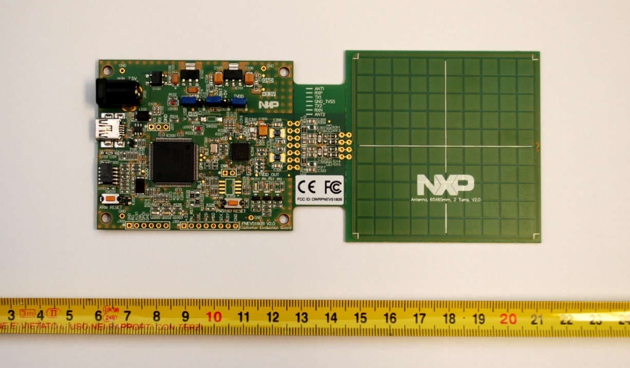
OWRPNEV5180B
Dec 23, 2015PN8180 Customer Evaluation Board
Equipment Class
DXX - Part 15 Low Power Communication Device Transmitter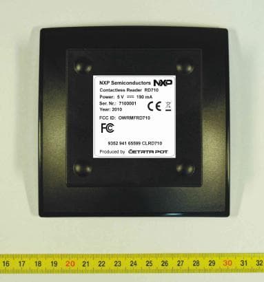
OWRMFRD710
May 09, 2011Contactless Reader
Equipment Class
DXX - Part 15 Low Power Communication Device Transmitter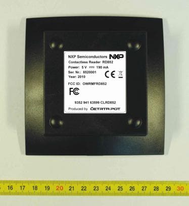
OWRMFRD852
May 09, 2011Contactless Reader
Equipment Class
DXX - Part 15 Low Power Communication Device Transmitter
OWR40089
Mar 21, 2002MIFARE Contactless Card Reader
Equipment Class
DXX - Part 15 Low Power Communication Device Transmitter
OWRICODE-SLEV900
Jul 09, 2000RFID Tag
Equipment Class
DXX - Part 15 Low Power Communication Device Transmitter