OWRPNEV5180BPN8180 Customer Evaluation Board
NXP Austria GmbH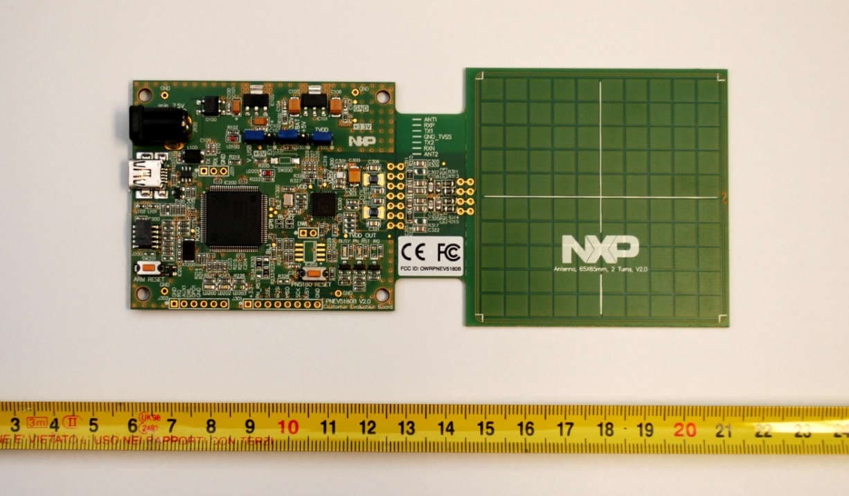
Click to zoom
Application Details
- Equipment Class
- DXX - Part 15 Low Power Communication Device Transmitter
- Date of Grant
- Dec 23, 2015
- Application Purpose
- Original Equipment
- Date of Application
- Dec 23, 2015
- Equipment Note
- PN8180 Customer Evaluation Board
- Frequency Range
- 13.56000000 - 13.56000000
- Company
- NXP Austria GmbH
- Country
- Austria
Documents & Files
Document Text
Text extracted from the exhibit documents filed with the FCC. Open a document above to read the original.
Users Manual
Document information InfoContent AuthorPavel Slamnik Author RoleDesign Engineer KeywordsCustomer Development Board PNEV5180B, RFID, NFC, Hardware Manual: Customer Development Board PNEV5180B Doc Rev 1.00 Approved — 2015.11.13 BL ID BL ID Hardware Manual Project Name: Integration Manual Project ID: 62743 Revision History RevisionDateDescriptionAuthor 1.02015.11.13First VersionPavel Slamnik SRS Template_vs 1.0public© NXP B.V. 2015. All rights reserved Doc ID: DOC-XXXXXXDoc Rev 1.00 Approved — 2015.11.132 of 16 Copyright: @2009, NXP Semiconductors The information contained herein is the exclusive and confidential property of NXP Semiconductors and, except as otherwise indicated, shall not be disclosed or reproduced in whole or in part. BL ID Hardware Manual Project Name: Integration Manual Project ID: 62743 Contents SRSt Template 1.0public© NXP B.V. 2015. All rights reserved Doc ID: DOC-XXXXXXDoc Rev 1.00 Approved — 2015.11.133 of 16 BL ID Hardware Manual Project Name: Integration Manual Project ID: 62743 STS Template 1.0public© NXP B.V. 2015. All rights reserved Doc ID: DOC-XXXXXXDoc Rev 1.00 Preliminary — 2015.11.134 of 16 BL ID Hardware Manual Project Name: Integration Manual Project ID: 62743 1.Customer Evaluation Board PNEV5180B: Photo Figure 1: Customer Evaluation Board PNEV5180B – side view. Figure 2: Customer Evaluation Board PNEV5180B – top view. STS Template 1.0public© NXP B.V. 2015. All rights reserved Doc ID: DOC-XXXXXXDoc Rev 1.00 Preliminary — 2015.11.135 of 16 BL ID Hardware Manual Project Name: Integration Manual Project ID: 62743 2.Customer Evaluation Board PNEV5180B: Description 1.Operational desription Customer Evaluation Board PNEV5180B is an example of implementation of ISO/IEC 14443A and ISO/IEC 14443B reader/writer, NFC reader/writer and Card Emulation Device on the same printed board. Middle size antenna, implemented on the same pcb (reader and antenna can be broken into separate parts), permits reading/writing on distance up to 50 mm (RFID card or other NFC device). The onboard USB connector permits direct connection and communication with personal computer. Power supply is via usb port or via external power supply (7.5 V / 500 mA). On the Customer Evaluation Board PNEV5180B main parts are easily visible: •the pcb antenna (can be separated from matching part), •the antenna matching components (can be separated from reader and antenna part), •the reader part: PN5180 reader IC, LPC 1769 microcontroller IC, two crystall oscillators and decopling capacitors, power supply ICs and EEPROM, USB serial communication port and JTAG port. The Customer Evaluation Board PNEV5180B uses USB serial communiation port for communicating with personal computer and transfer data. JTAG port is for development purposes (programming). Some test pins are added on pcb. The Customer Evaluation Board PNEV5180B has following features: •Supports ISO/IEC 14443A and ISO/IEC 14443B reader/writer up to 848 Kbps. •Supports MIFARE 1K/4K encryption in reader/writer mode. •Supports contactless RF communication according to the FeliCa protocol at 212 Kbps and 424 Kbps. •Supports all NFCIP-1 modes up to 424 Kbps. The PN512 handles the complete NFC framing and error detection. •Supports the reading of NFC Forum Tag Types 1,2,3,4,5 •P2P supported for types: A (106 kbit/s), F (212, 424 kbit/s) •ISO/IEC15693 reader (I-Code) •ISO/IEC 18000 EPC-HF reader (I-Code ILT) •EMVCo 2.4 L1 digital & analog Compliance •Card Emulation: ISO/IEC 14443A (up to 848 kbit/s) •Serial communication via USB port with Personal computer •Power supply via USB port or via external power adapter. Disclaimer : This module is intended only for development and evaluation purposes, and cannot be used in a finished product. STS Template 1.0public© NXP B.V. 2015. All rights reserved Doc ID: DOC-XXXXXXDoc Rev 1.00 Preliminary — 2015.11.136 of 16 BL ID Hardware Manual Project Name: Integration Manual Project ID: 62743 Figure 3: Customer Evaluation Board PNEV5180B - Block diagram. STS Template 1.0public© NXP B.V. 2015. All rights reserved Doc ID: DOC-XXXXXXDoc Rev 1.00 Preliminary — 2015.11.137 of 16 BL ID Hardware Manual Project Name: Integration Manual Project ID: 62743 Figure 4: Customer Evaluation Board PNEV5180B: dimensions, pcb with elements. STS Template 1.0public© NXP B.V. 2015. All rights reserved Doc ID: DOC-XXXXXXDoc Rev 1.00 Preliminary — 2015.11.138 of 16 BL ID Hardware Manual Project Name: Integration Manual Project ID: 62743 3. Customer Evaluation Board PNEV5180B: SPECIFICATION 3.1.Customer Evaluation Board PNEV5180B: Specifications Table 2: Customer Evaluation Board PNEV5180B – specifications Antenna PCB type, 65 mm x 65 mm Contactless operating frequency 13.56 MHz Card reading/writing distance Up to 50 mm Contactless (RFID) Smart Card Interface Reader/Writer mode ISO 14443 A up to 848 Kbps transmission rate (depending on card) ISO 14443 B up to 848 Kbps transmission rate (depending on card) Reader/Writer mode supporting JIS X 6319-4 (comparable with FeliCa scheme) NFC Forum tag type 1,2,3,4,5 reader NFC Forum compliance for R/W – Analog & Digital SO/IEC15693 reader (I-Code) ISO/IEC 18000 EPC-HF reader (I-Code ILT) EMVCo 2.4 L1 digital & analog Compliance Peer to Peer mode Passive-Initiator / Passive-Target Active-Initiator / Active-Target P2P supported for types: A (106 kbit/s), F (212,424 kbit/s) Card Emulation SO/IEC 14443A (up to 848 kbit/s) Microcontroller LPC1769 ARM Cortex-M3 based microcontroller with 512 kb internal flash memory, 64 kb internal RAM Clock Crystals 12.000 MHz crystal for CPU Firmware Customer developed firmware for testing PN5180 functionality Host Interface Host InterfaceUSB 2.0 (also supported USB 1.1) Transmission Speed12 Mbps (USB 2.0 full speed) Power Supply Bus powered Other Communication Interfaces JTAG IEEE1149.1 Serial Interface JTAG 10-pin connector; to connect JTAG adapter STS Template 1.0public© NXP B.V. 2015. All rights reserved Doc ID: DOC-XXXXXXDoc Rev 1.00 Preliminary — 2015.11.139 of 16 BL…
Text truncated - open the document above for the full version.
Block Diagram
NXP Austria GmbH Customer Development Board PNEV5180B Appendix B EUT Block Diagram Page 1 of 1 NXP Semiconductors GmbH © NXP B.V. 2013. For more information, visit: http://www.nxp.com Appendix B: Customer Development Board PNEV5180B – Block Diagram Picture 1: Customer Development Board PNEV5180B - Block Diagram
External Photos
NXP Austria GmbH Customer Development Board PNEV5180B Appendix A EUT Photo Page 1 of 1 NXP Semiconductors GmbH © NXP B.V. 2013. For more information, visit: http://www.nxp.com 1. Appendix A: Customer Development Board PNEV5180B – Photo Picture 1: Customer Development Board PNEV5180B - top view. Picture 2: Customer Development Board PNEV5180B - bottom view.
ID Label/Location Info
NXP Austria GmbH Customer Development Board PNEV5180B Appendix D EUT Labels Page 1 of 1 NXP Semiconductors GmbH © NXP B.V. 2013. For more information, visit: http://www.nxp.com
Internal Photos
NXP Austria GmbH Customer Development Board PNEV5180B Appendix A EUT Photo Page 1 of 1 NXP Semiconductors GmbH © NXP B.V. 2013. For more information, visit: http://www.nxp.com 1. Appendix A: Customer Development Board PNEV5180B – Photo Picture 1: Customer Development Board PNEV5180B - top view. Picture 2: Customer Development Board PNEV5180B - bottom view.
Operational Description
NXP Austria GmbH Customer Development Board PNEV5180B Appendix C EUT Photo Page 1 of 1 NXP Semiconductors GmbH © NXP B.V. 2013. For more information, visit: http://www.nxp.com Appendix C: Oscillator and PLL Frequencies Oscillator: - Microcontroller LPC 1769: 12 MHz (Quartz) - Reader IC PN5180: 27.12 MHz (Quartz) - Antenna Frequency (receiver): 13.56 MHz PLL – Frequencies: none.
Operational Description
PNEV5180B - Operational Description Customer Development Board PNEV5180B is an example of implementation of ISO/IEC 14443A and ISO/IEC 14443B reader/writer, NFC reader/writer and Card Emulation Device on the same printed board. Middle size antenna, implemented on the same pcb (reader and antenna can be broken into separate parts), permits reading/writing on distance up to 50 mm (RFID card or other NFC device). The onboard USB connector permits direct connection and communication with personal computer. Power supply is via usb port or via external power supply (7.5 V / 500 mA). Customer Evaluation Board PNEV5180B is intended to send and receive data according to the ISO 14443A and ISO 14443B protocol. Data transfer from reader to/from contactless cards operates at frequency 13.56 MHz. Data transfer between PN5180 reader IC and microcontroller LPC1769 is via SPI serial communication. LPC1769 microcontroller is connected to PN5180 Redaer IC via SPI serial communiaction port. JTAG connector is needed only to connect computer to write firmware into LPC1769 microcontroller. I2C interface on microcontroller is connected to EEPROM IC. SPI serial communication port on LPC1769 is used to communicate with PN5180 reader IC. Main part of Customer Evaluation Board PNEV5180B is contactless reader IC PN5180. The PN5180 is a highly integrated high power output NFC frontend IC for contactless communication at 13,56 MHz. This frontend IC utilizes an outstanding modulation and demodulation concept completely integrated for different kinds of contactless communication methods and protocols at 13.56 MHz. Contactless Reader IC PN5180 use only one power supply voltage: 3V3 V DC via power supply IC (LT1129CST- 3.3). All other voltages are generated internally. PN5180 IC use external quartz (27.12 MHz). SPI comunication is used to connect reader IC PN5180 to microcontroller. Complementary output stage (TX1, TX2) pins are used to generate output signal for antenna via filter stage and matching capacitors. Filter stage provide maximum adaption from output stage (PN5180) to antenna (with matching capacitors). Disclaimer: This module is intended only for development and evaluation purposes, and cannot be used in a finished product without further certification on the assembly.
Parts List/Tune Up Info
Customer Development Board PNEV5180B: Tune-UP Info Customer Development Board PNEV5180B contains reader IC PN5180 with RFID transmitter. RFID transmitter has fixed frequency (13,56 MHz). Transmitter part is optimal tuned to pcb antena via matching capacitors. The end user cannot change transmitter parameters (matching capacitors and antenna parameters). All matching capacitors are fixed – additional antenna tuning is not possible.
Parts List/Tune Up Info
PNEV5180B V2.0 Arrangement: Gregor Vrhovnik (16.10.2015) Component Label Value Manufacturer Footprint Ref Des Quan tity connector Micro USB-B 62910513682110104111-0001LF Micro-B W uerth Elektronik FCI SMD (Micro-B) J103 1 connector Mini USB-B 05481905725075BMR-05-SM-CR Mini-B Molex Neltron SMD (Mini-B) J102 1 quartz crystal 7M-27.120MEEQ-TQ027120032M10a 27.12MHz TXC CORPORATION SMI 4-SMD (3,2 x 2,5mm) XT300 1 quartz crystal NX5032GA-12.000000MHZ 12MHz NDK 2-SMD XT 200 1 IC – reader PN5180 NXP HVQFN40 IC300 1 IC – uP LPC1769FBD100 NXP 100-LQFP IC200 1 IC – REG (LDO) LT1129CST-5LT1129IST-5 5V / 0,7A Linear Technology SOT-223-3 IC100 1 IC – REG (LDO) LM3940IMP-3.3 3.3V / 1A National Semico nductor SOT-223-3 IC101 1 IC – Reset MAX811TEUS+TMIC811TUYADM811TARTZ Maxim Micrel Analog Devices SOT-143B IC201 1 inductor – ferrite bead BLM18PG181SN1 180R at 100MHz; 1,5A Murata INDC0603 L101, L102 2 inductor LQW 2BHN22NJ03L 22nH Murata INDC0805 L300 1 inductor PM1812-R10K-RCCM453232-R10MLCT 100nH Bourns INDC1812 L100 1 inductor 36502AR47JTDG 470nH / 220mA TE Connectivity IN DC0805 L301, L302 2 connector – PW R JACK PJ-202A 2,1 x 5,5mm CUI Inc. THT J1 00 1 transistor NPN BC817 45V/0.5A NXP SOT-23 T300, T301, T30 2 3 transistor PNP BC807 45V/0.5A NXP SOT-23 T100 1 diode (bridge) CDBHM240L 40V/2A Comchip Technology 4-SM D (MBS-2) D100 1 diode - ESD IP4220CZ6 NXP SOT-457 D101 1 button (switch) DTSM-32S-B Multicomp SMD SW 201, SW 300 2 pinheader – JTAG 20021121-00010C4LFFTS-105-01-L-DV 2x5 PIN (M) FCI Samtec SMD (R=1,27mm) J200 1 connector pinheader 1x2 PIN (M) R=2,54 Neltron THT J300 1 connector pinheader 1x3 PIN (M) R=2,54 Neltron THT J101, J303 2 LED KP-1608ID RED Kingbright SMD – 0603 LD100, LD201 2 LED KP-1608SGD GREEN Kingbright SMD – 0603 LD203, LD302 2 LED KPG-1608SEKC-T ORANGE Kingbright SMD – 0603 LD200, LD300 2 LED KP-1608QBC-D BLUE Kingbright SMD – 0603 LD202, LD301 2 cap. tantalum 10uF/16V CASE-A C101, C102 2 cap. tantalum 33uF/10V CASE-B C105, C106 2 cap. tantalum 100uF/10V CASE-B C300 1 capacitor 100nF CAPC0402 C205, C206, C207, C208, C209, C210, C211, C212, C213, C325, C329, C330 12 capacitor 15pF CAPC0603 C201, C202, C203, C204, C323, C324 6 capacitor 100nF CAPC0603 C100, C103, C104, C107, C110, C200, C214, C301, C303, C304, C309, C326, C328, C332 14 capacitor 470nF CAPC0603 C319 1 capacitor 1uF CAPC0603 C108, C109, C327 3 capacitor 4.7uF CAPC0603 C331 1 capacitor 6.8uF CAPC0603 C302 1 capacitor 15pF NP0 CAPC0805 C307, C320 2 capacitor 18pF NP0 CAPC0805 C308, C318 2 capacitor 33pF NP0 CAPC0805 C311, C315 2 capacitor 82pF NP0 CAPC0805 C305, C313, C317, C322 4 capacitor 120pF NP0 CAPC0805 C312, C316 2 capacitor 220pF NP0 CAPC0805 C310, C314 2 capacitor 1nF NP0 CAPC0805 C306, C321 2 resistor 0R RESC0402 R239, R240, R241, R242 4 resistor 0R RESC0603 R100, R101, R218, R229, R231, R319, R320, R325, R326, R327 10 resistor 33R RESC0603 R215, R217 2 resistor 330R RESC0603 R226, R306 2 resistor 1k RESC0603 R206, R210, R212, R221, R222, R223, R300, R301, R303, R304, R307 11 resistor 1k5 RESC0603 R103, R105, R213, R214, R227, R228 6 resistor 2k2 RESC0603 R102 1 resistor 2k7 RESC0603 R207, R312 2 resistor 3k3 RESC0603 R208, R220 2 resistor 4k7 RESC0603 R302, R305, R308 3 resistor 10k RESC0603 R104, R200, R201, R202, R203, R204, R205, R209, R219, R224, R225, R230 12 resistor 0R RESC0805 R233, R235 2 resistor 2R2 1% RESC0805 R311, R313, R314, R315 4 resistor 4k7 1% RESC0805 R310, R316 2 Do Not Place (DNP):IC – I2C EEPROM CAT24C128 DNP ON Semiconductor 8-SOIC IC202 1 button (switch) DTSM-32S-B DNP Multicomp SMD SW 200 1 connector pinheader 1x2 PIN (M) R=2,54 Neltron THT J304 1 connector pinheader 1x3 PIN (M) R=2,54 Neltron THT J201 1 connector pinheader 1x6 PIN (M) R=2,54 Neltron THT J302 1 connector pinheader 1x8 PIN (M) R=2,54 Neltron THT J301 1 resistor TBD DNP RESC0603 R211, R321, R322, R323, R324, R328 6 resistor 0R DNP RESC0603 R216, R238, R318 3 resistor 10k DNP RESC0603 R236, R237 2 resistor TBD DNP RESC0805 R309, R317 2 resistor 0R DNP RESC0805 R232, R234 2
Schematics
1 1 2 2 3 3 4 4 5 5 6 6 7 7 8 8 DD CC BB AA Title: Date: File: Revision: Drawn By: Sheet:of Paper Size:A3 Power Supply.SchDoc 15.9.2015 GVR 31 PNEV5180B 2.0 CDBHM240L AC 2 AC 1 V+ 3 V- 4 D100 100nF C100 100nF C103 LT1129CST-5 VIN 1 2 VOUT 3 GND 4 GND IC100 GND 1 2 3 PWR_DC J100 +5V POWER SUPPLY +5V K100 10uF/16V C101 10uF/16V C102 +5V MIN. +7.5V default VUSB 2k2 R102 RED PWR LD100 GND USB INTERFACE GND 180R at 100MHz L101 GND USB_N USB_P USB_VBUS 4 1 3 5 26 9 7 8 J102 MINI USB-B 100nH L100 GNDGND 100nF C110 GND 1uF C108 1uF C109 1 2 3 J101 3pin JMP ES3 4 ES4 6 Vp 5 ES2 3 ES1 1 GND 2 D101 IP4220CZ6 4 1 3 5 26 9 7 8 J103 MICRO USB-B GND 180R at 100MHz L102 GND GND 100nF C104 100nF C107 33uF/10V C105 LM3940IMP-3.3 VIN 1 2 VOUT 3 GND 4 GND IC101 GND 33uF/10V C106 +3.3V POWER SUPPLY GND K102 +3.3V +3.3V K101 power supply jumper 0R R100 0R R101 USB_CON 1k5 R105 1k5 R103 T100 BC807 10k R104 +3.3V GND GND GND GND GND GND TEST POINTS +3.3VREG PIC10001 PIC10002 COC100 PIC10101 PIC10102 COC101 PIC10201 PIC10202 COC102 PIC10301 PIC10302 COC103 PIC10401 PIC10402 COC104 PIC10501 PIC10502 COC105 PIC10601 PIC10602 COC106 PIC10701 PIC10702 COC107 PIC10801 PIC10802 COC108 PIC10901 PIC10902 COC109 PIC11001 PIC11002 COC110 PID10001 PID10002PID10003 PID10004 COD100 PID10101 PID10102 PID10103PID10104 PID10105 PID10106 COD101 PIIC10001 PIIC10002 PIIC10003 PIIC10004 COIC100 PIIC10101 PIIC10102 PIIC10103 PIIC10104 COIC101 PIJ10001 PIJ10002 PIJ10003 COJ100 PIJ10101 PIJ10102 PIJ10103 COJ101 PIJ10201 PIJ10202 PIJ10203 PIJ10204 PIJ10205 PIJ10206 PIJ10207 PIJ10208 PIJ10209 COJ102 PIJ10301 PIJ10302 PIJ10303 PIJ10304 PIJ10305 PIJ10306 PIJ10307 PIJ10308 PIJ10309 COJ103 PIK10001 COK100 PIK10101 COK101 PIK10201 COK102 PIK10301 COK103 PIK10401 COK104 PIK10501 COK105 PIK10601 COK106 PIL10001PIL10002 COL100 PIL10101PIL10102 COL101 PIL10201PIL10202 COL102 PILD10001 PILD10002 COLD100 PIR10001PIR10002 COR100 PIR10101PIR10102 COR101 PIR10201 PIR10202 COR102 PIR10301 PIR10302 COR103 PIR10401PIR10402 COR104 PIR10501PIR10502 COR105 PIT10001 PIT10002 PIT10003 COT100 PIK10101PIR10101 PIR10402 PIT10002 PIC10601 PIC10701 PIIC10103PIR10102PIJ10102 PIK10001 PIR10002 PIR10202 PIC10002 PIC10102PIC10202 PIC10302 PIC10402 PIC10502PIC10602 PIC10702 PIC10802PIC10902PIC11002 PID10004 PID10102 PIIC10002PIIC10004 PIIC10102PIIC10104 PIJ10205 PIJ10305 PIK10201 PIK10301 PIK10401 PIK10501 PIK10601 PIL10101 PIL10201 PILD10001 PIC10001 PIC10101 PID10003 PIIC10001 PIC10201 PIC10301 PIIC10003 PIJ10101 PIC10401 PIC10501 PIIC10101PIR10001 PIC10901PIC11001 PIJ10103 PIL10002 PID10001PIJ10001 PID10002PIJ10002 PIJ10003 PID10103PID10104 PIJ10204 PIJ10206 PIJ10207 PIJ10208 PIJ10209 PIL10102 PIJ10304 PIJ10306 PIJ10307 PIJ10308 PIJ10309 PIL10202 PILD10002 PIR10201 PIR10302 PIT10003 PIR10401PIR10502 PIT10001 PIR10501 NLUSB0CON PID10106 PIJ10202 PIJ10302 NLUSB0N PID10101 PIJ10203 PIJ10303 PIR10301 NLUSB0P PIC10801 PID10105 PIJ10201 PIJ10301 PIL10001 NLUSB0VBUS 1 1 2 2 3 3 4 4 5 5 6 6 7 7 8 8 DD CC BB AA Title: Date: File: Revision: Drawn By: Sheet:of Paper Size:A3 Processor.SchDoc 15.9.2015 GVR 32 PNEV5180B 2.0 P1.9/ENET_RXD0 91 P1.1/ENET_TXD1 94 P0.30/USB_D- 30 P0.21/RI1/RD1 57 P0.3/RXD0/AD0.6 99 P2.7/RD2/RTS1 66 P1.16/ENET_MDC 87 P1.0/ENET_TXD0 95 P1.8/ENET_CRS 92 P0.22/RTS1/TD1 56 P0.20/DTR1/SCL1 58 P0.10/TXD2/SDA2 48 P0.1/TD1/RXD3/SCL1 47 P2.8/TD2/TXD2 65 P0.29/USB_D+ 29 P0.2/TXD0/AD0.7 98 P2.13/EINT3/I2STX_SDA 50 P2.10/EINT0/NMI 53 NC 13 VSS 83 VSS 41 VDD 96 VDD 28 VDDREG 42 RTCX1 16 TRST 4 TDO/SWO 1 P4.28/RX_MCLK/TXD3 82 P3.25/MAT0.0/PWM1.2 27 P2.9/USB_CON/RXD2 64 P2.6/PCAP1.0/RI1 67 P2.3/PWM1.4/DCD1 70 P2.0/PWM1.1/TXD1 75 P1.30/VBUS/AD0.4 21 P1.27/CLKOUT/USB_OVRCR 43 P1.24/MCI2/PWM1.5/MOSI0 38 P1.21/MCABORT/PWM1.3/SSEL0 35 P1.18/USB_UP_LED/PWM1.1 32 P1.15/ENET_REF_CLK 88 P0.27/SDA0/USB_SDA 25 P0.24/AD0.1/I2SRX_WS 8 P0.18/DCD1/MOSI0 60 P0.15/TXD1/SCK0/SCK 62 P0.9/I2STX_SDA/MOSI1 76 P0.6/I2SRX_SDA/SSEL1 79 P0.0/RD1/TXD3/SDA1 46 VSSA 11 VSS 72 VSS 97 VSS 55 P2.11/EINT1/I2STX_CLK 52 VREF+ 12 VDD 71 VREF- 15 VDD 54 VDDREG 84 VDDA 10 VBAT 19 RTCX2 18 XTAL2 23 XTAL1 22 P4.29/TX_MCLK/RXD3 85 TDI 2 TMS/SWDIO 3 TCK/SWDCLK 5 RTCK 100 RSTOUT 14 P3.26/STCLK/PWM1.3 26 P2.4/PWM1.5/DSR1 69 P2.1/PWM1.2/RXD1 74 P1.31/SCK1/AD0.5 20 P2.2/PWM1.3/CTS1 73 P2.5/PWM1.6/DTR1 68 P1.28/MCOA2/PCAP1.0 44 P1.25/MCOA1/MAT1.1 39 P1.22/MCOB0/USB_PWRD 36 P1.19/MCOA0/USB_PWR 33 P1.20/MCI0/PWM1.2 34 P1.23/MCI1/PWM1.4/MISO0 37 P1.26/MCOB1/PWM1.6 40 P1.10/ENET_RXD1 90 P1.4/ENET_TX_EN 93 P1.14/ENET_RX_ER 89 P0.28/SCL0/USB_SCL 24 P0.25/AD0.2/I2SRX_SDA/TXD3 7 P0.19/DSR1/SDA1 59 P0.23/AD0.0/I2SRX_CLK 9 P0.26/AD0.3/RXD3 6 P0.16/RXD1/SSEL0 63 P0.7/I2STX_CLK/SCK1 78 P0.4/I2SRX_CLK/RD2 81 P0.5/I2SRX_WS/TD2 80 P0.8/I2STX_WS/MISO1 77 P0.11/RXD2/SCL2 49 VSS 31 P2.12/EINT2/I2STX_WS 51 RESET 17 P1.29/MCOB2/PCAP1.1 45 P1.17/ENET_MDIO 86 P0.17/CTS1/MISO0 61 IC200 LPC1769FBD100 GND 100nFC206 100nFC207 100nFC208 100nFC209 100nFC210 100nFC211 100nFC212 100nFC213 GND +3.3V 100nFC205 GND 10kR224 +3.3V 0RR218 +3.3V 15pFC202 15pFC201 12MHz XT200 GND GND +3.3V 100nF C200 GND TCK TDI TMS TDO RST 10k R200 10k R201 10k R202 JTAG INTERFACE 10k R203 RTCK 1k R206 MR 3 VDD 4 GND 1 RES 2 IC201 MAX811 GND +3.3V GND 0R DNP R216 TDO TDI TMS TCK RTCK RST LED_G LED_B LED_O LED_R 1k R221 1k R222 ORANGELD200 REDLD201 470R R223 BLUELD202 1k R226 GREENLD203 GND LED_R STATUS LEDS LED_O LED_G LED_B TXD0 RXD0 1 2 3 DNPLPC INIT J201 GND TXD0 RXD0 10k R219 +3.3V SCK SSEL MISO MOSI SDA SCL 100nF C214 GND +3.3V 10k R230 0R R231 GND 10k R225 0R R229 GND +3.3V GND +3.3V SDA 5 A1 2 VCC 8 GND 4 A0 1 WP 7 A2 3 SCL 6 DNP 24C128 IC202 SERIAL EEPROM 1k5 R227 +3.3V 1k5 R228 SDA SCL USB_N USB_P 33RR215 33RR217 15pF C204 USB_CON 15pF C203 GND JTAG_HEADER_50mil 10 7 4 1 9 6 3 8 5 2 J200 FTS-105-01-L-DV 1k5R213 +3.3V 1k5R214 TBD DNP R211 ARM RESET 1 2 SW201 10kR204 +3.3V LPC_OSC PN_RST K200 AD4 3k3R220 GND 2k7R207 AUX2_DWL AD0 AD1 AD0 AD1 AD4 1kR210 1kR212 3k3R208 10kR209 +3.3V GND GND GND BL2 W DOFF K202 K203 K201 BL1 GPI1 K204 BL2 10kR205 +3.3V DNP 12 SW…
Text truncated - open the document above for the full version.
Test Report
T251-0909/15 Page: 2 (66) CONTENTS page 1 GENERAL 3 1.1 EQUIPMENT UNDER TEST 3 1.2 ANSI C63.4 SUBPART SELECTION 4 1.3 CLASS STATEMENT REQUIREMENTS 4 1.4 LIST OF MEASUREMENTS PERFORMED 4 1.5 OCCUPIED BANDWIDTH MEASUREMENT 4 1.6 QUASI-PEAK DETECTOR 4 1.7 PEAK, RMS, AND AVERAGE DETECTORS 4 2 LIMITS FOR ALL SUBPARTS 5 2.1 SUBPART C: INTENTIONAL RADIATORS 5 3 ALL TEST EQUIPMENT AND THEIR DESCRIPTION 7 3.1 GENERAL INFORMATION 7 4 CONVERSION FACTORS AND ALL OTHER FORMULAS 8 5 GENERAL AND SPECIAL CONDITIONS DESCRIPTION 9 5.1 GENERAL CONDITION DESCRIPTION 9 5.2 SPECIAL CONDITION DESCRIPTION 12 6 TEST SUMMARY 13 6.1 OPERATING VOLTAGES/FREQUENCIES USED FOR TESTING 13 7 EMISSION TESTS 14 7.1 CONDUCTED EMISSION MEASUREMENT (INTENTIONAL RADIATOR) 14 7.2 RADIATED EMISSION MEASUREMENT (INTENTIONAL RADIATOR) 32 7.3 BANDWIDTH OF THE EMISSION (INTENTIONAL RADIATOR) 53 7.4 SPECTRUM MASK (INTENTIONAL RADIATOR) 58 7.5 FREQUENCY TOLERANCE OF THE CARRIER SIGNAL 64 T251-0909/15 Page: 3 (66) 1 GENERAL History sheet Date Report No. Change Revision 2015-12-16 T251-0909/15 Initial Test Report issued. -- Environmental conditions: Ambient temperature: 15°C to 35°C Relative humidity: 30% to 60% Atmospheric pressure: 860 mbar to 1060 mbar 1.1 Equipment under test Customer Evaluation Board Type: PNEV5180B FCC ID: OWRPNEV5180B 1.1.1 General product information Tested sample number: S20156422 (Antenna Board 65 x 65 mm), Measurements done with HP EliteBook 8560p and NPX_PN518_SupportTool_v1_7 software. Picture of EUT T251-0909/15 Page: 4 (66) Corrected page: 2015-12-23 1.2 ANSI C63.4 Subpart selection Subpart C: Intentional Radiators Section 15.203: Antenna Requirement PNEV5180B has permanently attached antenna and can not be replaced. 1.3 Class statement requirements • The Class A statement cautions that operation of the device in a residential area is likely to cause harmful interference. • The Class B statement offers several suggestions for minimizing interference to radio or TV receivers, including reorienting the receiving antenna and moving the Class B device farther away from the receiver. 1.4 List of measurements performed PART 15 section Test name 15.207 Conducted emission 15.209 Radiated emission 15.215 Bandwidth of the emission 15.225 Radiated emission 1.5 Occupied bandwidth measurement Fundamental frequency Minimum resolution bandwidth 9 kHz to 30 MHz 1 kHz 30 to 1000 MHz 10 kHz 1000 MHz to 40 GHz 100 kHz 1.6 Quasi-peak detector Frequency range Bandwidth (-6dB) 10 Hz to 20 kHz Full range (wideband) 10 kHz to 150 kHz 200 Hz 150 kHz to 30 MHz 9 kHz 30 MHz to 1 GHz 120 kHz 1.7 Peak, rms, and average detectors Frequency range Bandwidth (-6dB) 10 Hz to 20 kHz 10, 100, 1000 Hz 10 kHz to 150 kHz 1 and 10 kHz 150 kHz to 30 MHz 1 and 10 kHz 30 MHz to 1 GHz 10 and 100 kHz 1 GHz to 40 GHz 0.1, 1.0 and 10 MHz T251-0909/15 Page: 5 (66) 2 LIMITS FOR ALL SUBPARTS 2.1 Subpart C: Intentional Radiators 2.1.1 Conducted emission limits: Limits: Limits (dBμV) Frequency Range (MHz) Quasi-peak Average 0.15 to 0.5 66 – 56* 56 – 46* 0.5 to 5.0 56 46 5.0 to 30.0 60 50 * Decreases with the logarithm of the frequency. The shown limits in table shall not apply to carrier current systems operating as intentional radiators on frequencies below 30 MHz. In lieu thereof, these carrier current systems shall be subject to the following standards: • For carrier current systems containing their fundamental emission within the frequency band 535-1705 kHz and intended to be received using a standard AM broadcast receiver: no limit on conducted emissions. • For all other carrier current systems: 1000 μV within the frequency band 535-1705 kHz, as measured using a 50 μH/50 ohms LISN. • Carrier current systems operating below 30 MHz are also subject to the radiated emission limits as appropriate. 2.1.2 Radiated emission limits: Limits: Limits (dBμV/m) Frequency Range (MHz) VERTICAL HORIZONTAL Test distance (m) 0,009 to 0,490 20*log(2400/F(kHz)) 20*log(2400/F(kHz))300 0,490 to 1,705 20*log(2400/F(kHz)) 20*log(2400/F(kHz))30 1,705 to 30,0 30 30 30 30 to 88 40** 40** 3 88 to 216 43.5** 43.5** 3 216 to 960 46** 46** 3 Above 960 54 54 3 ** Except as provided in paragraph below, fundamental emissions from intentional radiators operating under this section shall not be located in the frequency bands 54-72 MHz, 76-88 MHz, 174-216 MHz or 470-806 MHz. Perimeter protection systems may operate in the 54-72 MHz and 76-88 MHz bands under the provisions of this section. The use of such perimeter protection systems is limited to industrial, business and commercial applications. Additional FCC requirements per clause 15.215. Intentional radiators operating under the alternative provisions to the general emission limits must be designed to ensure that the 20 dB bandwidth of the emission, or whatever bandwidth may otherwise be specified in the specific rule section under which the equipment operates, is contained within the frequency band designated in the rule section under which the equipment is operated. T251-0909/15 Page: 6 (66) Additional FCC requirements per clause 15.225. Fundamental Frequency (MHz) Field strength of fundamental (μV/m) Test distance (m) 13.553-13.567 15,848 30 13.410-13.553 and 13.567-13.710 334 30 13.110-13.410 and 13.710-14.010 106 30 Outside band 13.110-14.010 As per clause 15.209 30 The frequency tolerance of the carrier signal shall be maintained within ±0.01% of the operating frequency over a temperature variation of −20 degrees to 50 degrees C at normal supply voltage, and for a variation in the primary supply voltage from 85% to 115% of the rated supply voltage at a temperature of 20 degrees C. For battery operated equipment, the equipment tests shall be performed using a new battery. T251-0909/15 Page: 7 (66) 3 ALL TEST EQUIPMENT AND THEIR DESCRIPTION 3.1 General information Description Model No. SIQ No. Last calibration Calibrated until Calibration period Used Rohde-Schwarz, RFI receiver ESU8 105187 2015-10 2017-10 24 months Rohde-Schwarz,…
Text truncated - open the document above for the full version.
Test Report
T251-0909/15 Page: 34 (66) 7.2.4 Test result (15.209) Preliminary measurement at 3 m in SAC: T251-0909/15 Page: 35 (66) T251-0909/15 Page: 36 (66) T251-0909/15 Page: 37 (66) T251-0909/15 Page: 38 (66) Final measurement at 10 m in OATS Results with measuring distance of 10 m Operating mode Frequency (MHz) Measured value (dBμV/m) Limit (dBμV/m) Margin (dB) Waiting for a tag 13,56 45,44 104,00 - 58,56 Reading a tag 13,56 35,67 104,00 - 68,33 Calculated value from 10 m to 30 m Operating mode Frequency (MHz) Measured value at 10 m (dBμV/m) Correction factor from 10 m to 30 m (dB) Calculated value at 30 m (dBμV/m) Limit at 30 m (dBμV/m) Margin (dB) Waiting for a tag 13,56 45,44 20 25,44 84,00 - 58,56 Reading a tag 13,56 35,67 20 15,67 84,00 - 68,33 NOTE: Antenna factor and cable loss are already included in measurement correction. T251-0909/15 Page: 39 (66) T251-0909/15 Page: 40 (66) T251-0909/15 Page: 41 (66) T251-0909/15 Page: 42 (66) T251-0909/15 Page: 43 (66) T251-0909/15 Page: 44 (66) T251-0909/15 Page: 45 (66) T251-0909/15 Page: 46 (66) T251-0909/15 Page: 47 (66) T251-0909/15 Page: 48 (66) T251-0909/15 Page: 49 (66) T251-0909/15 Page: 50 (66) T251-0909/15 Page: 51 (66) Worst case measurements: T251-0909/15 Page: 52 (66) T251-0909/15 Page: 53 (66) 7.3 Bandwidth of the emission (intentional radiator) Section 15.215 Additional provisions to the general radiated emission limitations 7.3.1 Test instruments Description & Manufacturer Model No. SIQ No. Last calibration Calibrated until Calibration period Used ETS, Anechoic chamber 3m 103949 2014-11 2016-11 24 months X Rohde-Schwarz, RFI receiver ESU26 106897 2014-01 2016-01 24 months X EMCO, Antenna 3142B 06/068 2015-09 2017-09 24 months Rohde & Schwarz, Active loop antenna HFH2-Z2 / 2015-09 2017-09 24 months X Heinrich Deisel, Turn table DS 420.00 103337 NA NA NA X ETS, Antenna tower / / NA NA NA X ETS, Controller for turn table and antenna tower / / NA NA NA X 7.3.2 Test procedure 1. The EUT was placed on the top of a rotating table 0.8 meters above the ground in an Anechoic Chamber. The table was rotated 360 degrees to determine the position of the highest radiation. 2. The EUT was set 3 m away from the interference-receiving antenna. 3. Resolution bandwidth is set to a value greater than 5% of the allowed bandwidth. If no bandwidth specifications are given, the guidelines in Section 1.4 are used 7.3.3 Test results Device passed the requirements stated in ANSI C63.4, FCC Part 15, Subpart C. T251-0909/15 Page: 54 (66) T251-0909/15 Page: 55 (66) T251-0909/15 Page: 56 (66) T251-0909/15 Page: 57 (66) Frequency (MHz) Permitted frequency band (MHz) 20 dB bandwidth (kHz) PASS/FAIL 13.56 13.110 – 14.010 2.64 PASS T251-0909/15 Page: 58 (66) 7.4 Spectrum mask (intentional radiator) Section 15.225 Operation within the band 13.110 – 14.010 MHz – clause a – clause d 7.4.1 Test instruments Description & Manufacturer Model No. SIQ No. Last calibration Calibrated until Calibration period Used ETS, Anechoic chamber 3m 103949 2014-11 2016-11 24 months X Rohde-Schwarz, RFI receiver ESU26 106897 2014-01 2016-01 24 months X EMCO, Antenna 3142B 06/068 2015-09 2017-09 24 months Rohde & Schwarz, Active loop antenna HFH2-Z2 / 2015-09 2017-09 24 months X Heinrich Deisel, Turn table DS 420.00 103337 NA NA NA X ETS, Antenna tower / / NA NA NA X ETS, Controller for turn table and antenna tower / / NA NA NA X 7.4.2 Test procedure 1. The EUT was placed on the top of a rotating table 0.8 meters above the ground in an Anechoic Chamber. The table was rotated 360 degrees to determine the position of the highest radiation. 2. The EUT was set 3 m away from the interference-receiving antenna. 3. F…
Text truncated - open the document above for the full version.
Contact Information
Applicant
Juergen Schroeder(Senior Product Manager)
Technical Contact
Test Firm
SIQ LjubljanaMarjan Mak
Technical Specifications
| # | Rule Parts | Frequency Range | Power Output |
|---|---|---|---|
| 1 | 15C | 13.56 MHz - 13.56 MHz | - |
Other Applications from NXP Austria GmbH

OWROM5569-NT322E
Dec 16, 2015NTAG I2C plus Explorer Kit
Equipment Class
DXX - Part 15 Low Power Communication Device Transmitter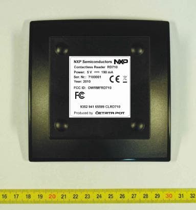
OWRMFRD710
May 09, 2011Contactless Reader
Equipment Class
DXX - Part 15 Low Power Communication Device Transmitter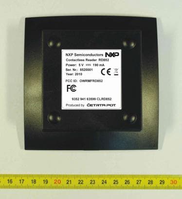
OWRMFRD852
May 09, 2011Contactless Reader
Equipment Class
DXX - Part 15 Low Power Communication Device Transmitter
OWR40089
Mar 21, 2002MIFARE Contactless Card Reader
Equipment Class
DXX - Part 15 Low Power Communication Device Transmitter
OWRICODE-SLEV900
Jul 09, 2000RFID Tag
Equipment Class
DXX - Part 15 Low Power Communication Device Transmitter