OXTLSE039PCMCIA Bluetooth Interface
National Semiconductor Sweden AB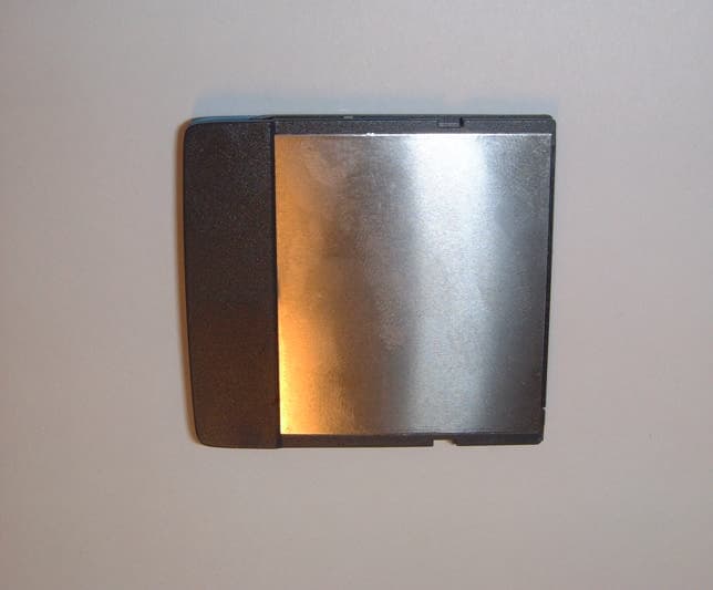
Click to zoom
Application Details
- Equipment Class
- DSS - Part 15 Spread Spectrum Transmitter
- Date of Grant
- Aug 08, 2001
- Application Purpose
- Original Equipment
- Date of Application
- Aug 08, 2001
- Equipment Note
- PCMCIA Bluetooth Interface
- Frequency Range
- 2402.00000000 - 2480.00000000
- Country
- Sweden
Documents & Files
Document Text
Text extracted from the exhibit documents filed with the FCC. Open a document above to read the original.
Users Manual
Users Manual LSE0391 (4) Uppgjord (även faktaansvarig om annan) - Prepared (also subject responsible if other)Nr - No. Mikael Ohlsson Dokansv/Godk - Doc respons/ApprovedKontr - CheckedDatum - DateRevFile 2001-04-20 1 REGULATIONS 1.1 EUROPEAN COMPLIANCE EMC, Electrical Safety and Radio EC Directive Compliance The CE mark is affixed to this product to confirm compliance with the following European Community Directives: • Council Directive 1999/5/EC of the European Parliament and the Council of 9 March 1999 on radio equipment and telecommunications terminal equipment and the mutual recognition of their conformity. • Council Directive 89/336/EEC of 3 May 1989 on the approximation of the laws of Member States relating to electromagnetic compatibility (EMC). • Council Directive 73/23/EEC of 19 february 1973 on the harmonization of the laws of Member States relating to electrical equipment designed for use within certain voltage limits. Each of the above mentioned directives amended by • Council Directive 93/68/EEC of 22 July 1993 on the harmonization of the CE marking requirements. A “Declaration of Conformity” in accordance with the relevant standards to confirm compliance with the above mentioned directives has been made and is on file at Wireless Solutions Sweden AB, Sundbyberg, Sweden. 1.2 FCC (US) COMPLIANCE FCC R.F. Interference Statement This device complies with Part 15 of the FCC rules. Operation is subject to the following two conditions: (1) This device may not cause harmful interference, and (2) This device must accept any interference received, including interference that may cause undesired operation. Users Manual LSE0392 (4) Uppgjord (även faktaansvarig om annan) - Prepared (also subject responsible if other)Nr - No. Mikael Ohlsson Dokansv/Godk - Doc respons/ApprovedKontr - CheckedDatum - DateRevFile 2001-04-20 This equipment has been tested and found to comply with the limits for class B Digital device, pursuant to part 15 of the FCC Rules. These limits are designed to provide reasonable protection against harmful interference in a residential installation. This equipment generates and can radiate radio frequency energy and, if not installed and used in accordance with the instructions, may cause harmful interference to radio communications. However, there is no guarantee that interference will not occur in a particular installation. If this equipment does cause harmful interference to radio or television reception, which can be determined by turning the equipment off and on, the user is encouraged to try to correct the interference by one or more of the following measures. • Reorient or relocate the receiving antenna • Increase the separation between the equipment and receiver • Connect the equipment into an outlet on a circuit different from that to which the receiver is connected • Consult the dealer or an experienced radio/TV technician for help Any changes or modifications not expressly approved by Wireless Solutions Sweden AB could void the user’s authority to operate the equipment. 1.3 EXPOSURE TO RADIO FREQUENCY RADIATION The radiated output power of the equipment is far below the FCC radio frequency exposure limits. Neverthless, it is advised to use the equipment in such a manner that the potential for human contact during normal operation is minimized. 1.4 IMPORTANT SAFETY INFORMATION 1.4.1 SAFETY WARNINGS ! Interference All wireless devices may get interference, which could affect performance. Switch off in aircraft Wireless devices can cause interference. Using them on aircraft is illegal. Switch off when refueling Do not use the wireless Compact Flash at a refueling point. Do not use near fuel or chemicals. Switch off near blasting Do not use the Compact Flash where blasting is in progress. Observe restrictions, and follow any regulations or rules. Users Manual LSE0393 (4) Uppgjord (även faktaansvarig om annan) - Prepared (also subject responsible if other)Nr - No. Mikael Ohlsson Dokansv/Godk - Doc respons/ApprovedKontr - CheckedDatum - DateRevFile 2001-04-20 Switch off near medical equipment. Follow all regulations and rules in hospitals. Do not use the Compact Flash near medical equipment. Use qualified service Only qualified service personnel must repair equipment. Accessories Use only approved accessories. Do not connect incompatible products. Connecting to other devices When connecting to any other device, read its user’s guide for detailed safety instructions. Do not connect incompatible products. Chemicals Do not store or use the Compact Flash in places where it may be exposed to chemicals or chemical vapors. Doing so will lead to fires or electric chocks. Prohibited areas Do not use the Compact Flash when the use of a Bluetooth application is prohibited or when it may cause interference or danger. Humid or dusty places Do not store or use the PrinteCompact Flash in humid or dusty places. Doing so could lead to fires or electric chocks. Do not disassemble or modify the Compact Flash in any way Do not disassemble or modify the Compact Flash in any way. Doing so without the express approval by the manufacturer will void user authority to operate the equipment and may lead to fires or electric shocks. Switch off near a microwave oven in use Do not use the Bluetooth application close to a microwave oven in use. There may be a risk that the system will be disturbed. Heat, direct sunlight Avoid installing the Compact Flash near sources of heat or in direct sunlight. Use only appropriate Region settings Use only the region setting appropriate for the area where the Bluetooth application is used at the present time. Using the LSE039 Compact Flash in any other region or with an incorrect region setting may be illegal. Connect only to SELV circuits Users Manual LSE0394 (4) Uppgjord (även faktaansvarig om annan) - Prepared (also subject responsible if other)Nr - No. Mikael Ohlsson Dokansv/Godk - Doc respons/ApprovedKontr - CheckedDatum - DateRevFile 2001-04-20 The Comp…
Text truncated - open the document above for the full version.
Attestation Statements
Hop Selection29 November 1999127 BLUETOOTH SPECIFICATION Version 1.0 Bpage 127 of 1082 Baseband Specification 11 HOP SELECTION In total, 10 types of hopping sequences are defined − five for the 79-hop and five for the 23-hop system, respectively. Using the notation of parentheses () for figures related to the 23-hop system, these sequences are: •A page hopping sequence with 32 (16) unique wake-up frequencies dis- tributed equally over the 79 (23) MHz, with a period length of 32 (16); •A page response sequence covering 32 (16) unique response frequencies that all are in an one-to-one correspondence to the current page hopping sequence. The master and slave use different rules to obtain the same sequence; •An inquiry sequence with 32 (16) unique wake-up frequencies distributed equally over the 79 (23) MHz, with a period length of 32 (16); •A inquiry response sequence covering 32 (16) unique response frequen- cies that all are in an one-to-one correspondence to the current inquiry hop- ping sequence. •A channel hopping sequence which has a very long period length, which does not show repetitive patterns over a short time interval, but which dis- tributes the hop frequencies equally over the 79 (23) MHz during a short time interval; For the page hopping sequence, it is important that we can easily shift the phase forward or backward, so we need a 1-1 mapping from a counter to the hop frequencies. For each case, both a hop sequence from master to slave and from slave to master are required. The inquiry and inquiry response sequences always utilizes the GIAC LAP as lower address part and the DCI (Section 5.4 on page 73) as upper address part in deriving the hopping sequence, even if it concerns a DIAC inquiry. 11.1 GENERAL SELECTION SCHEME The selection scheme consists of two parts: • selecting a sequence; • mapping this sequence on the hop frequencies; The general block diagram of the hop selection scheme is shown in Figure 11.1 on page 128. The mapping from the input to a particular hop frequency is per- formed in the selection box. Basically, the input is the native clock and the cur- rent address. In CONNECTION state, the native clock (CLKN) is modified by an offset to equal the master clock (CLK). Only the 27 MSBs of the clock are used. In the page and inquiry substates, all 28 bits of the clock are used. How- ever, in page substate the native clock will be modified to the master’s estimate of the paged unit. 12829 November 1999Hop Selection BLUETOOTH SPECIFICATION Version 1.0 Bpage 128 of 1082 Baseband Specification The address input consists of 28 bits, i.e., the entire LAP and the 4 LSBs of the UAP. In CONNECTION state, the address of the master is used. In page sub- state the address of the paged unit is used. When in inquiry substate, the UAP/LAP corresponding to the GIAC is used. The output constitutes a pseudo- random sequence, either covering 79 hop or 23 hops, depending on the state. Figure 11.1: General block diagram of hop selection scheme. For the 79-hop system, the selection scheme chooses a segment of 32 hop frequencies spanning about 64 MHz and visits these hops once in a random order. Next, a different 32-hop segment is chosen, etc. In case of the page, page scan, or page response substates, the same 32-hop segment is used all the time (the segment is selected by the address; different units will have dif- ferent paging segments). In connection state, the output constitutes a pseudo- random sequence that slides through the 79 hops or 23 hops, depending on the selected hop system. For the 23-hop systems, the segment size is 16. The principle is depicted in Figure 11.2 . Figure 11.2: Hop selection scheme in CONNECTION state. SELECTION BOX hop frequency UAP/LAP 23/79 mode CLOCK 27 28 04662642 781 737577 segment 1 segment 2 segment 3 ∆ Europe/US Japan/France/Spain 79 23 32 16 16 8 segment length# of hops ∆ Hop Selection29 November 1999129 BLUETOOTH SPECIFICATION Version 1.0 Bpage 129 of 1082 Baseband Specification 11.2 SELECTION KERNEL The hop selection kernels for the 79 hop system and the 23 hop system are shown in Figure 11.3 on page 129 and Figure 11.4 on page 129, respectively. The X input determines the phase in the 32-hop segment, whereas Y1 and Y2 selects between master-to-slave and slave-to-master transmission. The inputs A to D determine the ordering within the segment, the inputs E and F determine the mapping onto the hop frequencies. The kernel addresses a register containing the hop frequencies. This list should be created such that first all even hop fre- quencies are listed and then all odd hop frequencies. In this way, a 32-hop seg- ment spans about 64 MHz, whereas a 16-hop segment spans the entire 23-MHz. Figure 11.3: Block diagram of hop selection kernel for the 79-hop system. Figure 11.4: Block diagram of hop selection kernel for the 23-hop system. X O R XOR 55 XADD mod32 AB 4 5 5 5 ADD EF 7 7 7 0 2 4 CD 5 9 5 Y1 Y2 mod 79 1 78 3 77 PERM5 X O R XOR ADD AB 45 ADD EF 77 0 2 4 CD 5 9 5 Y1 Y2 X 4 mod16 mod 23 22 1 3 21 4445 PERM4 13029 November 1999Hop Selection BLUETOOTH SPECIFICATION Version 1.0 Bpage 130 of 1082 Baseband Specification The selection procedure consists of an addition, an XOR operation, a permuta- tion operation, an addition, and finally a register selection. In the remainder of this chapter, the notation A i is used for bit i of the BD_ADDR. 11.2.1 First addition operation The first addition operation only adds a constant to the phase and applies a modulo 32 or a modulo 16 operation. For the page hopping sequence, the first addition is redundant since it only changes the phase within the segment. How- ever, when different segments are concatenated (as in the channel hopping sequence), the first addition operation will have an impact on the resulting sequence. 11.2.2 XOR operation Let Z’ denote the output of the first addition. In the XOR operation, the four LSBs of Z’ are modulo-2 added to the address bits A 22-19 . The operation is illustrated…
Text truncated - open the document above for the full version.
Block Diagram
Block Diagram of the ROK 101 007 Ericsson Bluetooth Module (Grey part is the Radio module, PBA 313 01/ 2)
Cover Letter(s)
FCC Authorization Uppgjord (även faktaansvarig om annan) - Prepared (also subject responsible if other)Nr - No. WSS Mikael Ohlsson Dokansv/Godk - Doc respons/ApprovedKontr - CheckedDatum - DateRevFile 2001-04-26A Notes, FCC Authorization, LSE039 Compact Flash. 1. The Compact Flash, OXTLSE039, have to be seen as a modular approval, it is intended for laptop’s, PDA:s, desktop PC’s and other “type 1” compact flash host enabled devices to interface to Bluetooth. The Compact flash fulfills the criteria for modular approval (own RF-shielding, own power supply regulation, permanently affixed antenna, stand-alone test report, own FCC-label etc.) The Compact flash tested with a laptop computer and an external jigg as a platform must not be seen as a system. The Compact Flash is a unique product. For reference, see the already FCC-approved OXTLSE041 modular approved PC-card. 2. Block diagram is attached. The block diagram in the Ericsson description is separately attached. 3. According to the Ericsson data sheet, PBA 313 01/2, page 4, the 15.247 input bandwidth requirement is specified under RF-Specifications as “Double-sided IF Bandwidth” and equal with the input bandwidth (Spec. 1 MHz). The information received from Ericsson is that the PBA 313 01/2 Bluetooth Radio is an alternative to the FCC-approved Bluetooth module, FCC-identifier: CGK8001001, and will be FCC approved soon, with the above mentined Bluetooth module approval as basis. 4. Description of the antenna type for each device are provided in the Block diagram/Circuit Description. 5. Since the devices/marking labels are to small to place the required text according to part 15.19(a) (3),The information required by this paragraph is already placed in the users manual. This will be FCC accepted according to part 15.19(a) (5). The following text can be seen in the User’s Manual for OXTLSE019 and OXTLSE041: This device complies with Part 15 of the FCC rules. Operation is subject to the following two conditions: (1) this device may not cause harmful interference, and (2) this device must accept any interference received, including interference that may cause undesired operation. Mikael Ohlsson Product Certification Wireless Solutions Sweden AB Rissneleden 138, plan 6 S-174 02 Sundbyberg, Sweden Phone: +46 8 7337651 Mobile: +46 733 604044 E-mail: [email protected]
Cover Letter(s)
FCC ID: OXTLSE039 Part 15 Unlicensed Modular Transmitter Approval Justification per DA 00-1407, released: June 26, 2000 re quire me ntre fe re nce 1The modular transmitter must have its ow n RF shielding. Relevant emission requirements are met with metallic shielding shown on the Compact Flash for mat i n external photos . 2The mod ular trans mitter must have b uffered mod ulation/data i np uts All inputs to the modules are buffered through logic or microprocessor inputs. S e e sc he ma t ic d ia g ra ms . 3The modular transmitter must have its own pow er supply regulation. All power lines derived from the host device are regulated before energizing other circuits internal to the EUT. Se e sche matic diag ra m. 4The modular transmitter must comply with the antenna requirements of Section 15.203 and 15.204(c). The EUT has a built-in antenna, which is inaccessible to the user. See pro duct spe cificatio n and external photos .. 5The modular transmitter must be tested in a stand-alone configuration, i.e., the module must not be inside another device during testing. EUT was tested on a “Blueboy” open Bluetooth test bed which provides no shielding. See description in test re port and test setup photos . 6The modular transmitter must be labeled with its own FCC ID number, and, if the FCC ID is not visible when the module is installed inside another device, then the outside of the device into which the module is installed must also display a label referring to the enclosed mod ule. The EUT carries an FCC ID label whose artwork and label position are clearly indicated; see Label exhibit. The FCC ID is visible to the end user prior to installation, thereby satisfying the labeling requirement. 7The modular transmitter must comply with any specific rule or operating requirements applicable to the trans mi tter a nd the manufacturer must provide adequate instructions along with the module to explain any such requirements. A copy of these instructions must be included in the application for equipment authorization. The EUT incorporates a certified Bluetooth module FCC ID: CGK8001001, whose 15.247 spread spectrum frequency hopping functional parameters cannot be altered by the user. The EUT was tested at its ma xi mum da ta rate. Se e Blue tooth mo dule de scri ptio n . 8The modular transmitter must comply with any applicable RF exposure requirements. For example, FCC Rules in Sections 2.1091, 2.1093 and specific Sections of Part 15, including 15.319(i), 15.407(f), 15.253(f) and 15.255(g), require that Unlicensed PCS, UNII and millimeter wave devices perform routine environmental evaluation for RF Exposure to demonstrate compliance. In addition, spread spectrum transmitters operating under Section 15.247 are required to address RF Exposure compliance in accordance with Section 15.247(b)(4). RF output is 1 mW, w hich complies with the conditions of use of FCC ID: CGK8001001, and constitutes no RF e xpos ure ha zard w he n not co- located with another transmitter. User precautions are provided in the User Manual to avoid contact with the EUT during operation.
Cover Letter(s)
BLUETOOTH APPROVALS (re FCC ID: OXTLSE039) The following exhibit indicates the FCC Spread Spectrum requirements in Sectio n 15.247 for devices meeting the Bluetooth Specifications in the 2.4 GHz band as of February 2001 operating in the USA. The purpose of this exhibit is to help expedite the approval process for Bluetooth devices. This exhibit provides items that vary for each device and also provides a list of items that are commo n to Bluetooth devices that explains the remaining requirements. The list of common items can be submitted for each application for equipment authorizatio n. This exhibit o nly specifies requirements in Section 15.247, requirements in other rule Sections for intentional radiators such as in Section 15.203 or 15.207 must be also be addressed. For each individual device, the follo wing items, 1-7 will vary from one device to another and must be submitted. 1) The occupied bandwidth in Section 15.247(a)(1)(ii). Supplied 2) Conducted output power specified in Section 15.247(b)(1).Supplied 3) EIRP limit in Section 15.247(b)(3). Supplied 4) RF safety requirement in Section 15.247(b)(4)Supplied 5) Spurio us emission limits in Sectio n 15.247(c).Supplied 6) Processing gain and requirements for Hybrids in Section 15.247(f) in the acquisition mode.Uses certified unmodified Ericsson BT module; see PSD and processing gain justification cover letter and BT module processing gain data. 7) Power spectral density requirement in Sectio n 15.247(f) in the acquisitio n mode. Uses certified unmodified Ericsson BT module; see PSD and processing gain justification cover letter and BT module PSD data. For all devices, the following items, 1-12, are commo n to all Bluetooth devices and will not vary from one device to another. This list can be copied into the filing. 1 Output pow er and channel separation of a Bluetooth device in the different operating modes: The different operating modes (data-mode, acquisition-mode) of a Bluetooth device don’t influence the output po wer and the channel spacing. There is only one transmitter which is driven by identical input parameters co ncerning these two parameters. Only a different hopping sequence will be used. For this reason, the RF parameters in one op-mode is sufficient. 2 Frequency range of a Bluetooth dev ice: The maximum frequency of the device is: 2402 – 2480 MHz. This is according the Bluetooth Core Specification V 1.0B (+ critical errata) for devices which will be operated in the USA. Other frequency ranges ( e.g. for Spain, France, Japan) which are allowed according the Core Specification must not be supported by the device. 3 Co-ordination of the hopping sequence in data mode to avoid simultaneous occupanc y by multiple tra ns mitters : Bluetooth units which want to communicate with other units must be organized in a structure called piconet. This pico net co nsist of max. 8 Bluetooth units. One unit is the master the other seven are the slaves. The master co-ordinates frequency occupation in this piconet for all units. As the master hop sequence is derived from it’s BD address which is unique for every Bluetooth device, additional masters intending to establish new pico nets wi ll a lways us e dif f erent ho p se q ue nces . 4 Example of a hopping sequence in data mode: Example of a 79 hopping sequence in data mode: 40, 21, 44, 23, 42, 53, 46, 55, 48, 33, 52, 35, 50, 65, 54, 67, 56, 37, 60, 39, 58, 69, 62, 71, 64, 25, 68, 27, 66, 57, 70, 59, 72, 29, 76, 31, 74, 61, 78, 63, 01, 41, 05, 43, 03, 73, 07, 75, 09, 45, 13, 47, 11, 77, 15, 00, 64, 49, 66, 53, 68, 02, 70, 06, 01, 51, 03, 55, 05, 04 5 Equally average use of frequencies in data mode and short transmissions: The generation of the hopping sequence in co nnectio n mode depends essentially o n two input values: 1. LAP/UAP of the master of the co nnectio n 2. Internal master clock The LAP (lower address part) are the 24 LSB’s of the 48 BD_ADDRESS. The BD_ADDRESS is an unambiguo us number of every Bluetooth unit. The UAP (upper address part) are the 24 MSB’s of the 48 BD_ADDRESS. The internal clock of a Bluetooth unit is derived from a free running clock which is never adjusted and is never turned off. For synchro nization with other units, o nly the offsets are used. It has no relation to the time of the day. Its resolutio n is at least half the RX/TX slot length of 312.5 μs. The clock has a cycle of about one day (23h30). In most case it is implemented as 28 bit counter. For the deriving of the hopping sequence the entire LAP (24 bits), 4 LSB’s (4 bits) (Input 1) and the 27 MSB’s of the clock (Input 2) are used. With this input values different mathematical procedures (permutations, additions, XOR-operations) are performed to generate the sequence. This will be do ne at the beginning of every new transmission. Regarding short transmissions, the Bluetooth system has the following behavior: The first connection between the two devices is established, a hopping sequence is generated. For transmitting the wanted data, the complete hopping sequence is not used and the co nnectio n ends. The seco nd connection will be established. A new hopping sequence is generated. Due to the fact that the Bluetooth clock has a different value, because the period between the two transmission is longer (and it cannot be shorter) than the minimum resolution of the clock (312.5 μs). The hopping sequence will always differ from the first one. 6 Receiver input bandw idth, synchronization and repeated single or multiple packets: The input bandwidth of the receiver is 1 MHz. In every co nnectio n, one Bluetooth device is the master and the other o ne is the slave. The master determines the hopping sequence (see chapter 5). The slave follows this sequence. Both devices shift between RX and TX time slot according to the clock of the master. Additionally the type of connection (e.g. single or multi-slot packet) is set up at the beginning of the co nnectio n. The master adapts its hopping frequency and its T…
Text truncated - open the document above for the full version.
Cover Letter(s)
FCC ID: OXTLSE039 Justification: Processing Gain and Power Spectral Density of OXTLSE039 are identical to internal certified transceiver module FCC ID: CGK8001001, and meet the same 15.247 requirements. Proof of physical identity: 1) parts list shows U6 radio module is the certified Bluetooth transceiver module. The certified radio module is also identified in the “Application notes” cover letter. 2) direct connection between RF output of certified transceiver module and antenna of FCC ID: OXT LSE is shown in schematic sheet #1; there is no intervening active circuitry. Proof of functional identity: Peak output power of FCC ID: OXTLSE039 is identical to that of internal module FCC ID: CGK8001001, which is certified to 15.247. A comparison of peak output power measurements is given in the table below: peak output power2402 MHz2480 MHz FCC ID: CGK80010011.11 mW1.10 mW FCC ID: OXTLSE0391.20 mW1.00 mW The measurements for FCC ID: CGK8001001 were taken from the report “Additional measurements” in the FCC certification database. The results are within the range of measurement uncertainty and manufacturing variations. Therefore, the files from FCC ID: CGK8001001 demonstrating compliance with the 15.247 requirements for Processing Gain and Power Spectral Density have been included in the file for FCC ID: OXT LSE039, under the titles “Processing gain” and “Power spectral density” respectively.
External Photos
LSE039 Photo’s Uppgjord (även faktaansvarig om annan) - Prepared (also subject responsible if other)Nr - No. WSS Mikael Ohlsson Dokansv/Godk - Doc respons/ApprovedKontr - CheckedDatum - DateRevFile 2001-05-02A LSE 039 Compact Flash, External view: LSE039 Photo’s Uppgjord (även faktaansvarig om annan) - Prepared (also subject responsible if other)Nr - No. WSS Mikael Ohlsson Dokansv/Godk - Doc respons/ApprovedKontr - CheckedDatum - DateRevFile 2001-05-02A LSE039 Photo’s Uppgjord (även faktaansvarig om annan) - Prepared (also subject responsible if other)Nr - No. WSS Mikael Ohlsson Dokansv/Godk - Doc respons/ApprovedKontr - CheckedDatum - DateRevFile 2001-05-02A LSE039 Photo’s Uppgjord (även faktaansvarig om annan) - Prepared (also subject responsible if other)Nr - No. WSS Mikael Ohlsson Dokansv/Godk - Doc respons/ApprovedKontr - CheckedDatum - DateRevFile 2001-05-02A LSE039 Photo’s Uppgjord (även faktaansvarig om annan) - Prepared (also subject responsible if other)Nr - No. WSS Mikael Ohlsson Dokansv/Godk - Doc respons/ApprovedKontr - CheckedDatum - DateRevFile 2001-05-02A LSE039 Photo’s Uppgjord (även faktaansvarig om annan) - Prepared (also subject responsible if other)Nr - No. WSS Mikael Ohlsson Dokansv/Godk - Doc respons/ApprovedKontr - CheckedDatum - DateRevFile 2001-05-02A LSE039 Photo’s Uppgjord (även faktaansvarig om annan) - Prepared (also subject responsible if other)Nr - No. WSS Mikael Ohlsson Dokansv/Godk - Doc respons/ApprovedKontr - CheckedDatum - DateRevFile 2001-05-02A LSE039 Photo’s Uppgjord (även faktaansvarig om annan) - Prepared (also subject responsible if other)Nr - No. WSS Mikael Ohlsson Dokansv/Godk - Doc respons/ApprovedKontr - CheckedDatum - DateRevFile 2001-05-02A
ID Label/Location Info
Marking plate, LSE 039 Compact Flash. Mikael Ohlsson 2001-04-06 Note ! Since the devices/marking labels are to small to place the required text according to part 15.19(a) (3), The i nfo rmatio n re qui re d by t his pa rag ra ph wi ll be place d i n the use rs ma nual. T his wi ll be FCC accepted according to part 15.19(a) (5). The following text will be added in the User’s Manual for OXTLSE039: This device complies with Part 15 of the FCC rules. Operation is subject to the following two conditions: (1) this device may not cause harmful interference, and (2) this device must accept any interference received, including interference that may cause undesired operation. ETL-Listed. Conforms to ANSI/UL 1950 BD address xxxxxxxx Model. No. LSE 039 RRR 2002584 Serial.No. xx xxxxxxxx FCC ID: OXTLSE039 Made in Sweden by Wireless Solutions Sweden AB
ID Label/Location Info
OPEN Assembly drawing1(2) Uppgjord (även faktaansvarig om annan) -Nr – No WSS Victor Kronestedt15186-LSE039/1 Dokansv/Godk - Doc respons/ApprovedKontr - CheckedDatum - DateRevFile WSS Tomas Blom2001-06-14 PA2 P:\P029_BT_products\new documents\CF Card\LSE039_1_RFI\15186-LSE039_1_PA2.doc Label assembly drawing 1 Revision history DateRevNote 2001-05-07PA1New 2001-06-14PA2Product marking label side of card is specified. 2 Orientation The labels should be located and oriented on the card as the following pictures. Tolerance: ±0.3mm FRONT SIDE: PLACE THE FRONT LABEL CENTERED, HORIZONTAL AND VERTICAL.ON THE FRONT OF THE COMPACT FLASH CARD. THE TEXT ORIENTATION SHALL BE AS IN THE PICTURE. TEXT OPEN Assembly drawing2(2) Uppgjord (även faktaansvarig om annan) -Nr – No WSS Victor Kronestedt15186-LSE039/1 Dokansv/Godk - Doc respons/ApprovedKontr - CheckedDatum - DateRevFile WSS Tomas Blom2001-06-14 PA2 P:\P029_BT_products\new documents\CF Card\LSE039_1_RFI\15186-LSE039_1_PA2.doc BACK SIDE, FOR PRODUCT MARKING LABEL: PLACE THE PRODUCT MARKING LABEL CENTERED, HORIZONTAL AND VERTICAL. ON THE BACK OF THE COMPACT FLASH CARD. THE TEXT ORIENTATION SHALL BE AS IN THE PICTURE. TEXT
Internal Photos
LSE039 Photo’s Uppgjord (även faktaansvarig om annan) - Prepared (also subject responsible if other)Nr - No. WSS Mikael Ohlsson Dokansv/Godk - Doc respons/ApprovedKontr - CheckedDatum - DateRevFile 2001-05-02A LSE 039, Compact Flash, Internal View. LSE039 Photo’s Uppgjord (även faktaansvarig om annan) - Prepared (also subject responsible if other)Nr - No. WSS Mikael Ohlsson Dokansv/Godk - Doc respons/ApprovedKontr - CheckedDatum - DateRevFile 2001-05-02A LSE039 Photo’s Uppgjord (även faktaansvarig om annan) - Prepared (also subject responsible if other)Nr - No. WSS Mikael Ohlsson Dokansv/Godk - Doc respons/ApprovedKontr - CheckedDatum - DateRevFile 2001-05-02A LSE039 Photo’s Uppgjord (även faktaansvarig om annan) - Prepared (also subject responsible if other)Nr - No. WSS Mikael Ohlsson Dokansv/Godk - Doc respons/ApprovedKontr - CheckedDatum - DateRevFile 2001-05-02A LSE039 Photo’s Uppgjord (även faktaansvarig om annan) - Prepared (also subject responsible if other)Nr - No. WSS Mikael Ohlsson Dokansv/Godk - Doc respons/ApprovedKontr - CheckedDatum - DateRevFile 2001-05-02A LSE039 Photo’s Uppgjord (även faktaansvarig om annan) - Prepared (also subject responsible if other)Nr - No. WSS Mikael Ohlsson Dokansv/Godk - Doc respons/ApprovedKontr - CheckedDatum - DateRevFi…
Text truncated - open the document above for the full version.
Contact Information
Applicant
Mikael Ohlsson(Project engineer)
Technical Contact
Wireless Solutions Sweden ABMikael Ohlsson
[email protected]46-8-7337651
Rissneleden 138, floor 6 · Sundby berg · Sweden
Non-Technical Contact
Wireless Solutions Sweden ABMikael Ohlsson
[email protected]46-8-7337651
Test Firm
Intertek SEMKO ABNiklas Bostrom
Technical Specifications
| # | Rule Parts | Frequency Range | Power Output | Tolerance |
|---|---|---|---|---|
| 1 | 15C | 2.40 GHz - 2.48 GHz | 1.00 mW | 0.0031250000 % |
Other Applications from National Semiconductor Sweden AB
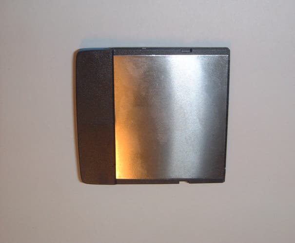
OXTLSE039R2
May 30, 2002Compact Flash Card Interface to Bluetooth
Equipment Class
DSS - Part 15 Spread Spectrum Transmitter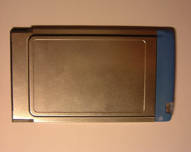
OXTLSE041R2
Apr 16, 2002Bluetooth PC card for Host
Equipment Class
DSS - Part 15 Spread Spectrum Transmitter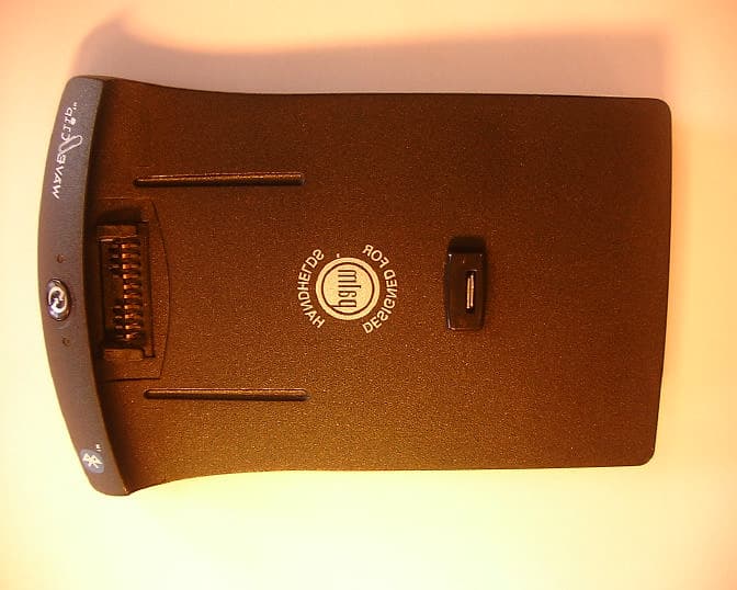
OXTLSE044
Nov 25, 2001Bluetooth Adapter for Palm V Handhelds
Equipment Class
DSS - Part 15 Spread Spectrum Transmitter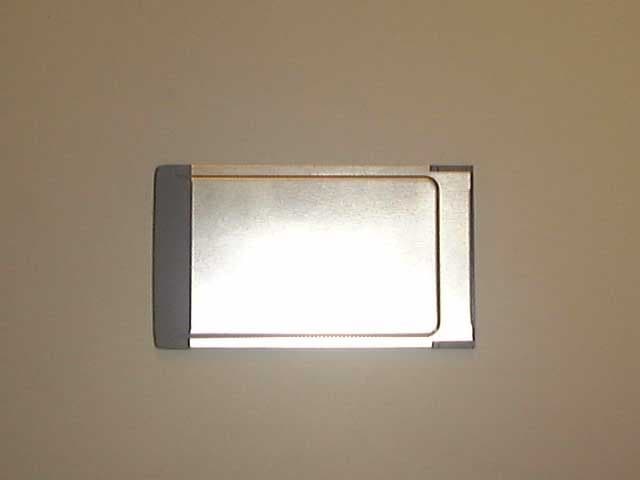
OXTLSE041
Mar 22, 2001PCMCIA card for host enabled Bluetooth devices
Equipment Class
DSS - Part 15 Spread Spectrum Transmitter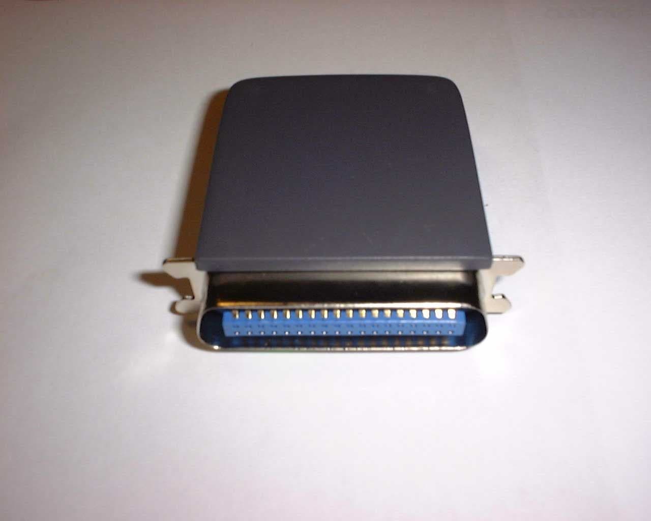
OXTLSE019
Mar 22, 2001Proprietary wireless printer module
Equipment Class
DSS - Part 15 Spread Spectrum Transmitter