PJU24002.4GHz 40 Channel Analog Modulation Cordless Phone
Shenzhen Jingneng Telecom Technology Co Ltd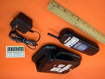
Click to zoom
Application Details
- Equipment Class
- DXX - Part 15 Low Power Communication Device Transmitter
- Date of Grant
- Mar 27, 2002
- Application Purpose
- Original Equipment
- Date of Application
- Mar 27, 2002
- Equipment Note
- 2.4GHz 40 Channel Analog Modulation Cordless Phone
- Frequency Range
- 2474.00000000 - 2475.95000000
- Country
- China
Documents & Files
Document Text
Text extracted from the exhibit documents filed with the FCC. Open a document above to read the original.
Block Diagram
GH2400L BASE BLOCK.sch-1 - Thu Feb 07 15:23:07 2002 OA FinePrint pdfFactory E°OAæ±¾½Ãà ̈ PDFhttp://www.fineprint.com GH2400L HAND BLOCK.sch-1 - Thu Feb 07 15:24:48 2002 OA FinePrint pdfFactory E°OAæ±¾½Ãà ̈ PDFhttp://www.fineprint.com
External Photos
External photos FCC ID: PJU2400 External photos FCC ID: PJU2400
Internal Photos
Internal photosFCC ID: PJU2400 Base assembly Base Main PCB comp s ide Internal photosFCC ID: PJU2400 Base Main PCB solder side Page key comp side Internal photosFCC ID: PJU2400 Page key solder side Base Oscillator PCB co mp side Internal photosFCC ID: PJU2400 Base Oscillator PCB so lde r side Internal photosFCC ID: PJU2400 Ha ndse t asse mbly Ha ndse t Main PCB co mp s ide Internal photosFCC ID: PJU2400 Handset Main PCB keypad side Ha ndse t Oscillato r PCB co mp s ide Internal photosFCC ID: PJU2400 Ha ndse t Oscillato r PCB solde r side
Operational Description
DESCRIPTION OF CIRCUIT OPERATION BASE UNIT : The demodulated signal, resulting from Double Super Heterodyne system, which appears at output Pin No.3 of CON1 is sent to U2 (COMPANDER IC) Pin No.16 for Expansion. The expended audio signal output from Pin No.19 is coupled to Q2,3 during the TALK mode. The audio signal is sent to the Telephone Line via hybrid Transformer HBY1. The demodulated data code from CON1 Pin No.3 is fed to Q5. It’s output is connected to Pin No.14(Data Reference Input Pin) and 15(Data input Pin) of IC3. The Audio signal receiving from TEL-LINE is inputted to U2 Pin No.8 for compression. The compressed audio signal from Pin No.1 of U2 is connected to Pin No.10 of CON1 for Audio signal modulation. Pin No.31 of IC3 generates data codes that should be transmitted to the hand set. the data code is connected to Pin No.10 of CON1 for Data modulation. Relay control is done by Pin No.18 of IC3. Ring signal monitored by U4 (PHOTO COUPLER IC) is detected by Pin No.16 of IC3 and Base Unit sends Ring Data Code to hand set. DTMF dialing is generated by IC3 Pin no.20~25 and this signal is sent to TEL-LINE through the Q2,Q3,Q4 and hybrid Transformer HYB1. When the hand set is placed on the base cradle, the charging is detected by Pin No.13 of IC3 and IC3 sends I.D data codes to handset for security code setting. When the handset is far away from base unit, squelch circuit of IC1 in RF part operates and Pin No.13 of IC1 goes “HI”. This Squelch Detection Signal will be detected by Pin No.17 of IC3 (the micro processor) and the base set goes to Stand-By mode after 20 sec. The power of the base set is supplied by U3(5V REGULATOR IC). LED display is controlled by Pin No.9 of IC3. HAND SET : The demodulated signal, resulting from Double Super Heterodyne system, which appears at output Pin No.3 of CON1 is connected to Pin No.16 of IC4(Expander input). The audio output from Pin No.19 of IC4(Expender output) is output to the Receiver unit with HAC compatibility through Q2. The demodulated data code from Pin No.3 of CON1 is fed to Q5. It’s output is connected to Pin No.14(Data Reference Input Pin) and 15(Data input Pin) of IC3. Voice signal from C-MIC is coupled to Pin No.8 of IC4. The voice signal is compressed by Compressor of IC4 and Voice signal output of Pin No.1(IC4) is connected to Pin no.10 of CON1 for Audio signal modulation. Pin No.23 of IC3 generates data codes that should be transmitted to the base set. the data code is connected to Pin No.10 of CON1 for Data modulation. During the charging, Charging is detected by Pin No.5 of IC3 Key board operation is monitored by Pin No.11,16~18,28~30 of IC3. Key Tone Signal and the ringing Signal from Pin No.9 of IC3 drives the BUZZER. 1. BASE RF MODULE 1) RX PART THE RECEIVER FRONT-END CONTAINS A BAND PASS FILTER, AND RF LOW NOISE AMPLIFIER, A ACTIVE TRANSISTOR MIXER, A CERAMIC FILTER AND 10.7MHz IF AMPLIFIER. ALSO IT INCLUDES BUFFER AMPLIFIERS FOR THE GENERATION OF LOCAL OSCILLATOR POWER. THIS FRONT-END RECEIVER RECEIVERS AND RF SIGNAL FROM THE ANTENNA. AND RF SIGNALS WITHIN THIS FREQUENCY RANGE IS 2474.MHz ~ 2475.95MHz PASS THROUGH RF AMP (Q1) AND BAND PASS FITER. AFTER PASSING THROUGH THE BAND PASS FILTER AND THE SIGNAL IS MIXED WITHIN 1’ST LOCAL FREQUENCY FROM VOLTAGE CONTROLLED OSCILLATOR. THE SIGNAL IS AMPLIFIED ON THE IF AMP TRANSISTOR (Q3) AND THE SIGNAL PASS THROUGH THE CERAMIC FILTER (10.7MHz). AFTER THE IF SIGNAL PASS THE CERAMIC FILTER, THE SIGNAL ENTER BY THE FM IF(INTERMEDIATE FREQUENCY) IC1. AND THE SIGNAL IS MIXED IN THE FM IF IC (DBL5018V). THE SIGNAL PASS THROUGH THE CERAMIC FILTER (450KHz). THE OUTPUT SIGNAL IN THE FM IF IC STREAMS FROM THE AF-OUT TERMINAL OF THE CONNECTOR TO THE BASE. FIG. 1 ANTENNA IC1 AF-OUT BPF F1 LNA Q1 VCO MIXER 1’ST LOCAL FREQUENCY F2 10.7MHz MC3361 IF IC DBL5018 GND 450KHz 2’nd LOCAL FREQ. TCXO 11.15MHz 2)TX PART THE SIGNAL IS MADE TO THE BASE, ENTER BY THE AF-IN TERMINAL OF THE CONNECTOR(CON1 OF PIN NO.10). THE SIGNAL SEND THE MOD TERMINAL OF THE TX VCO. THE SIGNAL IS MIXED IN THE TX VCO MIXING THE RF SIGNAL, THE RF SIGNAL ADJUST THE TRIMMER CAPACITOR (VC1). THE RF SIGNAL ENTER BY THE TRANSMISSION POWER AMP TRANSISTOR Q5 THE SINAL IS AMPLITUDE IN THE Q7. ENTER BY THE BAND PASS FILTER. THE RF SIGNAL PASS THROUGH THE BAND PASS FILTER, TO WARDS THE ANT. THE LAST TRANSMISSION RF SIGNAL IS 2402.55MHz ~ 2404.5MHz. FIG. 2 RF MODULE AF-IN VCO F4 2403MHz ANTENNA PLL IC IC2 Q5,7 ] TCXO 11.15MHz TREMMER CAP. VC1 2. PORTABLE RF MODULE 1) RX RART THE RECEIVER FRONT-END CONTAINS A BAND PASS FILTER,AND RF LOW NOISE AMPLIFIER, ACTIVE TRANSISTOR MIXER, CERAMIC FILTER AND 10.7MHz “IF” AMPLIFTER. ALSO IT INCLUDES BUFFER AMPLIFIERS OR THE GENERATION OF LOCAL OSCILLATOR POWER. THIS FRONT-END RECEIVERS AND RF SIGNAL FROM THE ANTENNA. AND RF SIGNALS WITHIN THIS FREQUENCY RANGE IS 2402.55MHz ~ 2404.5MHz PASS THROUGH RF AMP (Q1) AND BAND PASS FILTER.. AFTER PASSING THROUGH THE BAND PASS FILTER, THE SIGNAL IS MIXED WITHIN 1’ST LOCAL FREQUENCY FROM VOLTAGE CONTROLLED OSCILLATOR. THE SIGNAL IS AMPLIFIED ON THE IF AMP TRANSISTOR (Q3) AND THE SIGNAL PASS THROUGH THE CERANIC FILTER (10.7MHz) AFTER THE IF SIGNAL PASS THE MCF FILTER, THE SIGNAL ENTER BY THE FM IF (INTERMEDIATE FREQUENCY) IC. AND THE SIGNAL IS MIXED IN THE FM IF IC (DBL5018V). THE SIGNAL PASS THROUGH THE CERAMIC FILTER (450KHz). THE OUTPUT SIGNAL IN THE FM IF IC STREAMS FROM THE AF-OUT TERMINAL OF THE CONNECTOR 1 TO THE PORTABLE. FIG.3 ANTENNA IF IC DBL5018 F2 10. 7MHz 11. IC1 AF-OUT BPF F1 LNA Q1 VCO MIXER 1’ST LOCAL FREQUENCY 450KHz 2’nd LOCAL FREQ. TCXO 11.15MHz 2) TX PART THE SIGNAL IS MADE TO THE PORTABLE, ENTER BY THE AF-IN TERMINAL OF THE CONNECTOR. THE SIGNAL SEND THE MOD TERMINAL OF THE TX VCO. THE SIGNAL IS MIXED IN THE TX VCO MIXING THE RF SIGNAL, THE RF SIGNAL ADJUST THE TRIMMER CAPACITOR VC1. THE RF SIGNAL ENTER BY THE TRANSMISSION POWER AMP TRANSISTOR (Q5,7). ENTER BY THE BAND PASS FILTER. THE RF SIGNAL PASS THROUGH THE BAND PASS FILTER, TO WARDS THE …
Text truncated - open the document above for the full version.
Test Report
• The test results rep orted in this rep ort shall refer only to the samp le actually tested and shall not refer or be deemed to refer to bulk from which such a samp le may be said to have been obtained. • This rep ort shall not be rep roduced excep t in full without p rior authorization form Intertek Testing Services Limit ed FCC ID: PJU2400 Inte rte k Te sting Se rvice s Hong Kong Ltd. 2/F., Garment Centre, 576 Castle Peak Road, Kowloon, Hong Kong. Tel: (852) 2173 8888 Fax: (852) 2741 1693 Shenzhen Jingneng Telecom Technology Co., Ltd. Application For Certification 2.4GHz 40 Channel Analog Modulation Cordless Phone (FCC ID: PJU2400) WO# 0110208 TL/Ann Choy March 15, 2002 INTERTEK TESTING SERVICES FCC ID: PJU2400 i LIST OF EXHIBITS INTRODUCTION EXHIBIT 1 :General Description EXHIBIT 2 :System Test Configuration EXHIBIT 3 :Emission Results EXHIBIT 4 :Equipment Photographs EXHIBIT 5 :Product Labelling EXHIBIT 6 :Technical Specifications EXHIBIT 7 :Instruction Manual EXHIBIT 8 :Security Code Information INTERTEK TESTING SERVICES FCC ID: PJU2400 ii MEASUREMENT/TECHNICAL REPORT Shenzhen Jingneng Telecom Technology Co., Ltd. - MODEL: GH2400(XXX), CTP9400(XXX), CTP9402(XXX) FCC ID: PJU2400 This report concerns (check one:) Original Grant X Class II Change Equipment Type : Cordless Telephone (example : computer, modem, transmitter, etc.) Deferred grant requested per 47 CFR 0.457(d)(1)(ii)?Yes No X If yes, defer until : date Company Name agrees to notify the Commission by: date of the intended date of announcement of the product so that the grant can be issued on that date. Transition Rules Request per 15.37 ?Yes No X If no, assumed Part 15, Subpart C for intentional radiator - the new 47 CFR [ 12-18-01 Edition ] Provision. Report prepared by:Tommy Leung Intertek Testing Services. 2/F., Garment Centre, 576 Castle Peak Road, Kowloon, Hong Kong. Phone :852-2173-8538 Fax:852-2741-1693 INTERTEK TESTING SERVICES FCC ID: PJU2400 iii Table of Contents 1.0 General Description ....................................................................................................... 2 1.1 Product Description.................................................................................................... 2 1.2 Related Submittal(s) Grants........................................................................................ 3 1.3 Test Methodology....................................................................................................... 3 1.4 Test Facility................................................................................................................ 3 2.0 System Test Configuration ............................................................................................. 5 2.1 Justification................................................................................................................. 5 2.2 EUT Exercising Software ........................................................................................... 5 2.3 Support Equipment List and Description ................................................................... 6 2.4 Measurement Uncertainty .......................................................................................... 7 2.5 Equipment Modification............................................................................................. 7 3.0 Emission Results ............................................................................................................. 9 3.1 Field Strength Calculation ........................................................................................ 10 3.2 Radiated Emission Configuration Photograph - Base Unit ...................................... 11 3.3 Radiated Emission Data - Base Unit ........................................................................ 12 3.4 Radiated Emission Configuration Photograph - Handset ......................................... 15 3.5 Radiated Emission Data - Handset ........................................................................... 16 3.6 Radiated Emission on the bandedge......................................................................... 19 3.7 Line Conducted Configuration Photograph - Base Unit .......................................... 21 3.8 Line Conducted Emission Data - Base Unit ............................................................. 22 4.0 Equipment Photographs .............................................................................................. 25 5.0 Product Labelling ......................................................................................................... 27 6.0 Technical Specifications ............................................................................................... 29 7.0 Instruction Manual ....................................................................................................... 31 8.0 Security Code Information .......................................................................................... 33 INTERTEK TESTING SERVICES FCC ID: PJU2400 iv List of attached file Exhibit typeFile Descriptionfilename Test ReportTest Reportreport.doc Operation DescriptionTechnical Descriptiondescri.pdf Test Setup PhotoRadiated Emission for Baseconfig photos.doc Test Setup PhotoRadiated Emission for Handsetconfig photos.doc Test ReportEmission Plotemission.pdf Test Setup PhotoConducted Emissionconfig photos.doc Test ReportConducted Emission Test Resultconduct.pdf External PhotoExternal Photoexternal photos.doc Internal PhotoInternal Photointernal photos.doc Block DiagramBlock Diagramblock.pdf SchematicsCircuit Diagramcircuit.pdf ID Label/LocationLabel Artwork and Locationlabel.pdf User ManualUser Manualmanual.pdf User ManualFCC Informationfcc information.pdf INTERTEK TESTING SERVICES FCC ID: PJU2400 1 EXHIBIT 1 GENERAL DESCRIPTION INTERTEK TESTING SERVICES FCC ID: PJU2400 2 1.0 General Description 1.1 Product Description The GH2400(XXX) is a 2.4GHz 40 Channel Analog Modulation Cordless Phone. The unit…
Text truncated - open the document above for the full version.
Test Setup Photos
The Worst Case Configuration Photographs FCC ID: PJU2400 Radiated Emission – Base Front View Re ar Vie w The Worst Case Configuration Photographs FCC ID: PJU2400 Radiated Emission – Handset Front View Re ar Vie w The Worst Case Configuration Photographs FCC ID: PJU2400 Conducted Emission Front View Re ar Vie w The Worst Case Configuration Photographs FCC ID: PJU2400 Conducted Emission Side View
Contact Information
Applicant
Zheng Caian(QA Manager)
Technical Contact
Intertek Testing Services Hong Kong Ltd.Wilson Loke
[email protected]852-2173-8575
2/F., Garment Centre · Kowloon · Hong Kong
Non-Technical Contact
Intertek Testing Services Hong Kong Ltd.Wilson Loke
[email protected]852-2173-8575
Test Firm
Intertek Testing Services Hong KongBilly Chow
Technical Specifications
| # | Rule Parts | Frequency Range | Power Output |
|---|---|---|---|
| 2 | 15C | 2.47 GHz - 2.48 GHz | - |
Other Applications from Shenzhen Jingneng Telecom Technology Co Ltd
PJUGH9492
Jun 01, 20042.4G ANALOG CORDLESS PHONE WITH CID AND DAM
Equipment Class
DXX - Part 15 Low Power Communication Device Transmitter
PJU2400-01
Mar 18, 20032.4 GHz Cordless Telephone
Equipment Class
DXX - Part 15 Low Power Communication Device Transmitter
PJU2410-1
Feb 24, 2003Cordless Phone
Equipment Class
DXX - Part 15 Low Power Communication Device Transmitter
PJUHK250
Oct 24, 2002Cordless Telephone Base and Handset
Equipment Class
DXX - Part 15 Low Power Communication Device Transmitter
PJUGH3050
Jul 14, 20022.4GHz Cordless Phone
Equipment Class
DXT - Part 15 Low Power Transceiver, Rx Verified