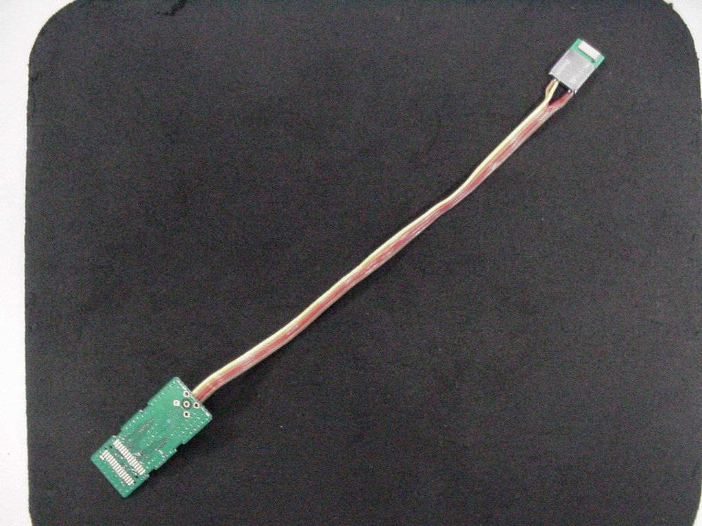
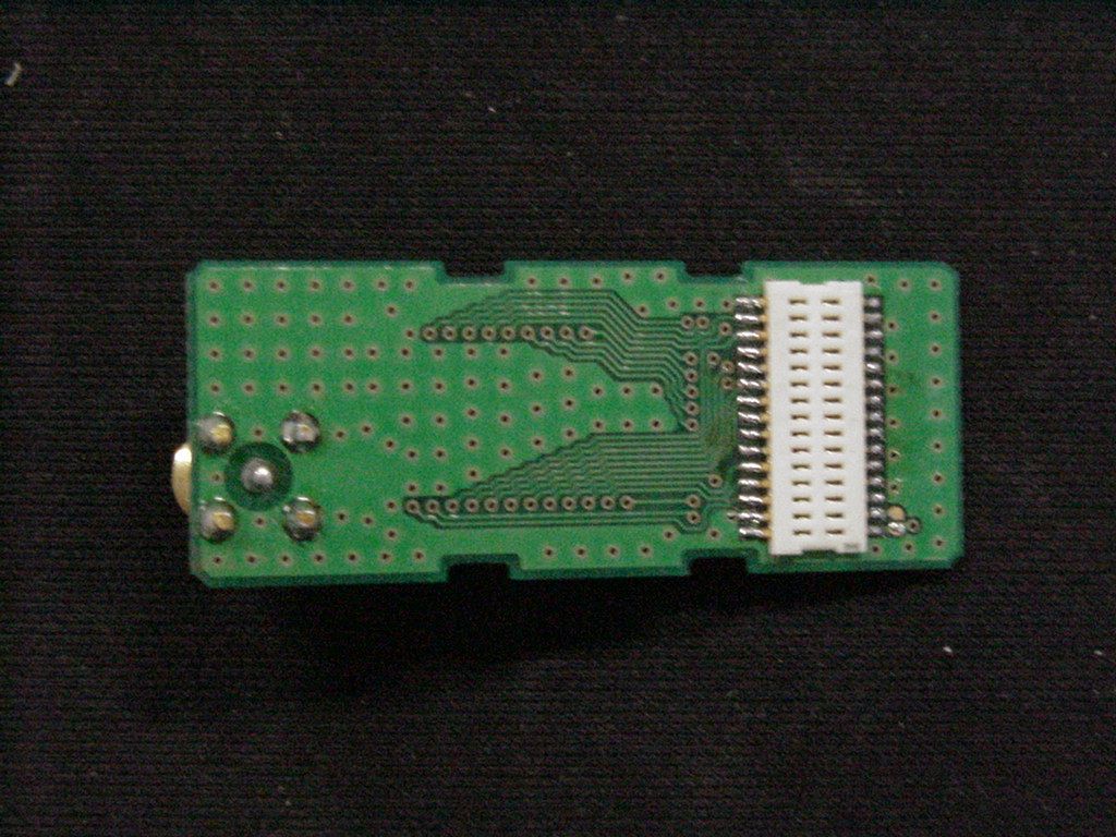
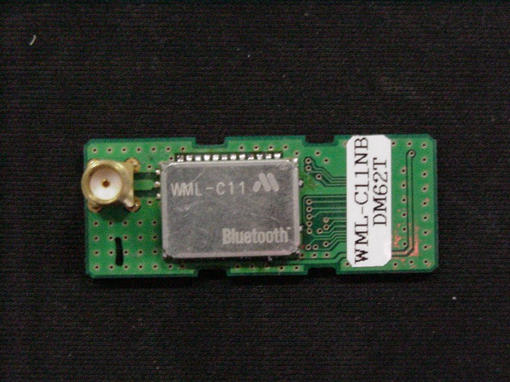
POOWML-C11XXBluetooth module
Mitsumi Electric Co., Ltd.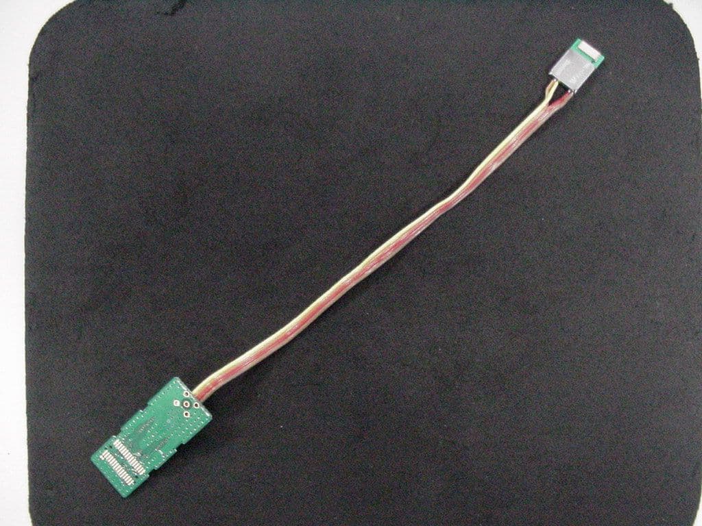
Click to zoom
Application Details
- Equipment Class
- DSS - Part 15 Spread Spectrum Transmitter
- Date of Grant
- Sep 26, 2002
- Application Purpose
- Original Equipment
- Date of Application
- Jul 30, 2002
- Equipment Note
- Bluetooth module
- Frequency Range
- 2402.00000000 - 2480.00000000
- Company
- Mitsumi Electric Co., Ltd.
- Country
- Japan
Documents & Files
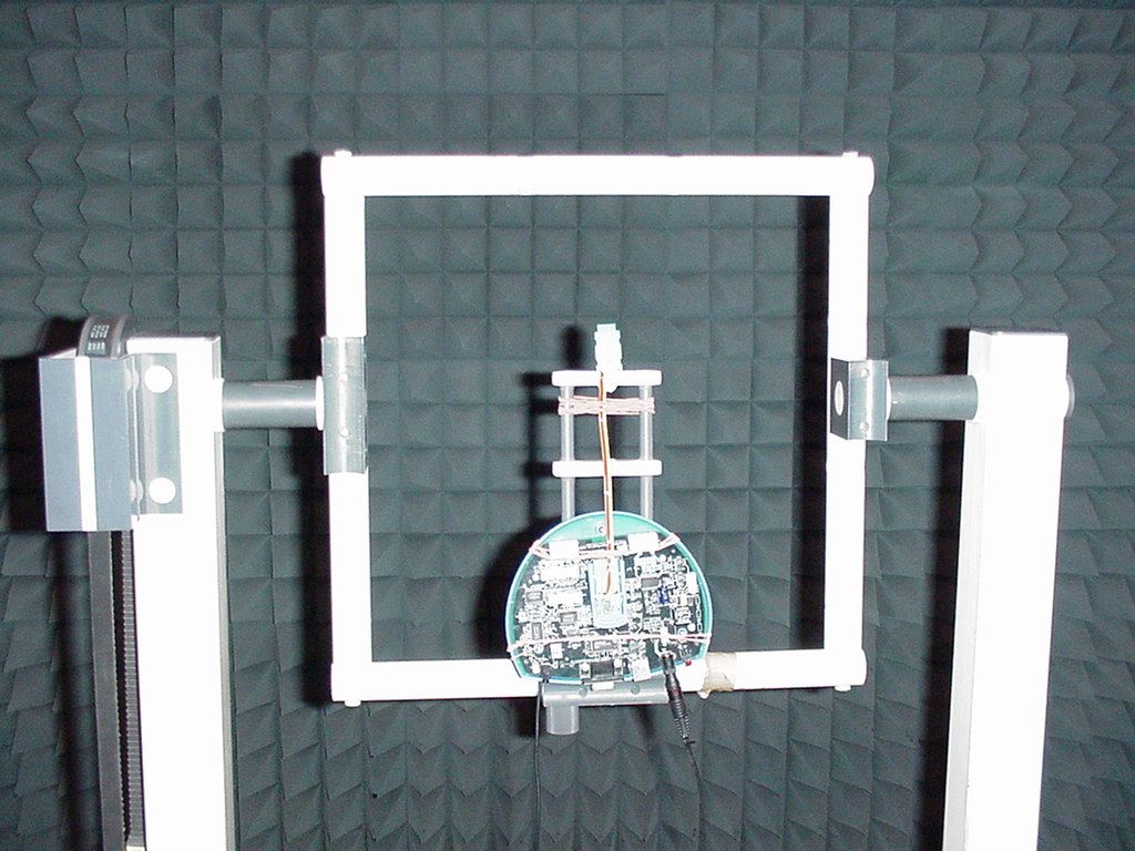
Document Text
Text extracted from the exhibit documents filed with the FCC. Open a document above to read the original.
Attestation Statements
Registergerichth registered in:Vorstandh Board of Directors:7 layers AG, Borsigstrasse 11 Ratingen HRB 3264Dr. Wolfgang Dahm40880 Ratingen, Germany AufsichtsratsvorsitzendehDr. Hans-Jürgen MeckelburgPhone: +49 (0) 2102 749 0 Chairman of the Supervisory Board:Fax: +49 (0) 2102 749 350 Dr. Sabine Grobeckerwww.7layers.com Annex Additional declaration part according FCC 15.247 for Bluetooth TM Devices Version: 2002-06-01 Annex - Additional declaration part according FCC 15.247 for Bluetooth devices Page 2 of 5 pages 1 Output power and channel separation of a Bluetooth device in the different operating modes: The different operating modes (data-mode, acquisition-mode) of a Bluetooth device don’t influence the output power and the channel spacing. There is only one transmitter which is driven by identical input parameters concerning these two parameters. Only a different hopping sequence will be used. For this reason the check of these RF parameters in one op-mode is sufficient. 2 Frequency range of a Bluetooth device: Hereby we declare that the maximum frequency of this device is: 2402 – 2480 MHz. This is according the Bluetooth Core Specification (+ critical errata) for devices which will be operated in the USA. This was checked during the Bluetooth Qualification tests (Test Case: TRM/CA/04-E). Other frequency ranges ( e.g. for Spain, France, Japan) which are allowed according the Core Specification are not supported by this device. 3 Co-ordination of the hopping sequence in data mode to avoid simultaneous occupancy by multiple transmitters: Bluetooth units which want to communicate with other units must be organised in a structure called piconet. This piconet consist of max. 8 Bluetooth units. One unit is the master the other seven are the slaves. The master co-ordinates frequency occupation in this piconet for all units. As the master hop sequence is derived from its BD address which is unique for each Bluetooth device, additional masters intending to establish new piconets will always use different hop sequences. 4 Example of a hopping sequence in data mode: Example of a 79 hopping sequence in data mode: 40, 21, 44, 23, 42, 53, 46, 55, 48, 33, 52, 35, 50, 65, 54, 67, 56, 37, 60, 39, 58, 69, 62, 71, 64, 25, 68, 27, 66, 57, 70, 59, 72, 29, 76, 31, 74, 61, 78, 63, 01, 41, 05, 43, 03, 73, 07, 75, 09, 45, 13, 47, 11, 77, 15, 00, 64, 49, 66, 53, 68, 02, 70, 06, 01, 51, 03, 55, 05, 04 Annex - Additional declaration part according FCC 15.247 for Bluetooth devices Page 3 of 5 pages 5 Equally average use of frequencies in data mode and behaviour for short transmissions: The generation of the hopping sequence in connection mode depends essentially on two input values: 1. LAP/UAP of the master of the connection 2. Internal master clock The LAP (lower address part) are the 24 LSB’s of the 48 BD_ADDRESS. The BD_ADDRESS is an unambiguous number of every Bluetooth unit. The UAP (upper address part) are the 24 MSB’s of the 48 BD_ADDRESS. The internal clock of a Bluetooth unit is derived from a free running clock which is never adjusted and is never turned off. For synchronisation with other units only offset are used. It has no relation to the time of the day. Its resolution is at least half the RX/TX slot length of 312.5 μs. The clock has a cycle of about one day (23h30). In most case it is implemented as 28 bit counter. For the deriving of the hopping sequence the entire LAP (24 bits), 4 LSB’s (4 bits) (Input 1) and the 27 MSB’s of the clock (Input 2) are used. With this input values different mathematical procedures (permutations, additions, XOR- operations) are performed to generate the sequence. This will be done at the beginning of every new transmission. Regarding short transmissions the Bluetooth system has the following behaviour: The first connection between the two devices is established, a hopping sequence was generated. For transmitting the wanted data the complete hopping sequence was not used. The connection ended. The second connection will be established. A new hopping sequence is generated. Due to the fact that the Bluetooth clock has a different value, because the period between the two transmission is longer (and it cannot be shorter) than the minimum resolution of the clock (312.5 μs). The hopping sequence will always differ from the first one. 6 Receiver input bandwidth and behaviour for repeated single or multiple packets: The input bandwidth of the receiver is 1 MHz. In every connection one Bluetooth device is the master and the other one is the slave. The master determines the hopping sequence (see chapter 5). The slave follows this sequence. Both devices shift between RX and TX time slot according to the clock of the master. Additionally the type of connection (e.g. single or multislot packet) is set up at the beginning of the connection. The master adapts its hopping frequency and its TX/RX timing according to the packet type of the connection. Also the slave of the connection will use these settings. Repeating of a packet has no influence on the hopping sequence. The hopping sequence generated by the master of the connection will be followed in any case. That means, a repeated packet will not be send on the same frequency, it is send on the next frequency of the hopping sequence. Annex - Additional declaration part according FCC 15.247 for Bluetooth devices Page 4 of 5 pages 7 Dwell time in data mode The dwell time of 0.3797s within a 30 second period in data mode is independent from the packet type (packet length). The calculation for a 30 second period is a follows: Dwell time = time slot length * hop rate / number of hopping channels *30s Example for a DH1 packet (with a maximum length of one time slot) Dwell time = 625 μs * 1600 1/s / 79 * 30s = 0.3797s (in a 30s period) For multislot packet the hopping is reduced according to the length of the packet. Example for a DH5 packet (with a maximum length of five time slots) Dwell time = 5 * 625 μs * 1600 * 1/5 *1/s / 79 * 30s = …
Text truncated - open the document above for the full version.
Attestation Statements
Registergerichth registered in:Vorstandh Board of Directors:7 layers AG, Borsigstrasse 11 Ratingen, HRB 3264Dr. Wolfgang Dahm40880 Ratingen, Germany AufsichtsratsvorsitzendehDr. Hans-Jürgen MeckelburgPhone: +49 (0) 2102 749 0 Chairman of the Supervisory Board:Fax: +49 (0) 2102 749 350 Dr. Sabine Grobeckerwww.7Layers.com Torsten Lohoff 31. July 2002 Phone +49 (0) 2102 749 306 Fax +49 (0) 2102 749 350 request for a modular approval - FCC ID: POOWML-C11XX Dear Application Examiner, In some of the documents related to the Mitsumi modular approval application, slightly different type numbers are used. The FCC ID identifying the equipment is POOWML-C11XX. In some documents, the type numbers followed by ## or XX can be found. The '##' or 'XX' characters are used as substitute symbols for the identification of production series without any hardware differences. There will be some space between the type number and the substitutes on the identification label to make it clear that the substitutes are not a part of the type number. Independent from this type numbers, the FCC-ID is POOWML-C11XX. Please contact us if you have any additional questions. Best Regards 7layers AG FCC Federal Communications Commission 4_MITSU_0102_BTT
Cover Letter(s)
Registergerichth registered in:Vorstandh Board of Directors:7 layers AG, Borsigstrasse 11 Ratingen, HRB 3264Dr. Wolfgang Dahm40880 Ratingen, Germany AufsichtsratsvorsitzendehDr. Hans-Jürgen MeckelburgPhone: +49 (0) 2102 749 0 Chairman of the Supervisory Board:Fax: +49 (0) 2102 749 350 Dr. Sabine Grobeckerwww.7Layers.com Torsten Lohoff 31. July 2002 Phone +49 (0) 2102 749 306 Fax +49 (0) 2102 749 350 application for equipment certification, FCC-ID: POOWML-C11XX Dear Application Examiner, we hereby submit the application for certification for the WML-C11 Bluetooth module on behalf of Mitsumi Electronics Co. Ltd. This application is a modular approval application for a device operating in the frequency range of 2.4 to 2.4835 GHz. The maximum measured peak power output is 17,2 dBm (52,48 mW). The document 'Exhibits' gives an overview about the submitted documents Best Regards Torsten Lohoff 7layers AG FCC Federal Communications Commission 4_MITSU_0102_BTT
Cover Letter(s)
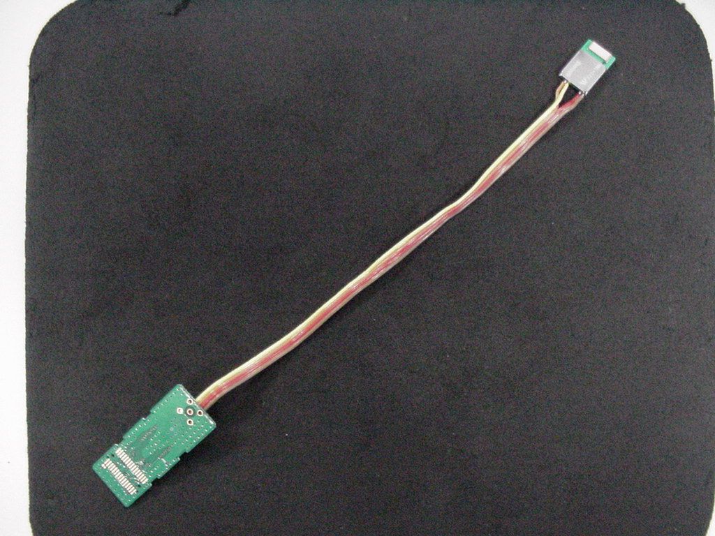
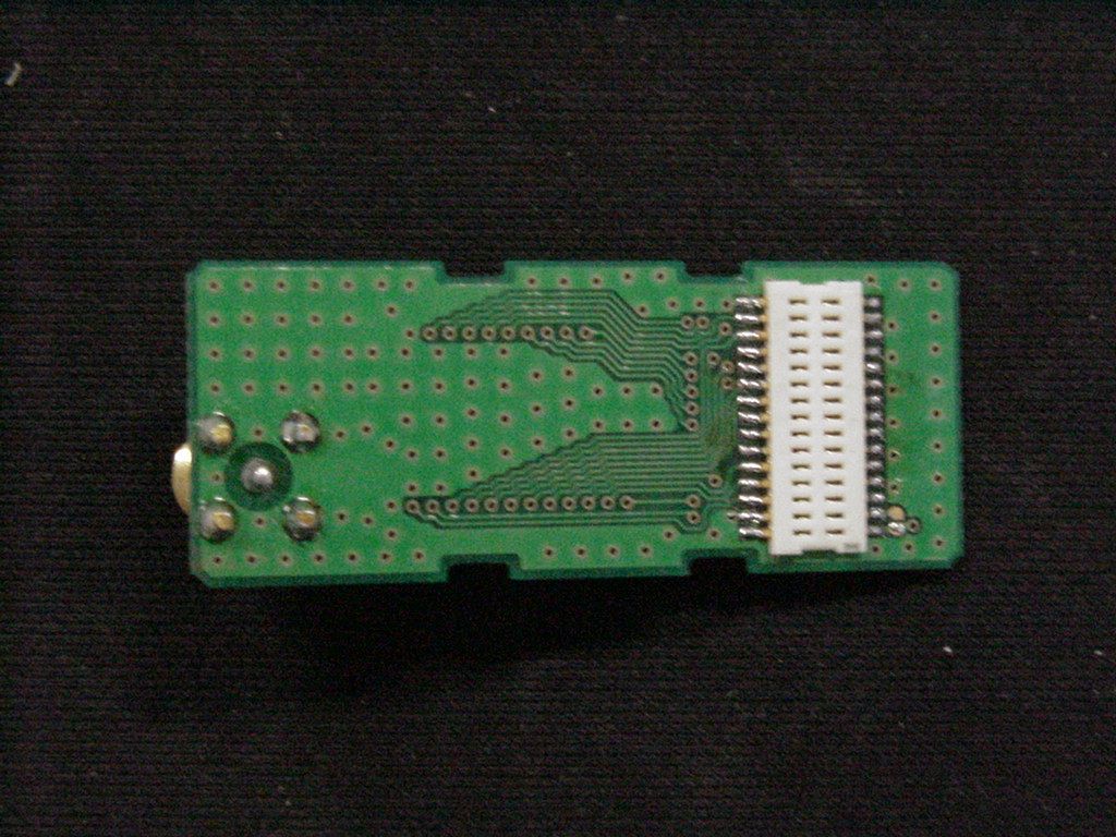
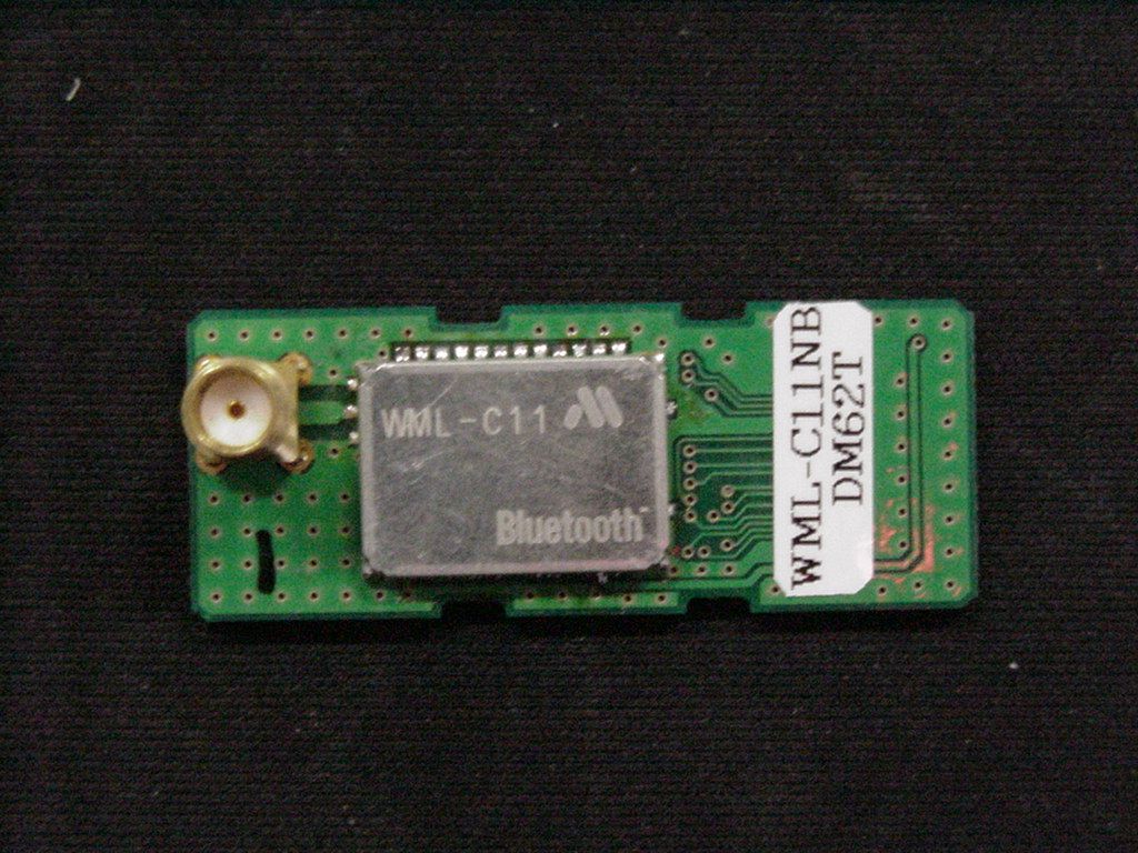
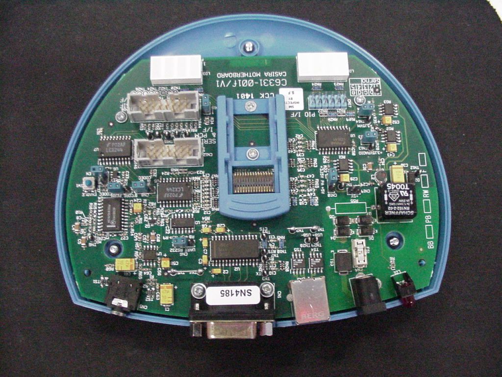
Exhibits for the modular approval application Mitsumi WML-C11 (FCC-ID: POOWML-C11XX) Exhibit description file name confi- dential A Agent authorization letter Commercial Power of Attorney WML-C09###, WML-C10###, WML-C11###.pdf no B FCC Part 15.247 test report 4_mitsu_0102_BTT_FCCb.pdf no C technical description functional_description_WML-C11##_r1.0.pdf no D FCC ID label Logo-WML-C11###_r2.0.pdf no E Schematics Circuit_Diagram_WML-C11##_r1.0.pdf yes F PCB layouts Printed_circuit_board_layout_WML- C11##_r1.0.pdf yes G Parts List Parts_List_WML-C11##_r1.0.pdf yes H1 WML_C11rad_top.jpg no H2 WML-C11_bottom.jpg no H3 Photos: PCB top and bottom WML-C11_top.jpg no J Request for confidentiality FCC_confidential_WML-C11##_r2.0.pdf no K Block diagram Blockdiagram_WML-C11##_r1.0.pdf yes L Bluetooth hopping description and add. info additional_declaration_FCC_15_247.pdf no M Declaration about antenna configurations Declaration_about_antenna_configurations_WM L-C11##_r1.0.pdf no O1 CASIRA_01_open_top.jpg no O2 Photos: test setup test_setup-C11.jpg no P FCC fee payment letter fee_payment_letter.jpg no Q FCC fee payment form 159 form159-WML-C11.jpg no R modular approval requirements request_modular_approval_WML-C11.pdf no S reference design application Reference_Design_Application_WML- C11##_r1.0.pdf yes U users guide functional_description_WML-C11##_r1.0.pdf no V declaration FCC-ID and used type numbers declaration_type_numbers_WML-C11.pdf no W Labelling instructions for the end product manufacturer Instruction_Manual_for_FCCID_WML- C11##_r2.0 no
Cover Letter(s)
Page 1 of 1 Request for confidentiality 31th Jul 2002 COMMERCIAL IN CONFIDENCE This material may not in whole or part be copied, stored electronically or communicated to third parties without MITSUMI ELECTRIC CO., LTD’s prior agreement in writing. Request for confidentiality about MITSUMI ELECTRIC CO., LTD IUT name: Bluetooth Module WML-C11## grantee code: POOWML-C grantee code: POOWML-Cgrantee code: POOWML-C grantee code: POOWML-C11XX 11XX11XX 11XX According to the exhibit list provided to the FCC, we hereby request the confidentiality for the following exhibits: E: Schematics F: PCB layouts G: Parts list K: Block diagram S: Reference design application The relevant fee has been paid with the application. Thank you very much.
Cover Letter(s)
Registergerichth registered in:Vorstandh Board of Directors:7 layers AG, Borsigstrasse 11 Ratingen, HRB 3264Dr. Wolfgang Dahm40880 Ratingen, Germany AufsichtsratsvorsitzendehDr. Hans-Jürgen MeckelburgPhone: +49 (0) 2102 749 0 Chairman of the Supervisory Board:Fax: +49 (0) 2102 749 350 Dr. Sabine Grobeckerwww.7Layers.com Torsten Lohoff 09. July 2002 Phone +49 (0) 2102 749 306 Fax +49 (0) 2102 749 350 request for a modular approval - FCC ID: POOWML-C11XX Dear Application Examiner, the Mitsumi Bluetooth module WML-C11 is seeking FCC authorization as a modular transmitter. The requirement of the FCC Public notice DA00-1407 are met. The following requirements are fulfilled: 1. The modular transmitter must have its own RF shielding The radio portion of the module is contained in its own RF shielding. See photos in exhibit H. 2. The modular transmitter must have buffered modulation/data inputs The module has a memory management unit inside of the IC. It buffers the data inputs from UART and USB terminal. 3. The modular transmitter must have its own power supply regulation The IC contains an own voltage regulation. In case of changes in the supply voltage VCC (for example caused by temperature changes or other effects), the internal voltage will be stabilized. FCC Federal Communications Commission 4_MITSU_0102_BTT - 2 - 4. The modular transmitter must comply with the antenna requirements of Section 15.203 and 15.204c The transmitter shall only be used with the tested integral antenna or with an antenna that has less antenna gain. Requirements for the use of external antennas are specified in Exhibit M 5. The modular transmitter must be tested in a stand-alone configuration The EUT was tested in a stand-alone configuration. The module was fixed in the Casira Development Kit of CSR (Cambridge Silicon Radio) during the test. See also test report (Exhibit B) and Test setup photos (Exhibit O). For radiated measurements, the required distance of 10 cm was ensured by a special connector. 6. The modular transmitter must be labelled with its own FCC ID number The EUT will be labelled with its own FCC ID number. The label is specified in Exhibit D. If the module is installed inside of an end-product, the label will not be visible. In this case the OEM customer will be instructed to how to apply the exterior label. 7. The modular transmitter must comply with any specific rule or operating requirements applicable to the transmitter and the manufacturer must provide adequate instructions along with the module to explain any such requirements. The EUT is compliant with all applicable FCC rules. Detail instructions are given in the Users Guide (see Exhibit U) 8. The modular transmitter must comply with any applicable RF exposure requirements. The maximum measured power output is 52,48 mW (17,20 dBm), the maximum antenna gain is 2,14 dBi = numeric gain 1,637 (see also FCC test report - Exhibit B) The maximum permissable exposure is defined in 47 CFR 1.1310 with 1 mW/cm². The distance from the EUT's transmitting antenna where the exposure level reaches the maximum permitted level is calculated using the general equation: S = P*G / 4πR² S max = 1mW/cm², P = 52,48 mW, linear power gain relative to the isotropic radiator = 2,14 dBi = 1,637 (numeric gain), R = distance in cm Solving for R, the 1mW/cm² limit is reached in a distance of 2,61 cm to the transmitting antenna. The module has to be integrated in a way that the minimum distance of 2,61 cm is ensured so a statement in the users manual is not necessary. In case that the distance of 2,61 cm cannot be ensured, the users manual of the end product in which the module will be integrated has to inform the user about a minimum distance of 20 cm between the equipment and the body if the equipment is considered as mobile equipment. If the equipment is considered as portable equipment, an evaluation against the applicable SAR limits is required. Please contact us if you have any additional questions. Best Regards 7layers AG
Cover Letter(s)
Registergerichth registered in:Vorstandh Board of Directors:7 layers AG, Borsigstrasse 11 Ratingen, HRB 3264Dr. Wolfgang Dahm40880 Ratingen, Germany AufsichtsratsvorsitzendehDr. Hans-Jürgen MeckelburgPhone: +49 (0) 2102 749 0 Chairman of the Supervisory Board:Fax: +49 (0) 2102 749 350 Dr. Sabine Grobeckerwww.7Layers.com Torsten Lohoff 31.07.2002 Phone +49 (0) 2102 749 306 Fax +49 (0) 2102 749 350 fee payments Dear Sirs, please find enclosed two remittance advice forms 159 for the payment of the equipment authorization fees for our customer Mitsumi Electronics Co., Ltd. Both forms have been filled according to the instructions in the FCC fee filing guide. They contain payments for the certification fee and the request for confidentiality for two applications. If you have any questions, do not hesitate to contact me. Best Regards Federal Communications Commission c/o Mellon Bank Center Att. Wholesale Lockbox Shift Supervisor Three Mellon Bank Center 525 William Penn Way 27 th Floor, Room 153-2713 Pittsburgh, PA 15259-0001 USA Projektname: 4_MITSU_0102_BTT
ID Label/Location Info
Page 1 of 1 Instruction manual for FCC ID labeling 31th Jul 2002 COMMERCIAL IN CONFIDENCE This material may not in whole or part be copied, stored electronically or communicated to third parties without MITSUMI ELECTRIC CO., LTD’s prior agreement in writing Instruction manual for FCC ID labeling IUT name:Bluetooth Module WML-C11## FCC-ID:POOWML-C11XX This is intend to infrom you how to specify the FCC ID of our Bluetooth module WML-C11## on your end product. Based on the Public Notice from FCC, you should have a label on the pruduct which indicates that it contains our Bluetooth module. And the lavel should use wording such as "Contains FCC ID: POOWML-C11XX." It shows an example below Any similar wording that expresses the same meaning may be used. Contains FCC ID: POOWML-C11XX
Operational Description
Functional Description 21/May/2002 MITSUMI Bluetooth Module “ WML-C11##” Hardware:Version 1 Ultra-small and thin size achieved through use of high density mounting technology . 1. APPLICATIONS Notebook PCs, mobile phones, digital cameras, PC peripherals, PDA. 2. DESCRIPTIONS Wireless communication module conforming to Bluetooth Ver.1.1. 3. FEATURES 1 ) Ultra-small and thin size achieved through use of high density mounting technology. 2 ) High sensitivity. 3 ) UART, USB and PCMIF interfaces enable wide range of applications. 4 ) Conforms to FCC, CE and other countries’ EMI standards. 5 ) Supports Bluetooth Class1. Note)The BLUETOOTH trademarks are owned by Bluetooth SIG,INC.,U.S.A. 4. SPECIFICATIONS I t e m S p e c i f i c a t i o n s F r e q u e n c y 2402 to 2480MHz M o d u l a t i o n FHSS / GFSK Channel intervals 1 M H z Number of channels 7 9 C H Power supply voltage 3.3V(typ.) ,3.2 to 3.4V Transmission rate 7 2 1 k b p s Receive sensitivity -80dBm typ. Output level (Class1) 20dBm max. TM ©1998-2000 MITSUMI Electronics Corp. All rights reserved.MITSUMI is a trademark of MITSUMI Electronics Corporation. Other company names and products names are trademarks of their respective companies. Product specifications are subject to revisions or changes without notification. 5. TERMINAL DESCRIPTION No.SymbolI/ODescription 1GNDGround 2SPI_MOSIISynchronous Serial Interface data input (N.C.*) 3PIO [6]I/OProgrammable I/O line 4PIO [7]I/OProgrammable I/O line 5RESETIReset if high 6SPI_CLKISynchronous Serial Interface Clock (N.C.*) 7PCM_CLKI/OSynchronous PCM data clock 8PCM_SYNCI/OSynchronous data strobe 9PCM_INISynchronous PCM data input 10PCM_OUTOSynchronous PCM data out 11VDDOperating supply voltage is 3.3V+/-0.1V 12GNDGround 13UART_RXIAsynchronous Serial Data Input 14UART_TXOAsynchronous Serial Data Output 15UART_RTSOAsynchronous Serial Data RTS 16UART_CTSIAsynchronous Serial Data CTS 17USB D+USB D+ line 18USB D-USB D- line 19PIO [2] / USB PULL UPI/OProgrammable I/O line. / USB Pull-Up 20PIO [3] / USB RESUMEI/OProgrammable I/O line. / Output goes high to wake up PC when USB mode 21PIO [5]I/OProgrammable I/O line. 22PIO [4]I/OProgrammable I/O line. 23SPI_CSBIChip select for Synchronous Serial Interface (N.C.*) 24SPI_MISOOSynchronous Serial Interface data output (N.C.*) 25GNDGround 26ANTI/ORF input/output 27GNDGround 28GNDGround 29GNDGround * N.C.=OPEN **5V tolerant input terminal. 6. BLOCK DIAGRAM 7. PCM IF PCM_OUT, PCM_IN, PCM_CLK, PCM_SYNC carry one of bi-directional channel of voice data using 13bits PCM at 8ks/s. PCM_SYNC operates at a fixed clock frequency of 8kHz. PCM_CLK operates at a fixed clock frequency of 256kHz. Bits 1 to 13 of the PCM_OUT data carry the current output sample value. Bits 14 to 16 carry a three bit signal level value. Reference PCM audio device is MC145483. RF Receiver RF Transmitter 2nd Synthesizer Baseband Controller Memor y Management RAM XT Driver VDD BC2-UART / BC2-USB 1st Synthesizer 16bits Micro- Processor PIO SPI CSB SPI CLK SPI _MOSI SPI MISO SPI PCM/IF MEMORY DRIVER UART TX UART UART_RX UART _RTS UART CTS PCM OUT PCM _IN PCM _SYNC PCM CLK External- Flash ROM 256k x 16 bits PIO[2...7] BL ANT BPF 16MHz cr ystal REG RF SW PA USB D+ USB USB D- 8. OVERALL APPEARANCE Module without antenna WML-C11N# Module with antenna WML-C11A#
RF Exposure Info
Registergerichth registered in:Vorstandh Board of Directors:7 layers AG, Borsigstrasse 11 Ratingen, HRB 3264Dr. Wolfgang Dahm40880 Ratingen, Germany AufsichtsratsvorsitzendehDr. Hans-Jürgen MeckelburgPhone: +49 (0) 2102 749 0 Chairman of the Supervisory Board:Fax: +49 (0) 2102 749 350 Dr. Sabine Grobeckerwww.7Layers.com Torsten Lohoff 09. July 2002 Phone +49 (0) 2102 749 306 Fax +49 (0) 2102 749 350 request for a modular approval - FCC ID: POOWML-C11XX Dear Application Examiner, the Mitsumi Bluetooth module WML-C11 is seeking FCC authorization as a modular transmitter. The requirement of the FCC Public notice DA00-1407 are met. The following requirements are fulfilled: 1. The modular transmitter must have its own RF shielding The radio portion of the module is contained in its own RF shielding. See photos in exhibit H. 2. The modular transmitter must have buffered modulation/data inputs The module has a memory management unit inside of the IC. It buffers the data inputs from UART and USB terminal. 3. The modular transmitter must have its own power supply regulation The IC contains an own voltage regulation. In case of changes in the supply voltage VCC (for example caused by temperature changes or other effects), the internal voltage will be stabilized. FCC Federal Communications Commission 4_MITSU_0102_BTT - 2 - 4. The modular transmitter must comply with the antenna requirements of Section 15.203 and 15.204c The transmitter shall only be used with the tested integral antenna or with an antenna that has less antenna gain. Requirements for the use of external antennas are specified in Exhibit M 5. The modular transmitter must be tested in a stand-alone configuration The EUT was tested in a stand-alone configuration. The module was fixed in the Casira Development Kit of CSR (Cambridge Silicon Radio) during the test. See also test report (Exhibit B) and Test setup photos (Exhibit O). For radiated measurements, the required distance of 10 cm was ensured by a special connector. 6. The modular transmitter must be labelled with its own FCC ID number The EUT will be labelled with its own FCC ID number. The label is specified in Exhibit D. If the module is installed inside of an end-product, the label will not be visible. In this case the OEM customer will be instructed to how to apply the exterior label. 7. The modular transmitter must comply with any specific rule or operating requirements applicable to the transmitter and the manufacturer must provide adequate instructions along with the module to explain any such requirements. The EUT is compliant with all applicable FCC rules. Detail instructions are given in the Users Guide (see Exhibit U) 8. The modular transmitter must comply with any applicable RF exposure requirements. The maximum measured power output is 52,48 mW (17,20 dBm), the maximum antenna gain is 2,14 dBi = numeric gain 1,637 (see also FCC test report - Exhibit B) The maximum permissable exposure is defined in 47 CFR 1.1310 with 1 mW/cm². The distance from the EUT's transmitting antenna where the exposure level reaches the maximum permitted level is calculated using the general equation: S = P*G / 4πR² S max = 1mW/cm², P = 52,48 mW, linear power gain relative to the isotropic radiator = 2,14 dBi = 1,637 (numeric gain), R = distance in cm Solving for R, the 1mW/cm² limit is reached in a distance of 2,61 cm to the transmitting antenna. The module has to be integrated in a way that the minimum distance of 2,61 cm is ensured so a statement in the users manual is not necessary. In case that the distance of 2,61 cm cannot be ensured, the users manual of the end product in which the module will be integrated has to inform the user about a minimum distance of 20 cm between the equipment and the body if the equipment is considered as mobile equipment. If the equipment is considered as portable equipment, an evaluation against the applicable SAR limits is required. Please contact us if you have any additional questions. Best Regards 7layers AG
Test Report
EMC Measurement/Technical Report 4_MITSU_0102_BTT_FCCb on 7 Layers AG Borsigstr. 11 40880 Ratingen Germany Note: The following test results relate only to the devices specified in this document. This report shall not be reproduced in parts without the written approval of the testing laboratory. Bluetooth™ Module WML-C11 Registergericht - registered in: Ratingen, HRB 3264 Aufsichtratsvorsitzende - Chairman of the Supervisory Board: Dr. Sabine Grobecker Vorstand - Board of Directors: Dr. Wolfgang Dahm Dr. Hans-Jürgen Meckelburg 7 layers AG, Borsigstrasse 11 40880 Ratingen, Germany Phone: +49 (0) 2102 749 0 Fax: +49 (0) 2102 749 350 http://www.7Layers.com Report Reference: Table of Contents 0. Summary 0.1 Technical Report Summary 0.2 Measurement Summary 1. Administrative Data 1.1 Testing Laboratory 1.2 Project Data 1.3 Applicant Data 1.4 Manufacturer Data 3. Testobject Data 3.1 General EUT Description 3.2 EUT Main Components 3.3 Ancillary Equipment 3.4 EUT Setups 3.5 Operating Modes 4. Measurement Results Conducted Emissions Occupied Bandwidth Output Power Spurious Emissions Conducted 5. Testequipment 6. Foto Report 7. Setup Drawings 3 3 4 6 6 6 6 6 8 8 9 9 9 10 11 - 11 14 17 28 30 33 35 Spurious Emissions Radiated19 2. Product Labeling 2.1 FCC ID Label 2.2 Location of Label on the EUT 7 7 7 Dwell Time Power Density Channel Separation Processing Gain 23 25 27 - - 4.1 4.2 4.3 4.4 4.5 4.6 4.7 - 8. Annex Measurement plots25 Pages Page 2 of 59Testreport Reference: 4_MITSU_0102_BTT_FCCb 0 Summary 0.1 Technical Report Summary Type of Authorization: Certification for an Intentional Radiator (Frequency Hopping Spread Spectrum) Applicable FCC Rules: Prepared in accordance with the requirements of FCC Rules and Regulations as listed in 47 CFR Ch.1 Parts 0 to 19 (10-1-98 Edition). The following subparts are applicable to the results in this test report. Part 2, Subpart J - Equipment Authorization Procedures, Certification Sections Part 15, Subpart C - Intentional Radiators § 15.201 Equipment authorization requirement § 15.203 Antenna requirements § 15.207 Conducted limits § 15.209 Radiated emission limits; general requirements § 15.247 Operation within the bands 902-928 MHz, 2400-2483,5 MHZ and 5725-5850 MHz Summary Test Results: The equipment under test fulfilled the requirements of the applied FCC rules. Note: The tests were selected and performed with reference to the FCC Public Notice DA 00- 705, released March 30, 2000 Page 3 of 59Testreport Reference: 4_MITSU_0102_BTT_FCCb 0.2 Measurement Summary § 15.247 (a) (1) (ii)FCC Part 15, Subpart C ANSI C63.41992The measurement was performed according to Occupied BandwidthOccupied Bandwidth OP-ModeOP-ModeSetupSetupPortPortFinal ResultFinal Result setup 1op-mode 1temporary antenna connectorpassed setup 1op-mode 2temporary antenna connectorpassed setup 1op-mode 3temporary antenna connectorpassed setup 1op-mode 4temporary antenna connectorpassed setup 1op-mode 5temporary antenna connectorpassed § 15.247 (b) (1)FCC Part 15, Subpart C FCC §15.3110-1-1998The measurement was performed according to Peak Power OutputPeak Power Output OP-ModeOP-ModeSetupSetupPortPortFinal ResultFinal Result setup 1op-mode 1temporary antenna connectorpassed setup 1op-mode 2temporary antenna connectorpassed setup 1op-mode 3temporary antenna connectorpassed setup 1op-mode 4temporary antenna connectorpassed setup 1op-mode 5temporary antenna connectorpassed § 15.247 (c)FCC Part 15, Subpart C FCC §15.3110-1-1998The measurement was performed according to Spurious RF Conducted EmissionsSpurious RF Conducted Emissions OP-ModeOP-ModeSetupSetupPortPortFinal ResultFinal Result setup 1op-mode 1temporary antenna connectorpassed setup 1op-mode 2temporary antenna connectorpassed setup 1op-mode 3temporary antenna connectorpassed § 15.247 (c), §15.35 (b), § 15.209FCC Part 15, Subpart C ANSI C63.41992The measurement was performed according to Spurious Radiated EmissionsSpurious Radiated Emissions OP-ModeOP-ModeSetupSetupPortPortFinal ResultFinal Result setup 2op-mode 1enclosurepassed setup 2op-mode 2enclosurepassed setup 2op-mode 3enclosurepassed § 15.247 (g)FCC Part 15, Subpart C FCC §15.3110-1-1998The measurement was performed according to Dwell TimeDwell Time OP-ModeOP-ModeSetupSetupPortPortFinal ResultFinal Result setup 1op-mode 4temporary antenna connectorpassed setup 1op-mode 5temporary antenna connectorpassed § 15.247 (g)FCC Part 15, Subpart C Page 4 of 59Testreport Reference: 4_MITSU_0102_BTT_FCCb FCC §15.3110-1-1998The measurement was performed according to Power DensityPower Density OP-ModeOP-ModeSetupSetupPortPortFinal ResultFinal Result setup 1op-mode 4temporary antenna connectorpassed setup 1op-mode 5temporary antenna connectorpassed § 15.247 (a) (1)FCC Part 15, Subpart C FCC §15.3110-1-1998The measurement was performed according to Channel SeparationChannel Separation OP-ModeOP-ModeSetupSetupPortPortFinal ResultFinal Result setup 1op-mode 6temporary antenna connectorpassed Responsible for Accreditation Scope: Responsible for Test Report: Page 5 of 59Testreport Reference: 4_MITSU_0102_BTT_FCCb 1. Administrative Data 1.1 Testing Laboratory Company Name: Address: The test facility is also accredited by the following accreditation organisation: Responsible for Accreditation Scope: 7 Layers AG Borsigstr. 11 40880 Ratingen Germany DAR-Registration no. TTI-P-G 178/99-10 Dipl.-Ing Bernhard Retka Dipl.-Ing Arndt Stöcker This facility has been fully described in a report submitted to the FCC and accepted in a letter dated February 07, 2000 under the registration number 96716. - Deutscher Akkreditierungs Rat 17.05.02 Dipl.-Ing. Robert Machulec 27.06.02 20.05-22.05.02; 16.06.02 Responsible for Test Report: Receipt of EUT: Date of Test(s): Date of Report: 1.2 Project Data Mitsumi Electronics Co. Ltd. Mr. Takashi Watanabe 8-8-2, Kokuryo-cho chohu-shi, 182-8557 Tokyo Japan ZIP 182-8557 see applicant 1.4 Manufacturer Data Company Name: Address: Contact Person: Company Name: Address: Contact Person: 1.…
Text truncated - open the document above for the full version.
Contact Information
Applicant
Katsunori Kobari(Mr.)
Technical Contact
Mitsumi Electric Co. Ltd.Ryoji Waki
[email protected]+81 283 23 3332
8-8-2, Kokuryo-cho · Tokyo · Japan
Non-Technical Contact
7layers AGTorsten Lohoff
[email protected]+49 2102 749 306
Test Firm
7layers AGRobert Machulec
Technical Specifications
| # | Rule Parts | Frequency Range | Power Output |
|---|---|---|---|
| 1 | 15C | 2.40 GHz - 2.48 GHz | 52.48 mW |
Other Applications from Mitsumi Electric Co., Ltd.
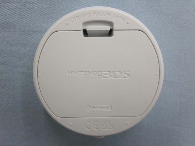
POOCTR012
Feb 07, 2015RFID Product
Equipment Class
DXX - Part 15 Low Power Communication Device Transmitter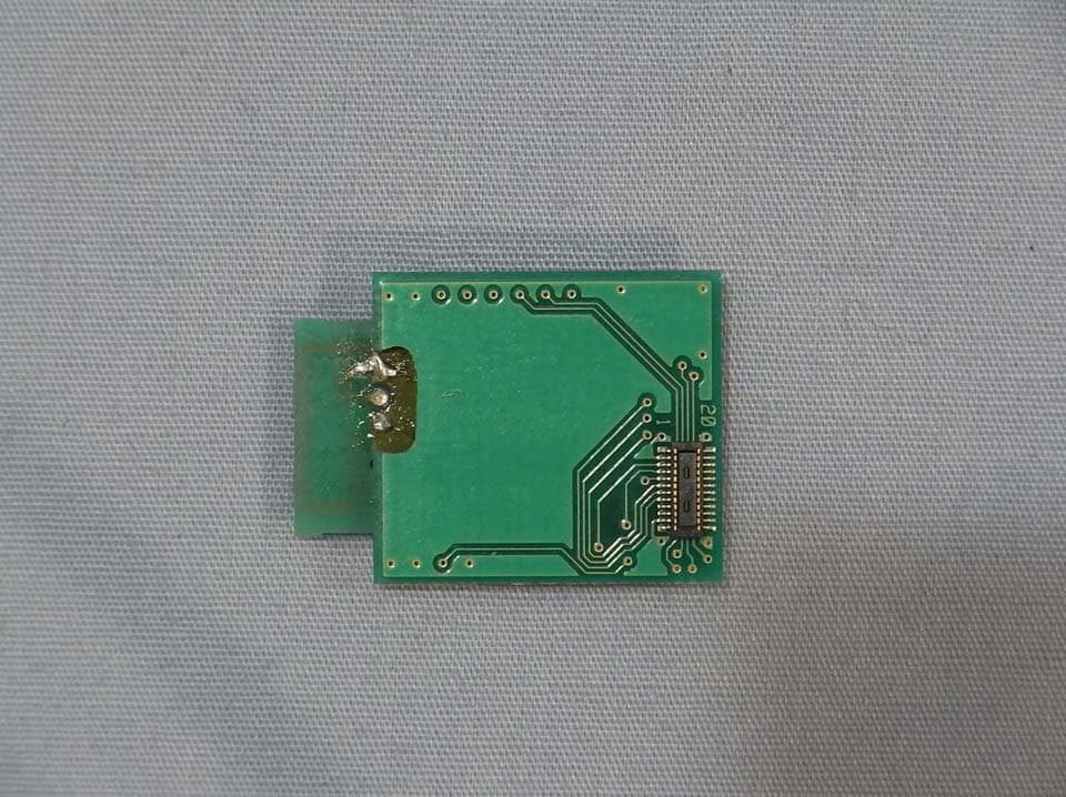
POO-WC75
Jan 07, 2014Bluetooth LE Module
Equipment Class
DTS - Digital Transmission System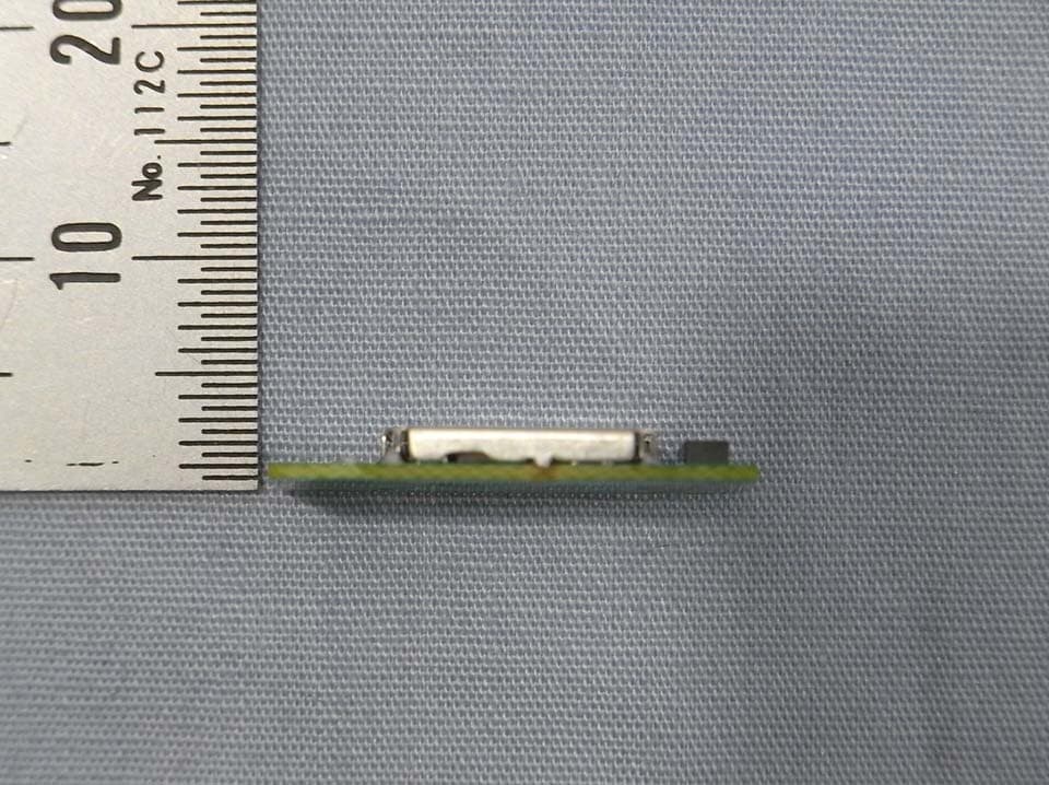
POO-WC69
Apr 24, 2013Bluetooth LE Module
Equipment Class
DTS - Digital Transmission System
POO-R237999
Jul 10, 2012Remote Controller
Equipment Class
DSS - Part 15 Spread Spectrum TransmitterPOO-DR237973
Mar 24, 2012Remote Controller
Equipment Class
DSS - Part 15 Spread Spectrum Transmitter