PPQWN4320IEEE 802.11g Mbps Wireless LAN USB Adapter
LITE-ON TECHNOLOGY CORP.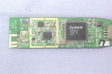
Click to zoom
Application Details
- Equipment Class
- DTS - Digital Transmission System
- Date of Grant
- Jun 27, 2004
- Application Purpose
- Original Equipment
- Date of Application
- Jun 27, 2004
- Equipment Note
- IEEE 802.11g Mbps Wireless LAN USB Adapter
- Frequency Range
- 2412.00000000 - 2462.00000000
- Company
- LITE-ON TECHNOLOGY CORP.
- Country
- Taiwan
Documents & Files
Document Text
Text extracted from the exhibit documents filed with the FCC. Open a document above to read the original.
Users Manual
FCC Statement FCC ID : PPQ-WN4320 This device complies with Part15 FCC Rules. Operation is Subject to the following two conditions : (1)This device may not cause harmful interference. (2)This device must accept any interference received including interference that may cause undesired operation
Users Manual
FCC Statement FCC ID : PPQ-WN4320 This device complies with Part15 FCC Rules. Operation is Subject to the following two conditions : (1)This device may not cause harmful interference. (2)This device must accept any interference received including interference that may cause undesired operation
Users Manual
CAUTION FCC RF Radioation Exposure Statement : This equipment complies with FCC RF radiation exposure limits set forth for an uncontrolled environment. This device and its antenna must not be co-located or operating in conjection with any other antenna or transmitter. Evaluation for compliance with FCC RF exposures has only been perform when installed and used in a typical laptop computer. Use of this transmitting card in other devices such as tablets and PDAs is not authorized. FCC Statement FCC ID : PPQ-WN4320 This device complies with Part15 FCC Rules. Operation is Subject to the following two conditions : (1)This device may not cause harmful interference. (2)This device must accept any interference received including interference that may cause undesired operation
Block Diagram
WN4320Z Functional Block Diagram USB 2.0 /1.1 Host LED*2 OSC 40MHZ POWER 3.3/2.8/1.8V SE2525L ZD1211 EEROM 32K RF2959 AS179-92 RF Front End Ethernet Front End
Block Diagram
WN4320Z Functional Block Diagram USB 2.0 /1.1 Host LED*2 OSC 40MHZ POWER 3.3/2.8/1.8V SE2525L ZD1211 EEROM 32K RF2959 AS179-92 RF Front End Ethernet Front End
External Photos
Compliance Certification Services Inc. Report No: 40526001 Date of Issue: June 4, 2004 Page 1 of 10 EXTERNAL PHOTOGRPHS OF EUT Compliance Certification Services Inc. Report No: 40526001 Date of Issue: June 4, 2004 Page 2 INTERNAL PHOTOGRPHS OF EUT Compliance Certification Services Inc. Report No: 40526001 Date of Issue: June 4, 2004 Page 3
External Photos
Compliance Certification Services Inc. Report No: 40526001 Date of Issue: June 4, 2004 Page 1 of 10 EXTERNAL PHOTOGRPHS OF EUT Compliance Certification Services Inc. Report No: 40526001 Date of Issue: June 4, 2004 Page 2 INTERNAL PHOTOGRPHS OF EUT Compliance Certification Services Inc. Report No: 40526001 Date of Issue: June 4, 2004 Page 3
Internal Photos
Compliance Certification Services Inc. Report No: 40526001 Date of Issue: June 4, 2004 Page 1 of 10 EXTERNAL PHOTOGRPHS OF EUT Compliance Certification Services Inc. Report No: 40526001 Date of Issue: June 4, 2004 Page 2 INTERNAL PHOTOGRPHS OF EUT Compliance Certification Services Inc. Report No: 40526001 Date of Issue: June 4, 2004 Page 3
Internal Photos
Compliance Certification Services Inc. Report No: 40526001 Date of Issue: June 4, 2004 Page 1 of 10 EXTERNAL PHOTOGRPHS OF EUT Compliance Certification Services Inc. Report No: 40526001 Date of Issue: June 4, 2004 Page 2 INTERNAL PHOTOGRPHS OF EUT Compliance Certification Services Inc. Report No: 40526001 Date of Issue: June 4, 2004 Page 3
Operational Description
ZyDAS WLAN Solution ZD1211_DS_006_PDF-1.doc ZD11-001 ZyDAS Confidential 2 2004/3/15 Function Diagram Function Description Reset ZD1211 provides build-in power on reset circuit generates stable reset signal for the whole chip that was derived from external supply power in power on time. The voltage threshold detection and ripple counter circuit are designed to eliminate un-stable state in power on stage. Power Control The ZD1211 considers the power state in WLAN application and USB specification requirement. The different power states are defined as followings: Normal Operation state: While WLAN operates, all chip function is active. MAC controller is in operating all the time. To save the current consumption in this state, transmission function of baseband processor is gated during receiving, and the receiving function is gated during transmission. Power Saving State: When ZD1211 operates in 802.11 power saving mode, the chip will gated the clock to Microcontroller, MAC and baseband processor. The 40Mhz OSC still working to keep USB alive. In the state, only a timer circuit in the chip still operates. After the timer timeout, the chip is wakeup for protocol handling. USB suspend State: When the host system slept or enter hibernate mode, ZD1211will enter USB suspend mode. ZD1211 asserts the pin PDN40M to shutdown 40Mhz OSC. In this power state, all the circuit in ZD1211 is in the clock gated state and only static current is consumed. After receive resume signal from USB host, the pin PDN40M will be de-alert automatically. Then the 40Mhz OSC starts beating and enter normal operation mode. Power mode Power State Clock 40M Micro controller MACBasebandUSB State State Enter Condition State Leave Condition Normal operation On 40M 40M 40M Connect NA NA Power saving On Gated Gated Gated Connect Power saving ATIM timer timeout USB suspend Shutdown Gated Gated Gated Suspend USB Suspend USB Resume MAC Controller FIFO Baseband Processor USB 2.0 Micro Controller EEPROM Controlle r UART RF Interface Power management LED ICE PLL Serial EEPROM UART LEDs RFDigital RF Analog USB 2.0 Clock 40Mhz 12Mhz Power on Reset Digital VDD Digital Ground Mode selection Analog VDD Analog Ground PDN40M External Memory Control GPIO GPIOs/ Memory Control ZyDAS WLAN Solution ZD1211_DS_006_PDF-1.doc ZD11-001 ZyDAS Confidential 3 2004/3/15 Clock ZD1211 MAC and baseband operates in 40Mhz clock. The pin 40MCLKI connects to 40Mhz OSC which provides the clock. The USB clock pin XSCI may come from external 12M OSC or use the pin 12MCLKO that derived from internal PLL. Mode Selection There are configurable pins may be set as external memory control signals or GPIO pins. Mode selection pins mode 0 and mode 1 decide the options. The mode selection pins are detected on power on stage. Mode1/Mode0 Low/Low Low/High Pin Number External Memory GPIO 85,86,87,88,89,90,91,92MD[7:0] Reserved 97 MA0 SGPIO0 98 MA1 SGPIO1 99 MA2 SGPIO2 100 MA3 SGPIO3 101 MA4 SGPIO4 102 MA5 SGPIO5 103 MA6 Reserved 104 MA7 Reserved 79 MA8 Reserved 80 MA9 Reserved 83 MA10 Reserved 81 MA11 Reserved 105 MA12 Reserved 78 MA13 Reserved 106 MA14 Reserved 82 MOE_N Reserved 84 MCE_N Reserved 77 MWE_N Reserved USB 2.0 Interface USB 2.0 interface is fully compatible to 480M USB high speed mode and 12M full speed mode. It integrates USB 2.0 physical layer transceiver and controller in chip. The embedded microcontroller and serial EEPROM provide flexibility for customization of card identification in USB enumeration. ICE These pins are used for debug purpose only. Serial EEPROM Interface ZD1211 needs a 32K bit serial EEPROM to provide the card identification on booting stage and RF information on operation. The interface also provides software interface to read and write EEPROM. UART The UART may operate in 115200, 57600, 38400, 19200, 9600 baud rate. The interface can be provided for debug purpose or for specific feature. LED Two LED pins are provided for indication of WLAN operation. The behavior of LED may be programmable by software on host system. ZyDAS WLAN Solution ZD1211_DS_006_PDF-1.doc ZD11-001 ZyDAS Confidential 4 2004/3/15 GPIO There are 6 general purpose IO pins provided for specific application. All these pins are configurable and software programmable to input or output. In input mode, it may generate interrupt to micro controller for event handling. These pin are default in input state when power on reset. These pins are pin MUX with external memory control pins. The mode selection pins decide the option. More GPIO pins may be derived from RF interface pins. If used RFMD RF2959 then some pins may used as general purpose output. RF GPIO pins Pin Name 34 B6 42 B1 35 B5 41 B2 29 SHDNB External Memory Control The external memory control pins may connect to 8 bit SRAM or Flash memory. The memory access range may up to 32K byte. These pins are pin MUX with GPIO pins. The mode selection pins decide the option. If more external memory is required, it may use RF GPIO to connect more address lines. RF Interface There are kinds of RF interface allowed to connect to ZD1211. ZD1211 provides programmable interface flexibility to hook lots of RF transceivers. RXIQ interface The common mode voltage for the RXIQ is 1.6V typically (Maximum 1.7, Minimum 1.4). If the RXIQ common mode voltage from RF transceiver is greater than 1.4V and less than 1.7V, then DC couple is recommended. Otherwise, AC couple will be used. When AC couple is used, 0.1uF is recommended. The I,Q ADC input resistance (single) is 25 kΩ typically (maximum 28kΩ, minimum 21kΩ). The I,Q ADC input capacitance (single) is 3.3 pF typically (maximum 2.54pF, minimum 3.06 pF). RX AGC interface ZD1211 supports 2 RX AGC interface: digital RX AGC (B1-B7) and analog RX AGC (RX_VGC). For Maxim MAX2825, B1-B7 and RXHP are used to support digital RX AGC. B7 and B6 control the LNA gain([B7,B6]=[1,1] high gain; [B7,B6]=[1,0] middle gain; [B7,B6]=[0,x] low gain); B5-B1 control baseband VGA gain; RXHP controls HPF (High Pass Fil…
Text truncated - open the document above for the full version.
Operational Description
ZyDAS WLAN Solution ZD1211_DS_006_PDF-1.doc ZD11-001 ZyDAS Confidential 2 2004/3/15 Function Diagram Function Description Reset ZD1211 provides build-in power on reset circuit generates stable reset signal for the whole chip that was derived from external supply power in power on time. The voltage threshold detection and ripple counter circuit are designed to eliminate un-stable state in power on stage. Power Control The ZD1211 considers the power state in WLAN application and USB specification requirement. The different power states are defined as followings: Normal Operation state: While WLAN operates, all chip function is active. MAC controller is in operating all the time. To save the current consumption in this state, transmission function of baseband processor is gated during receiving, and the receiving function is gated during transmission. Power Saving State: When ZD1211 operates in 802.11 power saving mode, the chip will gated the clock to Microcontroller, MAC and baseband processor. The 40Mhz OSC still working to keep USB alive. In the state, only a timer circuit in the chip still operates. After the timer timeout, the chip is wakeup for protocol handling. USB suspend State: When the host system slept or enter hibernate mode, ZD1211will enter USB suspend mode. ZD1211 asserts the pin PDN40M to shutdown 40Mhz OSC. In this power state, all the circuit in ZD1211 is in the clock gated state and only static current is consumed. After receive resume signal from USB host, the pin PDN40M will be de-alert automatically. Then the 40Mhz OSC starts beating and enter normal operation mode. Power mode Power State Clock 40M Micro controller MACBasebandUSB State State Enter Condition State Leave Condition Normal operation On 40M 40M 40M Connect NA NA Power saving On Gated Gated Gated Connect Power saving ATIM timer timeout USB suspend Shutdown Gated Gated Gated Suspend USB Suspend USB Resume MAC Controller FIFO Baseband Processor USB 2.0 Micro Controller EEPROM Controlle r UART RF Interface Power management LED ICE PLL Serial EEPROM UART LEDs RFDigital RF Analog USB 2.0 Clock 40Mhz 12Mhz Power on Reset Digital VDD Digital Ground Mode selection Analog VDD Analog Ground PDN40M External Memory Control GPIO GPIOs/ Memory Control ZyDAS WLAN Solution ZD1211_DS_006_PDF-1.doc ZD11-001 ZyDAS Confidential 3 2004/3/15 Clock ZD1211 MAC and baseband operates in 40Mhz clock. The pin 40MCLKI connects to 40Mhz OSC which provides the clock. The USB clock pin XSCI may come from external 12M OSC or use the pin 12MCLKO that derived from internal PLL. Mode Selection There are configurable pins may be set as external memory control signals or GPIO pins. Mode selection pins mode 0 and mode 1 decide the options. The mode selection pins are detected on power on stage. Mode1/Mode0 Low/Low Low/High Pin Number External Memory GPIO 85,86,87,88,89,90,91,92MD[7:0] Reserved 97 MA0 SGPIO0 98 MA1 SGPIO1 99 MA2 SGPIO2 100 MA3 SGPIO3 101 MA4 SGPIO4 102 MA5 SGPIO5 103 MA6 Reserved 104 MA7 Reserved 79 MA8 Reserved 80 MA9 Reserved 83 MA10 Reserved 81 MA11 Reserved 105 MA12 Reserved 78 MA13 Reserved 106 MA14 Reserved 82 MOE_N Reserved 84 MCE_N Reserved 77 MWE_N Reserved USB 2.0 Interface USB 2.0 interface is fully compatible to 480M USB high speed mode and 12M full speed mode. It integrates USB 2.0 physical layer transceiver and controller in chip. The embedded microcontroller and serial EEPROM provide flexibility for customization of card identification in USB enumeration. ICE These pins are used for debug purpose only. Serial EEPROM Interface ZD1211 needs a 32K bit serial EEPROM to provide the card identification on booting stage and RF information on operation. The interface also provides software interface to read and write EEPROM. UART The UART may operate in 115200, 57600, 38400, 19200, 9600 baud rate. The interface can be provided for debug purpose or for specific feature. LED Two LED pins are provided for indication of WLAN operation. The behavior of LED may be programmable by software on host system. ZyDAS WLAN Solution ZD1211_DS_006_PDF-1.doc ZD11-001 ZyDAS Confidential 4 2004/3/15 GPIO There are 6 general purpose IO pins provided for specific application. All these pins are configurable and software programmable to input or output. In input mode, it may generate interrupt to micro controller for event handling. These pin are default in input state when power on reset. These pins are pin MUX with external memory control pins. The mode selection pins decide the option. More GPIO pins may be derived from RF interface pins. If used RFMD RF2959 then some pins may used as general purpose output. RF GPIO pins Pin Name 34 B6 42 B1 35 B5 41 B2 29 SHDNB External Memory Control The external memory control pins may connect to 8 bit SRAM or Flash memory. The memory access range may up to 32K byte. These pins are pin MUX with GPIO pins. The mode selection pins decide the option. If more external memory is required, it may use RF GPIO to connect more address lines. RF Interface There are kinds of RF interface allowed to connect to ZD1211. ZD1211 provides programmable interface flexibility to hook lots of RF transceivers. RXIQ interface The common mode voltage for the RXIQ is 1.6V typically (Maximum 1.7, Minimum 1.4). If the RXIQ common mode voltage from RF transceiver is greater than 1.4V and less than 1.7V, then DC couple is recommended. Otherwise, AC couple will be used. When AC couple is used, 0.1uF is recommended. The I,Q ADC input resistance (single) is 25 kΩ typically (maximum 28kΩ, minimum 21kΩ). The I,Q ADC input capacitance (single) is 3.3 pF typically (maximum 2.54pF, minimum 3.06 pF). RX AGC interface ZD1211 supports 2 RX AGC interface: digital RX AGC (B1-B7) and analog RX AGC (RX_VGC). For Maxim MAX2825, B1-B7 and RXHP are used to support digital RX AGC. B7 and B6 control the LNA gain([B7,B6]=[1,1] high gain; [B7,B6]=[1,0] middle gain; [B7,B6]=[0,x] low gain); B5-B1 control baseband VGA gain; RXHP controls HPF (High Pass Fil…
Text truncated - open the document above for the full version.
RF Exposure Info
©2004 SPORTON International Inc..SAR Testing Lab This report shall not be reproduced except in full, without the written approval of Sporton. Rev.02 FCC SAR Test Report Test Report No ﹕ O451402-1-2-02 Specific Absorption Rate (SAR) Test Report for LITE-ON TECHNOLOGY CORP. on the IEEE 802.11g, 54Mbps Wireless LAN USB Adapter Report No. : O451402-1-2-02 Trade Name : LITE-ON, Pro-Nets, SpeedCom+, NetoDragon Model Name : WN4320Z/ US54GZ FCC ID : PPQ-WN4320 Date of Testing : June 01、26, 2004 Date of Report.: June 26, 2004 Date of Review : June 26, 2004 The test results refer exclusively to the presented test model / sample only. Without written approval of SPORTON International Inc., the test report shall not be reproduced except in full. SPORTON International Inc. 6F, No.106, Sec. 1, Hsin Tai Wu Rd., Hsi Chih, Taipei Hsien, Taiwan, R.O.C. ©2004 SPORTON International Inc..SAR Testing Lab Tel:886-22696-2468 Fax:886-2-2696-2255 FCC SAR Test Report Test Report No ﹕ O451402-1-2-02 Table of Contents 1. Statement of Compliance ............................................................................................................................................................ 1 2. Administration Data ................................................................................................................................................................... 2 2.1. Testing Laboratory ............................................................................................................................................................. 2 2.2. Detail of Applicant.............................................................................................................................................................. 2 2.3. Detail of Manfacturer ......................................................................................................................................................... 2 2.4. Application Detail .............................................................................................................................................................. 2 3. Scope............................................................................................................................................................................................. 3 3.1. Description of Device Under Test (DUT) ........................................................................................................................... 3 3.2. Product Photo..................................................................................................................................................................... 4 3.3. Applied Standards: ............................................................................................................................................................. 5 3.4. Device Category and SAR Limits ....................................................................................................................................... 6 3.5. Test Conditons .................................................................................................................................................................... 6 3.5.1. Ambient Condition: ..................................................................................................................................................... 6 3.5.2. Test Configuration: ...................................................................................................................................................... 6 4. Specific Absorption Rate (SAR) ................................................................................................................................................. 7 4.1. Introduction ........................................................................................................................................................................ 7 4.2. SAR Definition .................................................................................................................................................................... 7 5. SAR Measurement Setup............................................................................................................................................................ 8 5.1. DASY4 E-Field Probe System............................................................................................................................................. 9 5.1.1. ET3DV6 E-Field Probe Specification ....................................................................................................................... 10 5.1.2. ET3DV6 E-Field Probe Calibration .......................................................................................................................... 10 5.2. DATA Acquisition Electronics (DAE) ................................................................................................................................11 5.3. Robot ................................................................................................................................................................................ 12 5.4. Measurement Server ......................................................................................................................................................... 12 5.5. SAM Twin Phantom .......................................................................................................................................................... 12 5.6. Data Storage and Evaluation ........................................................................................................................................... 14 5.6.1. Data Storage .............................................................................................................................................................. 14 5.6.2. Data Evaluation .....................................................................…
Text truncated - open the document above for the full version.
RF Exposure Info
©2004 SPORTON International Inc..SAR Testing Lab This report shall not be reproduced except in full, without the written approval of Sporton. Rev.02 FCC SAR Test Report Test Report No ﹕ O451402-1-2-02 Specific Absorption Rate (SAR) Test Report for LITE-ON TECHNOLOGY CORP. on the IEEE 802.11g, 54Mbps Wireless LAN USB Adapter Report No. : O451402-1-2-02 Trade Name : LITE-ON, Pro-Nets, SpeedCom+, NetoDragon Model Name : WN4320Z/ US54GZ FCC ID : PPQ-WN4320 Date of Testing : June 01、26, 2004 Date of Report.: June 26, 2004 Date of Review : June 26, 2004 The test results refer exclusively to the presented test model / sample only. Without written approval of SPORTON International Inc., the test report shall not be reproduced except in full. SPORTON International Inc. 6F, No.106, Sec. 1, Hsin Tai Wu Rd., Hsi Chih, Taipei Hsien, Taiwan, R.O.C. ©2004 SPORTON International Inc..SAR Testing Lab Tel:886-22696-2468 Fax:886-2-2696-2255 FCC SAR Test Report Test Report No ﹕ O451402-1-2-02 Table of Contents 1. Statement of Compliance ............................................................................................................................................................ 1 2. Administration Data ................................................................................................................................................................... 2 2.1. Testing Laboratory ............................................................................................................................................................. 2 2.2. Detail of Applicant.............................................................................................................................................................. 2 2.3. Detail of Manfacturer ......................................................................................................................................................... 2 2.4. Application Detail .............................................................................................................................................................. 2 3. Scope............................................................................................................................................................................................. 3 3.1. Description of Device Under Test (DUT) ........................................................................................................................... 3 3.2. Product Photo..................................................................................................................................................................... 4 3.3. Applied Standards: ............................................................................................................................................................. 5 3.4. Device Category and SAR Limits ....................................................................................................................................... 6 3.5. Test Conditons .................................................................................................................................................................... 6 3.5.1. Ambient Condition: ..................................................................................................................................................... 6 3.5.2. Test Configuration: ...................................................................................................................................................... 6 4. Specific Absorption Rate (SAR) ................................................................................................................................................. 7 4.1. Introduction ........................................................................................................................................................................ 7 4.2. SAR Definition .................................................................................................................................................................... 7 5. SAR Measurement Setup............................................................................................................................................................ 8 5.1. DASY4 E-Field Probe System............................................................................................................................................. 9 5.1.1. ET3DV6 E-Field Probe Specification ....................................................................................................................... 10 5.1.2. ET3DV6 E-Field Probe Calibration .......................................................................................................................... 10 5.2. DATA Acquisition Electronics (DAE) ................................................................................................................................11 5.3. Robot ................................................................................................................................................................................ 12 5.4. Measurement Server ......................................................................................................................................................... 12 5.5. SAM Twin Phantom .......................................................................................................................................................... 12 5.6. Data Storage and Evaluation ........................................................................................................................................... 14 5.6.1. Data Storage .............................................................................................................................................................. 14 5.6.2. Data Evaluation .....................................................................…
Text truncated - open the document above for the full version.
Schematics
AA BB CC DD EE 4 4 3 3 2 2 1 1 (For USB) (For Analog) OSCILLATOR CIRCUIT FOR MAC/ RF USB2.0 5. D+,D- DISTANCE : 14 milNOTE : REFERENCE USB2.0 PCB LAYOUT GUIDELINES2. PP : 7 mil 90 ohm 3. WIDTH : 12 mil6. GROUND SEPARATION >=12 mil1. PCB : FR4 material (Er ~ 4.5)4. THICKNESS : 1/2 oz copper (0.7mil)7. BOARD THICKNESS ~ 62 mil (1.57 mm) For PCB Layout Only Default short LITEON Technology C orporation ZD1211 Circuit 01 ZD1211 Dongle USB WLAN Use RFMD RF2959 + SE2525L C 11 Tuesday, May 11, 2004 TitleSize Document Number Rev Date: Sheet of RF_VDD +3.3VA CLKINRFPDNMCLKMCLK +3.3V GND +1.8V USB_D-USB_D+ RXI_PRXI_NRXQ_NRXQ_P TXI-SEN GNDSCLK RXI_PTXQ+GNDAUSB_VBUS USB+5V 12MCLKOADC3-VREF-FSYNDATA PDNMCLK +3.3V+1.8V RXQ_P USB_DPRS +3.3VGNDGNDGNDLINK LNAGSTR_SW_EXTRAUSB_DMRS+3.3VAUSB_DP GND+3.3V SHUT_DOWN GND SYNCLK +3.3V+3.3V RX_VGC +1.8V GNDGNDGNDGND+1.8V +A3.3V TX_VGCGNDA MCLK GND RGNDADC3-VREF-HB2 +A3.3V +3.3VRGNDVBGCAPTXI+ GND VCM +3.3VARGNDRXQ_N +3.3V+1.8V RGNDPA_PE1EXTRES GND VCMRXI_NTXQ-GNDAUSB_DMTX_AGC_IN1 +1.8V+1.8V TR_SW# RXHP RXHP# TR_SW VRPVRN +A3.3V +A3.3V 12MCLKO TR_SW# TR_SW TR_SW1TR_SW1# LED0SDO RF_VDD +3.3V CLKINRF TXI+ TX_AGC_IN1 RXQ- SEN TXI- LNAGS RXQ+ RX_VGCTX_VGC RXI+TXQ+ PA_PE1SYNCLK RXI-TXQ- SYNDATA TR_SW# TR_SW TR_SW1TR_SW1# +1.8V RGND RGND RGND +3.3V +3.3VA GNDA RGND +A3.3V +3.3V GNDA USB+5V RGND GNDA RGND +3.3V GNDA RGND RGND RGNDGNDA +3.3VA +3.3V RGND +A3.3V RGND +3.3V GNDA +1.8V +3.3V GNDA +3.3V USB+5V RGND RGND +3.3V +3.3V +A3.3V RGND C660.1UF C400.1UF R9392_1% C650.1UF U10 AME8800MEFT 1 2 3 VSS VIN VOUT L9 ferrite bead_60ohm N4 C3 0.1UF C79 0.1UF R62 10K C71 1UF C68 0.1UF R8499_1% R25680K_1% R16 51 C470.1UF R56 0 C500.1UF C82 0.1UF M3 R35100K_1% TP7 TP3 R26 0 C53 0.1UF C2 0.1UF R5 12.1K_1% U8 AME8801CEEV 123 45 VINGNDEN(CE) NC(BP) VOUT TP5 R31 26.7K_1% C60 0.1UF L11 ferrite bead 60 ohm C63C_10UFC0805 TP6 R33100k_1% R13499_1% R20 10K C52 0.1UF Q1MMBT2222SOT-23/EBC B EC L2 10UH C72 1UF C5910ufC0805/P C460.1UF C620.1UF C7 0.1UF R23NP R2 1.5K_1% C43 0.1UF C550.1UF R4 33_1% C5 0.1UF USB General +1.8V RF Digital I/F Host InterfaceGeneral AD/DA +3.3V AD/DAUSB +3.3V General +3.3v U1 ZD1211QFP128/16/0.4 2 106 78 105 81838079 104103102101100 9998977782848586878889909192 115114 223756577494 111 213855587595 112 4544 116117 1936507393 110 2048547696 113 51524953 107108109 4746 596463676872616570343231304235412926232428274039124332543127119120121122101115141128678451261312312562663916118606971181712 RX_VGC R/B_NFALEFCLEXITR3XITR2XITR1XITR0FWPONFWPINSGPIO5SGPIO4SGPIO3SGPIO2SGPIO1SGPIO0FWE_NFRE_NFCE_NFD7FD6FD5FD4FD3FD2FD1FD0LED1LED0VDDIVDDIVDDIVDDIVDDIVDDIVDDIGNDIGNDIGNDIGNDIGNDIGNDIGNDIEESCKEESDAMODE0MODE1VDDPVDDPVDDPVDDPVDDPVDDPGNDPGNDPGNDPGNDPGNDPGNDP40MCLKIPDN40MRSTSW12MCLKOICE_SCKICE_SDICE_ENURTXDURRXD XSCI DP DM DMRS DPRS VBUS GNDAGNDAGNDA B6 SEN SCLK SDATA B1B5B2 SHDNB TR_SW_N ANTSEL ANTSEL_N PA_PE1PA_PE2 B3 B4/TR_SW_EXTRA TX_VGC B7/LNAGS TR_SW RXHP/TR_SW_EXTRA_N VREF2 TXQ_N TXQ_P TXI_P TXI…
Text truncated - open the document above for the full version.
Contact Information
Applicant
TC Wu(Deputy Director(R & D Division))
Test Firm
Compliance Certification Services Inc.Tony Houng
Technical Specifications
| # | Rule Parts | Frequency Range | Power Output |
|---|---|---|---|
| 1 | 15C | 2.41 GHz - 2.46 GHz | 74.00 mW |
Other Applications from LITE-ON TECHNOLOGY CORP.
PPQ-WPB8326
Sep 05, 2025Indoor Wi-Fi 7 2x2 Tri-Band Enterprise Access Point
Equipment Class
6ID - 15E 6 GHz Low Power Indoor Access Point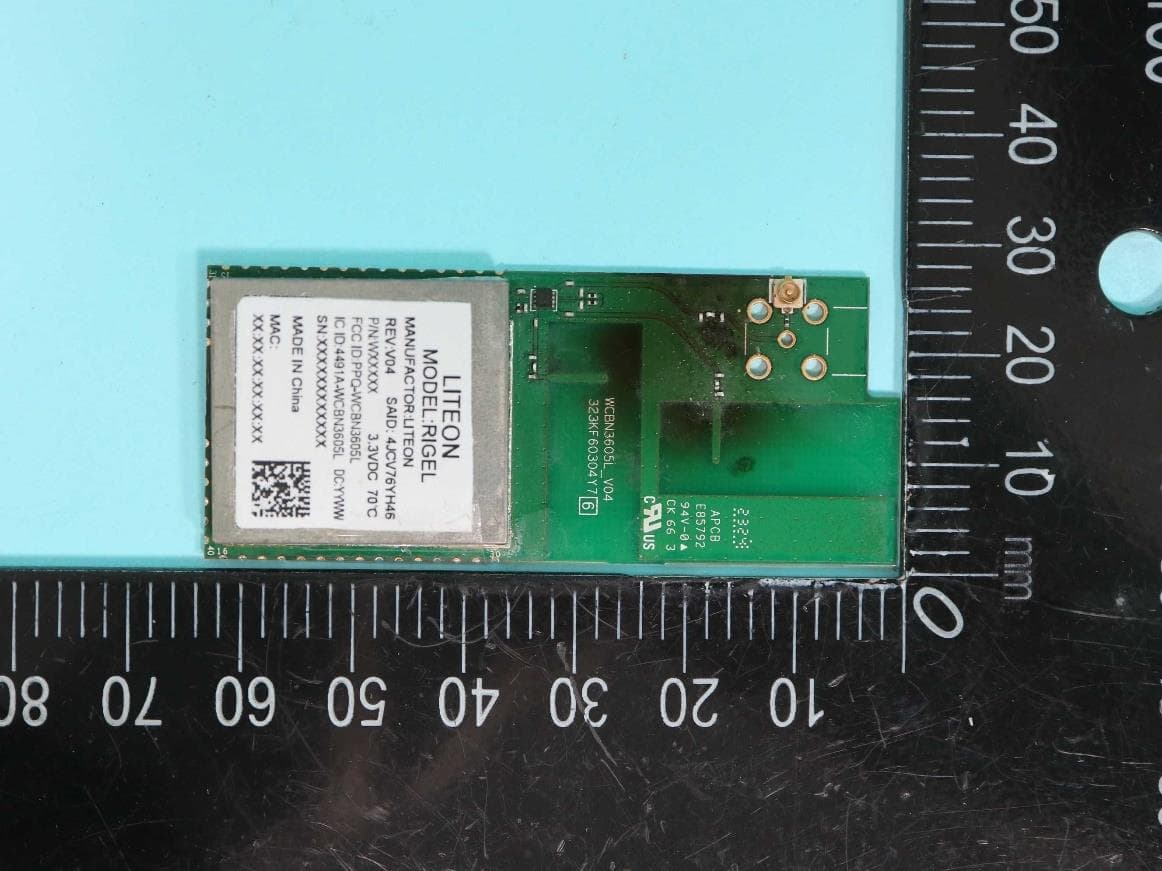
PPQ-WCBN3605L
Aug 30, 2023802.11b/g/n 1Tx1R + BT5.0 IOT Combo Module
Equipment Class
DTS - Digital Transmission System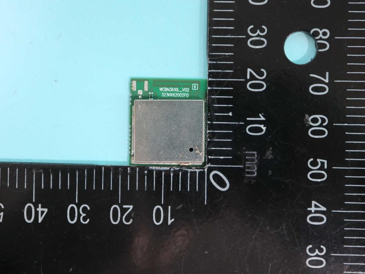
PPQ-WCBN3610L
Jul 24, 2023802.11 b/g/n, 1T1R 2.4G Wireless IoT Module
Equipment Class
DTS - Digital Transmission System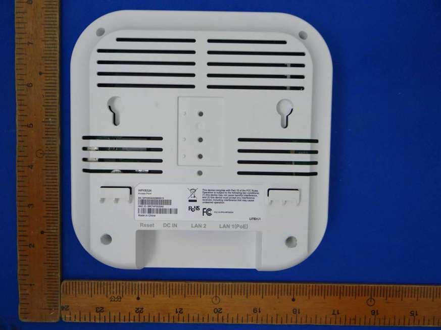
PPQ-WPX8324
Jan 30, 2023Access Point
Equipment Class
DTS - Digital Transmission System
PPQ-WM6321
Dec 16, 2021WM6321
Equipment Class
NII - Unlicensed National Information Infrastructure TX