PWO0725G NR Industrial Signal Booster
Wilson Electronics, LLCApplication Details
- Equipment Class
- B2I - Part 20 Industrial Booster (CMRS)
- Date of Grant
- Aug 26, 2024
- Application Purpose
- Original Equipment
- Date of Application
- Aug 26, 2024
- Equipment Note
- 5G NR Industrial Signal Booster
- Frequency Range
- 3700.00000000 - 3980.00000000
- Company
- Wilson Electronics, LLC
- Country
- United States
Documents & Files
Document Text
Text extracted from the exhibit documents filed with the FCC. Open a document above to read the original.
Attestation Statements
August 7, 2024 Attestation For Wilson Signal Booster: FCC ID PWO072 FEDERAL COMMUNICATIONS COMMISSION Authorization and Evaluation Division 7435 Oakland Mills Road Columbia, MD 21046 RE: Attestation Statements Part 2.911(d)(7) Filing for FCC ID: PWO072 To Whom It May Concern: Ilesh Patel of Wilson Electronics certifies that, as of the date of filing of the application, we designate ourselves as the U.S. agent for service of process. Designated U.S. Agent: Compliance Testing LLC FRN: 0017528332 Name: Wilson Electronics, LLC Address: 3301 E. Deseret Dr., St. George, UT 84790 Contact Person: Ilesh Patel Tel: 469-998-6986 Email: [email protected] Sincerely, Ilesh Patel Senior Engineering Product Manager
Attestation Statements
Federal Communications Commission Authorization and Evaluation Division 7435 Oakland Mills Road Columbia, MD 21046 USA Date: August 7, 2024 Ref: Attestation Statements Part 2.911(d)(5)(i) Filing FCC ID: PWO072 Wilson Electronics LLC (“the applicant”) certifies that the equipment for which authorization is sought is not “covered” equipment prohibited from receiving an equipment authorization pursuant to section 2.903 of the FCC rules. Sincerely, Ilesh Patel Senior Engineering Product Manager Federal Communications Commission Authorization and Evaluation Division 7435 Oakland Mills Road Columbia, MD 21046 USA Date: 05‐09‐2023 Ref: Attestation Statements Part 2.911(d)(5)(ii) Filing FCC ID: PWO074 Wilson Electronics LLC (“the applicant”) certifies that, as of the date of the filing of the application, the applicant is not identified on the Covered List as an entity producing “covered” equipment. Sincerely, Mikel Parry Compliance Manager
Attestation Statements
August 26, 2024 Warning Label Attestation of Wilson Model 460072 Signal Booster Warning label messages will be also shown online and point-of-sale marketing materials and outside packaging of device. Sincerely, Ilesh Patel Senior Engineering Product Manager
Cover Letter(s)
Agent Authorization Letter August 7, 2024 FEDERAL COMMUNICATIONS COMMISSION Authorization and Evaluation Division 7435 Oakland Mills Road Columbia, MD 21046 Subject: Letter of Agent Authorization To Whom It May Concern: Please be advised that we, Wilson Electronics, hereby authorize Compliance Testing LLC to act on our behalf in all matters relating to application for equipment authorization, FCC ID: PWO072, including the signing of all documents relating to these matters. Any and all acts carried out by Wilson Electronics or Compliance Testing LLC in matters pertaining to processes required in the FCC approval shall have the same legal authority as acts and communications by the undersigned. They are authorized to respond to any future issues or FCC requests regarding this project. Please send any query, acknowledgment or response to this letter directly to Wilson Electronics. Sincerely, Ilesh Patel Senior Engineering Product Manager
Cover Letter(s)
August 21, 2024 Feder al Communications Commission 743 5 Oakland Mills Road Columbia, MD 21046 Subject : Data Confidentiality To Wh om It Ma y Concern: Wilson Electronics, Inc. respectfully requests confidentiality of certain documentation provided with the submission of our model 460072 Signal Booster under FCC ID: PWO072 in accordance with sections 0.457 and 0.459 of the Commission’s regulations. We reques t that the followi ng documents be kep t in long-term confidentiality: 1.Schematic Diagram 2.Parts List – Bill of Materials (BOM) 3.Block Diagram 4.Operational Description We request that the following documents be kept in short-term confidentiality until February 28, 2025: 1. Internal Photos 2.Exterior Images 3.Test Setup Photos 4.User Manual The above material is confidential and contains proprietary trade secrets and technical data which must be kept from competitors. Public access to these items could result in duplication of our circuitry and/or techniques thereby reducing our competitive advantage and causing us severe damage. The public disclosure of these materials provides unjustified benefits to its competitors in the market. Sincerely, Ilesh Patel Senior Engineering Product Manager
ID Label/Location Info
WILSON ELECTRONICS, LLC 3301 E. Deseret Dr, St. George, UT 84790 T. 1 800 204 4104 F. 1 435 673 0899 E. [email protected] www.wilsonelectronics.com
Parts List/Tune Up Info
August 21, 2024 Tuning and Adjustment of Wilson Model 460072 Signal Booster There are no external tuning adjustments. The amplifier is factory set to not exceed maximum gains, 28.6 dBm power level, and downlink dependent region (RSSI) set points as provided in the test results. Sincerely, Ilesh Patel Senior Engineering Product Manager
Parts List/Tune Up Info
Antenna Kitting Options August 7, 2024 August 7, 2024 Subject: Antenna Kitting Re: FCC ID: PWO072 To Whom It May Concern: The antenna kitting options for models 460072 signal boosters were done for 2 Outside Antennas, and 3 Inside Antenna kit options. Fixed Outside Antenna 1. Wide Band Directional With 100' LMR 400 310002-952300 Fixed Indoor Antenna All equivalent or lesser antennas and cables are suitable for use with 460072 signal boosters. Sincerely, Ilesh Patel Sr. Engineering Product Manager 2.Wide Band Directional With 100' LMR 400 311245-952300: 1.Inside Antenna Kits 6010026-952300: Dome w/100' Wilson 400 2.Inside Antenna Kits 311243-952300: Panel w/100' Wilson 400 3.Inside Antenna Kits 311242-952300: Dome w/100' Wilson 400 Antenna Kitting Options August 7, 2024 All Outside Antenna Kits with gains less Coax Loss FCC ID: PWO072 Downlink / Uplink Frequency (MHz) 3450 - 3980 All Inside Antenna Kits with gains less Coax Loss FCC ID: PWO072 Wide Band Directional Antenna With 100' Wilson 400 310002-952300 Antenna Gains (dBi) 7 .0 Coax Loss (dB) 9.6 Final Gain less Loss (dB) -2.6 Ins ide Antenna Kit Panel w/100' Wilson 400 311243-952300 Final Gain less Loss (dB) -2.6 Note: Antenna Gain less Coax Loss as Measured Inside Antenna Kit Dome w/100' Wilson 400 6010026-952300 Final Gain less Loss (dB) -4.2 Note: Antenna Gain less Coax Loss as Measured Wide Band Directional Antenna With 100' Wilson 400 311245-952300 Antenna Gains (dBi) 11.5 Coax Loss (dB) 9.6 Final Gain less Loss (dB) 1.9 Ins ide Antenna Kit Dome w/100' Wilson 400 311242-952300 Fin al Gain less Loss (dB) -4.1 No te: Antenna Gain less Coax Loss as Measured
RF Exposure Info
August 18, 2024 Subject: RF MPE EXPOSURE Re: FCC ID: PWO072 To Whom It May Concern: The MPE calculations for model 460072 signal booster were done for 5GNR n77 band frequency range of 3450 -3980 MHz. One calculation was done; this included an highest gain outside antenna, and an highest gain inside antenna that may be connected to this signal booster. The following formula was used to calculate the EIRP: EIRP= Power Out (Watts)*Duty Cycle Percent*Antenna Gain (non‐log)*Coax loss (non‐log) The power density (mW/cm 2 ) is calculated using the following formula: Calculated Power Density=1000*EIRP (Watts)/(4*π*(Distance from Antenna (cm)^2)) Ilesh Patel Senior Engineering Product Manager Sincerely, Minimum Safe Distance From Antennas Based upon FCC OET Bulletin 65 and other FCC Sources Downlink – 3450 MHz Minimum Safe Distance From Antennas Based upon FCC OET Bulletin 65 and other FCC Sources Uplink – 3450 MHz
Test Report
P2470003_FCC_ Part 20_Rev 1.0 Page 1 of 25 Test Report Prepared for: Wilson Electronics, LLC (weBoost) Model: Enterprise 1398 Description: 5G NR Industrial Signal Booster FCC ID: PWO072 To FCC Part 20 FCC Part 27 Date of Issue: August 13, 2024 On the behalf of the applicant: Wilson Electronics, LLC (weBoost) 3301 E Deseret Drive St. George, UT 84790 Attention of: Ilesh Patel, Senior Engineering Product Manager Ph: (435)673-5021 Email: [email protected] Prepared By Compliance Testing, LLC 1724 S. Nevada Way Mesa, AZ 85204 (480) 926-3100 phone / (480) 926-3598 fax www.compliancetesting.com Project No: p2470003 Greg Corbin Project Test Engineer This report may not be reproduced, except in full, without written permission from Compliance Testing All results contained herein relate only to the sample tested P2470003_FCC_ Part 20_Rev 1.0 Page 2 of 25 Test Report Revision History Revision Date Revised By Reason for Revision 1.0 August 13, 2024 Greg Corbin Original Document P2470003_FCC_ Part 20_Rev 1.0 Page 3 of 25 Table of Contents Description Page Table of Annexes 3 Test Result Summary 4 Standard Test Conditions and Engineering Practices 6 AGC Threshold 8 Out-Of-Band Rejection 9 Input-Versus-Output Signal Comparison 10 Mean Output and Amplifier Gain 11 Out-Of-Band/Block Emission (Dual Carrier) 12 Out-Of-Band/Block Emission (Single Carrier) 14 Conducted Spurious Emissions 16 Radiated Spurious Emissions 21 Measurement Uncertainty 24 Test Equipment Utilized 25 Table of Annexes Description Page Annex A – Out of Band Rejection 9 Annex B – Input vs Output Signal Comparison 10 Annex C - Out of Band/Block Emission (Dual Carrier)_3450 – 3550 MHz 13 Annex D_ Out of Band/Block Emission (Dual Carrier)_3700 - 3980 MHz 13 Annex E - Out of Band/Block Emission (Single Carrier)_3450 – 3550 MHz 15 Annex F - Out of Band/Block Emission (Single Carrier)_3700 - 3980 MHz 15 Annex G – Conducted Spurious Emission_3450 – 3550 MHz 20 Annex H – Conducted Spurious Emission_3700 – 3980 MHz 20 Annex I – Radiated Spurious Emission_3450 – 3550 MHz 23 Annex J – Radiated Spurious Emission_3700 – 3980 MHz 23 P2470003_FCC_ Part 20_Rev 1.0 Page 4 of 25 Test Result Summary Receipt of Sample: July 24, 21024 Test Date Range: July 25, 2024 – August 12, 2024 Specification Test Name Pass, Fail, N/A Comments KDB 935210 D05 AGC Threshold Pass KDB 935210 D05 Out-of-Band Rejection Pass KDB 935210 D05 Input-Versus-Output Signal Comparison Pass 2.1046 27.50(j) 27.50(k) KDB 935210 D05 Mean Output Power and Amplifier gain Pass 2.1049 27.53(l)(1) 27.53(n)(1) KDB 935210 D05 Out-Of-Band/Block Emissions Conducted Pass 2.1051 27.53(l)(1) 27.53(n)(1) KDB 935210 D05 Spurious Emissions Conducted Pass 2.1053 27.53(l)(1) 27.53(n)(1) KDB 935210 D05 Spurious Emissions Radiated Pass KDB 935210 D05 Frequency Stability N/A Does not have Frequency translation Statements of conformity are reported as: • Pass - the measured value is below the acceptance limit, acceptance limit = test limit. • Fail - the measured value is above the acceptance limit, acceptance limit = test limit. P2470003_FCC_ Part 20_Rev 1.0 Page 5 of 25 ANAB Compliance Testing, LLC, has been accredited in accordance with the recognized International Standard ISO/IEC 17025:2017. This accreditation demonstrates technical competence for a defined scope and the operation of a laboratory quality management system (refer to the joint ISO-ILAC-IAF Communiqué dated January 2009). The tests results contained within this test report all fall within our scope of accreditation, unless noted below. Please refer to http://www.compliancetesting.com/labscope.html for current scope of accreditation. FCC Site Reg. #349717 IC Site Reg. #2044A-2 P2470003_FCC_ Part 20_Rev 1.0 Page 6 of 25 Test and Measurement Data All tests and measurement data shown were performed in accordance with FCC Rules and Regulations, KDB 935210 D05 Industrial Booster Basic Measurements v01r04, ANSI C63-26:2015 and FCC Part 2, Part 20.21, Part 27 where appropriate. Standard Test Conditions and Engineering Practices Except as noted herein, the following conditions and procedures were observed during the testing. In accordance with ANSI/TIA 603C, and unless otherwise indicated in the specific measurement results, the ambient temperature of the actual EUT was maintained within the range of 10° to 40°C (50° to 104°F) unless the particular equipment requirements specify testing over a different temperature range. Also, unless otherwise indicated, the humidity levels were in the range of 10% to 90% relative humidity. Environmental Conditions Temp (ºC) Humidity (%) Pressure (mbar) 25.3 – 30.8 38.7 – 62.9 968 - 970.58 Measurement results, unless otherwise noted, are worst-case measurements. EUT Description Model: Enterprise 1398 460072 (wall mount) S/N: 102142277 HVIN: 460072, PMN: 460072 Model: Enterprise 1398 461072 (rack mount) S/N: 102142415 HVIN: 461072, PMN: 461072 Description: 5G NR Industrial Signal Booster Highest Clock Frequency: 122.88 MHz Additional Information: The Equipment Under Test (EUT) is a bi -directional industrial signal booster. The test data contained in this report pertains only to the emissions due to the 5G-NR operation. The test data contained in this report covers both uplink and downlink operation for the booster device. This EUT is capable of transmitting boosted 5G-NR TDD signals with the internal bi -directional amplifier. The EUT does not generate its own RF. The EUT supports any combination of 5G-NR n77 band bandwidths, number of carriers, and modulations. The EUT supports the frequency bands, modulation and bandwidths listed in Table 1. The EUT will transmit all signals within the 5G-NR n77 band that are received. The EUT has 2 donor ports and 2 server ports all with an impedance of 50 ohms. The ports are referred to as Main and Aux ports, Main Uplink (UL) and Main Downlink (DL), Aux UL and Aux DL. The server ports are tested by inputting uplink signal on server ports as input port and measured outpu…
Text truncated - open the document above for the full version.
Test Report
P2470003_Annex A _ Rev 1.0 Page 1 of 5 Annex A Out of Band Rejection P2470003_Annex A _ Rev 1.0 Page 2 of 5 Out of Band Rejection_ aux port_DL_3.45 - 3.55 GHz Out of Band Rejection_ aux port_DL_3.70 - 3.98 GHz P2470003_Annex A _ Rev 1.0 Page 3 of 5 Out of Band Rejection_ aux port_UL_3.45 - 3.55 GHz Out of Band Rejection_ aux port_UL_3.70 - 3.98 GHz P2470003_Annex A _ Rev 1.0 Page 4 of 5 Out of Band Rejection_ main port_DL_3.45 - 3.55 GHz Out of Band Rejection_ main port_DL_3.70 - 3.98 GHz P2470003_Annex A _ Rev 1.0 Page 5 of 5 Out of Band Rejection_ main port_UL_3.45 - 3.55 GHz Out of Band Rejection_ main port_UL_3.70 - 3.98 GHz
Test Report
P2470003_Annex C _ Rev 1.0 Page 1 of 33 Annex C Out of Band/Block Emission (Dual Carrier) 3450 – 3550 MHz P2470003_Annex C _ Rev 1.0 Page 2 of 33 Dual Carrier OOBE_high side_3550 - 3553 MHz_ aux DL_20 MHz BW_RBW =1 MHz Dual Carrier OOBE_high side_3550 - 3553 MHz_ aux DL_20 MHz BW_RBW =1 MHz_Pin + 3 dB P2470003_Annex C _ Rev 1.0 Page 3 of 33 Dual Carrier OOBE_high side_3550 - 3553 MHz_ aux DL_20 MHz BW_RBW =200 kHz Dual Carrier OOBE_high side_3550 - 3553 MHz_ aux DL_20 MHz BW_RBW =200 kHz_Pin + 3 dB P2470003_Annex C _ Rev 1.0 Page 4 of 33 Dual Carrier OOBE_high side_3550 - 3553 MHz_ aux DL_40 MHz BW_RBW =1 MHz Dual Carrier OOBE_high side_3550 - 3553 MHz_ aux DL_40 MHz BW_RBW =1 MHz_Pin + 3 dB P2470003_Annex C _ Rev 1.0 Page 5 of 33 Dual Carrier OOBE_high side_3550 - 3553 MHz_ aux DL_40 MHz BW_RBW =200 kHz Dual Carrier OOBE_high side_3550 - 3553 MHz_ aux DL_40 MHz BW_RBW =200 kHz_Pin + 3 dB P2470003_Annex C _ Rev 1.0 Page 6 of 33 Dual Carrier OOBE_high side_3550 - 3553 MHz_ aux UL_20 MHz BW_RBW =1 MHz Dual Carrier OOBE_high side_3550 - 3553 MHz_ aux UL_20 MHz BW_RBW =1 MHz_Pin + 3 dB P2470003_Annex C _ Rev 1.0 Page 7 of 33 Dual Carrier OOBE_high side_3550 - 3553 MHz_ aux UL_20 MHz BW_RBW =200 kHz Dual Carrier OOBE_high side_3550 - 3553 MHz_ aux UL_20 MHz BW_RBW =200 kHz_Pin + 3 dB P2470003_Annex C _ Rev 1.0 Page 8 of 33 Dual Carrier OOBE_high side_3550 - 3553 MHz_ aux UL_40 MHz BW_RBW = 200 kHz Dual Carrier OOBE_high side_3550 - 3553 MHz_ aux UL_40 MHz BW_RBW = 200 kHz_Pin + 3 dB P2470003_Annex C _ Rev 1.0 Page 9 of 33 Dual Carrier OOBE_high side_3550 - 3553 MHz_ aux UL_40 MHz BW_RBW =1 MHz Dual Carrier OOBE_high side_3550 - 3553 MHz_ aux UL_40 MHz BW_RBW =1 MHz_Pin + 3 dB P2470003_Annex C _ Rev 1.0 Page 10 of 33 Dual Carrier OOBE_high side_3550 - 3553 MHz_ main DL_20 MHz BW_RBW =1 MHz Dual Carrier OOBE_high side_3550 - 3553 MHz_ main DL_20 MHz BW_RBW =1 MHz_Pin + 3 dB P2470003_Annex C _ Rev 1.0 Page 11 of 33 Dual Carrier OOBE_high side_3550 - 3553 MHz_ main DL_20 MHz BW_RBW =200 kHz Dual Carrier OOBE_high side_3550 - 3553 MHz_ main DL_20 MHz BW_RBW =200 kHz_Pin + 3 dB P2470003_Annex C _ Rev 1.0 Page 12 of 33 Dual Carrier OOBE_high side_3550 - 3553 MHz_ main DL_40 MHz BW_RBW =1 MHz Dual Carrier OOBE_high side_3550 - 3553 MHz_ main DL_40 MHz BW_RBW =1 MHz_Pin + 3 dB P2470003_Annex C _ Rev 1.0 Page 13 of 33 Dual Carrier OOBE_high side_3550 - 3553 MHz_ main DL_40 MHz BW_RBW =200 kHz Dual Carrier OOBE_high side_3550 - 3553 MHz_ main DL_40 MHz BW_RBW =200 kHz_Pin + 3 dB P2470003_Annex C _ Rev 1.0 Page 14 of 33 Dual Carrier OOBE_high side_3550 - 3553 MHz_ main UL_20 MHz BW_RBW =1 MHz Dual Carrier OOBE_high side_3550 - 3553 MHz_ main UL_20 MHz BW_RBW =1 MHz_Pin + 3 dB P2470003_Annex C _ Rev 1.0 Page 15 of 33 Dual Carrier OOBE_high side_3550 - 3553 MHz_ main UL_20 MHz BW_RBW =200 kHz Dual Carrier OOBE_high side_3550 - 3553 MHz_ main UL_20 MHz BW_RBW =200 kHz_Pin + 3 dB P2470003_Annex C _ Rev 1.0 Page 16 of 33 Dual Carrier OOBE_high side_3550 - 3553 MHz_ main UL_40 MHz BW_RBW =1 MHz Dual Carrier OOBE_high side_3550 - 3553 MHz_ main UL_40 MHz BW_RBW =1 MHz_Pin + 3 dB P2470003_Annex C _ Rev 1.0 Page 17 of 33 Dual Carrier OOBE_high side_3550 - 3553 MHz_ main UL_40 MHz BW_RBW =200 kHz Dual Carrier OOBE_high side_3550 - 3553 MHz_ main UL_40 MHz BW_RBW =200 kHz_Pin + 3 dB P2470003_Annex C _ Rev 1.0 Page 18 of 33 Dual Carrier OOBE_low side_3447 - 3750 MHz_ aux DL_20 MHz BW_RBW = 1 MHz Dual Carrier OOBE_low side_3447 - 3750 MHz_ aux DL_20 MHz BW_RBW = 1 MHz_Pin + 3 dB P2470003_Annex C _ Rev 1.0 Page 19 of 33 Dual Carrier OOBE_low side_3447 - 3750 MHz_ aux DL_20 MHz BW_RBW = 200 kHz Dual Carrier OOBE_low side_3447 - 3750 MHz_ aux DL_20 MHz BW_RBW = 200 kHz_Pin + 3 dB P2470003_Annex C _ Rev 1.0 Page 20 of 33 Dual Carrier OOBE_low side_3447 - 3750 MHz_ aux DL_40 MHz BW_RBW = 1 MHz Dual Carrier OOBE_low side_3447 - 3750 MHz_ aux DL_40 MHz BW_RBW = 1 MHz_Pin + 3 dB P2470003_Annex C _ Rev 1.0 Page 21 of 33 Dual Carrier OOBE_low side_3447 - 3750 MHz_ aux DL_40 MHz BW_RBW = 200 kHz Dual Carrier OOBE_low side_3447 - 3750 MHz_ aux DL_40 MHz BW_RBW = 200 kHz_Pin + 3 dB P2470003_Annex C _ Rev 1.0 Page 22 of 33 Dual Carrier OOBE_low side_3447 - 3750 MHz_ aux UL_20 MHz BW_RBW = 1 MHz Dual Carrier OOBE_low side_3447 - 3750 MHz_ aux UL_20 MHz BW_RBW = 1 MHz_Pin + 3 dB P2470003_Annex C _ Rev 1.0 Page 23 of 33 Dual Carrier OOBE_low side_3447 - 3750 MHz_ aux UL_20 MHz BW_RBW = 200 kHz Dual Carrier OOBE_low side_3447 - 3750 MHz_ aux UL_20 MHz BW_RBW =200 kHz_Pin + 3 dB P2470003_Annex C _ Rev 1.0 Page 24 of 33 Dual Carrier OOBE_low side_3447 - 3750 MHz_ aux UL_40 MHz BW_RBW = 1 MHz Dual Carrier OOBE_low side_3447 - 3750 MHz_ aux UL_40 MHz BW_RBW = 1 MHz_Pin + 3 dB P2470003_Annex C _ Rev 1.0 Page 25 of 33 Dual Carrier OOBE_low side_3447 - 3750 MHz_ aux UL_40 MHz BW_RBW = 200 kHz Dual Carrier OOBE_low side_3447 - 3750 MHz_ aux UL_40 MHz BW_RBW = 200 kHz_Pin + 3 dB P2470003_Annex C _ Rev 1.0 Page 26 of 33 Dual Carrier OOBE_low side_3447 - 3750 MHz_ main DL_20 MHz BW_RBW = 1 MHz Dual Carrier OOBE_low side_3447 - 3750 MHz_ main DL_20 MHz BW_RBW = 1 MHz_pin + 3 dB P2470003_Annex C _ Rev 1.0 Page 27 of 33 Dual Carrier OOBE_low side_3447 - 3750 MHz_ main DL_20 MHz BW_RBW = 200 kHz Dual Carrier OOBE_low side_3447 - 3750 MHz_ main DL_20 MHz BW_RBW = 200 kHz_pin + 3 dB P2470003_Annex C _ Rev 1.0 Page 28 of 33 Dual Carrier OOBE_low side_3447 - 3750 MHz_ main DL_40 MHz BW_RBW = 1 MHz Dual Carrier OOBE_low side_3447 - 3750 MHz_ main DL_40 MHz BW_RBW = 1 MHz_Pin + 3 dB P2470003_Annex C _ Rev 1.0 Page 29 of 33 Dual Carrier OOBE_low side_3447 - 3750 MHz_ main DL_40 MHz BW_RBW = 200 kHz Dual Carrier OOBE_low side_3447 - 3750 MHz_ main DL_40 MHz BW_RBW = 200 kHz_Pin + 3 dB P2470003_Annex C _ Rev 1.0 Page 30 of 33 Dual Carrier OOBE_low side_3447 - 3750 MHz_ main UL_20 MHz BW_RBW =1 MHz Dual Carrier OOBE_low side_3447 - 3750 MHz_ main UL_20 MHz BW_RBW =1 MHz_Pin + 3 dB P2470003_Annex C _ Rev 1.0 Page 31 of 33 Dual Carrier OOBE_low side_3447 - 3750…
Text truncated - open the document above for the full version.
Test Report
P2470003_Annex D _ Rev 1.0 Page 1 of 33 Annex D Out of Band/Block Emission (Dual Carrier) 3700 - 3980 MHz P2470003_Annex D _ Rev 1.0 Page 2 of 33 Dual Carrier OOBE_high side_3980 - 3983 MHz_aux DL_20 MHz BW_RBW = 1 MHz Dual Carrier OOBE_high side_3980 - 3983 MHz_aux DL_20 MHz BW_RBW = 1 MHz_Pin + 3 dB P2470003_Annex D _ Rev 1.0 Page 3 of 33 Dual Carrier OOBE_high side_3980 - 3983 MHz_aux DL_20 MHz BW_RBW = 200 kHz Dual Carrier OOBE_high side_3980 - 3983 MHz_aux DL_20 MHz BW_RBW = 200 kHz_Pin + 3 dB P2470003_Annex D _ Rev 1.0 Page 4 of 33 Dual Carrier OOBE_high side_3980 - 3983 MHz_aux UL_20 MHz BW_RBW = 1 MHz Dual Carrier OOBE_high side_3980 - 3983 MHz_aux UL_20 MHz BW_RBW = 1 MHz_Pin + 3 dB P2470003_Annex D _ Rev 1.0 Page 5 of 33 Dual Carrier OOBE_high side_3980 - 3983 MHz_aux UL_20 MHz BW_RBW = 200 kHz Dual Carrier OOBE_high side_3980 - 3983 MHz_aux UL_20 MHz BW_RBW = 200 kHz_Pin + 3 dB P2470003_Annex D _ Rev 1.0 Page 6 of 33 Dual Carrier OOBE_high side_3980 - 3983 MHz_main DL_20 MHz BW_RBW = 1 MHz Dual Carrier OOBE_high side_3980 - 3983 MHz_main DL_20 MHz BW_RBW = 1 MHz_Pin + 3 dB P2470003_Annex D _ Rev 1.0 Page 7 of 33 Dual Carrier OOBE_high side_3980 - 3983 MHz_main DL_20 MHz BW_RBW = 200 kHz Dual Carrier OOBE_high side_3980 - 3983 MHz_main DL_20 MHz BW_RBW = 200 kHz_Pin + 3 dB P2470003_Annex D _ Rev 1.0 Page 8 of 33 Dual Carrier OOBE_high side_3980 - 3983 MHz_main UL_20 MHz BW_RBW = 1 MHz Dual Carrier OOBE_high side_3980 - 3983 MHz_main UL_20 MHz BW_RBW = 1 MHz_Pin + 3 dB P2470003_Annex D _ Rev 1.0 Page 9 of 33 Dual Carrier OOBE_high side_3980 - 3983 MHz_main UL_20 MHz BW_RBW = 200 kHz Dual Carrier OOBE_high side_3980 - 3983 MHz_main UL_20 MHz BW_RBW = 200 kHz_Pin + 3 dB P2470003_Annex D _ Rev 1.0 Page 10 of 33 Dual Carrier OOBE_high side_3980 - 3983 MHz_ aux DL_100 MHz BW_RBW = 1 MHz Dual Carrier OOBE_high side_3980 - 3983 MHz_ aux DL_100 MHz BW_RBW = 1 MHz_Pin + 3 dB P2470003_Annex D _ Rev 1.0 Page 11 of 33 Dual Carrier OOBE_high side_3980 - 3983 MHz_ aux DL_100 MHz BW_RBW = 200 kHz Dual Carrier OOBE_high side_3980 - 3983 MHz_ aux DL_100 MHz BW_RBW = 200 kHz_Pin + 3 dB P2470003_Annex D _ Rev 1.0 Page 12 of 33 Dual Carrier OOBE_high side_3980 - 3983 MHz_ aux UL_100 MHz BW_RBW = 1 MHz Dual Carrier OOBE_high side_3980 - 3983 MHz_ aux UL_100 MHz BW_RBW = 1 MHz_Pin + 3 dB P2470003_Annex D _ Rev 1.0 Page 13 of 33 Dual Carrier OOBE_high side_3980 - 3983 MHz_ aux UL_100 MHz BW_RBW = 200 kHz Dual Carrier OOBE_high side_3980 - 3983 MHz_ aux UL_100 MHz BW_RBW = 200 kHz_Pin + 3 dB P2470003_Annex D _ Rev 1.0 Page 14 of 33 Dual Carrier OOBE_high side_3980 - 3983 MHz_ main DL_100 MHz BW_RBW = 1 MHz Dual Carrier OOBE_high side_3980 - 3983 MHz_ main DL_100 MHz BW_RBW = 1 MHz_Pin + 3 dB P2470003_Annex D _ Rev 1.0 Page 15 of 33 Dual Carrier OOBE_high side_3980 - 3983 MHz_ main DL_100 MHz BW_RBW = 200 kHz Dual Carrier OOBE_high side_3980 - 3983 MHz_ main DL_100 MHz BW_RBW = 200 kHz_Pin + 3 dB P2470003_Annex D _ Rev 1.0 Page 16 of 33 Dual Carrier OOBE_high side_3980 - 3983 MHz_ main UL_100 MHz BW_RBW = 1 MHz Dual Carrier OOBE_high side_3980 - 3983 MHz_ main UL_100 MHz BW_RBW = 1 MHz_Pin + 3 dB P2470003_Annex D _ Rev 1.0 Page 17 of 33 Dual Carrier OOBE_high side_3980 - 3983 MHz_ main UL_100 MHz BW_RBW = 200 kHz Dual Carrier OOBE_high side_3980 - 3983 MHz_ main UL_100 MHz BW_RBW =200 kHz_Pin + 3 dB P2470003_Annex D _ Rev 1.0 Page 18 of 33 Dual Carrier OOBE_low side_3697 - 3700 MHz_ aux DL_100 MHz BW_RBW = 1 MHz Dual Carrier OOBE_low side_3697 - 3700 MHz_ aux DL_100 MHz BW_RBW = 1 MHz_Pin + 3 dB P2470003_Annex D _ Rev 1.0 Page 19 of 33 Dual Carrier OOBE_low side_3697 - 3700 MHz_ aux DL_100 MHz BW_RBW = 200 kHz Dual Carrier OOBE_low side_3697 - 3700 MHz_ aux DL_100 MHz BW_RBW = 200 kHz_Pin + 3 dB P2470003_Annex D _ Rev 1.0 Page 20 of 33 Dual Carrier OOBE_low side_3697 - 3700 MHz_ aux DL_20 MHz BW_RBW = 1 MHz Dual Carrier OOBE_low side_3697 - 3700 MHz_ aux DL_20 MHz BW_RBW = 1 MHz_Pin + 3 dB P2470003_Annex D _ Rev 1.0 Page 21 of 33 Dual Carrier OOBE_low side_3697 - 3700 MHz_ aux DL_20 MHz BW_RBW = 200 kHz Dual Carrier OOBE_low side_3697 - 3700 MHz_ aux DL_20 MHz BW_RBW = 200 kHz_Pin + 3 dB P2470003_Annex D _ Rev 1.0 Page 22 of 33 Dual Carrier OOBE_low side_3697 - 3700 MHz_ aux UL_100 MHz BW_RBW = 1 MHz Dual Carrier OOBE_low side_3697 - 3700 MHz_ aux UL_100 MHz BW_RBW = 1 MHz_Pin + 3 dB P2470003_Annex D _ Rev 1.0 Page 23 of 33 Dual Carrier OOBE_low side_3697 - 3700 MHz_ aux UL_100 MHz BW_RBW = 200 kHz Dual Carrier OOBE_low side_3697 - 3700 MHz_ aux UL_100 MHz BW_RBW = 200 kHz_Pin + 3 dB P2470003_Annex D _ Rev 1.0 Page 24 of 33 Dual Carrier OOBE_low side_3697 - 3700 MHz_ aux UL_20 MHz BW_RBW = 1 MHz Dual Carrier OOBE_low side_3697 - 3700 MHz_ aux UL_20 MHz BW_RBW = 1 MHz_Pin + 3 dB P2470003_Annex D _ Rev 1.0 Page 25 of 33 Dual Carrier OOBE_low side_3697 - 3700 MHz_ aux UL_20 MHz BW_RBW = 200 kHz Dual Carrier OOBE_low side_3697 - 3700 MHz_ aux UL_20 MHz BW_RBW = 200 kHz_Pin + 3 dB P2470003_Annex D _ Rev 1.0 Page 26 of 33 Dual Carrier OOBE_low side_3697 - 3700 MHz_ main DL_100 MHz BW_RBW = 1 MHz Dual Carrier OOBE_low side_3697 - 3700 MHz_ main DL_100 MHz BW_RBW = 1 MHz_Pin + 3 dB P2470003_Annex D _ Rev 1.0 Page 27 of 33 Dual Carrier OOBE_low side_3697 - 3700 MHz_ main DL_100 MHz BW_RBW = 200 kHz Dual Carrier OOBE_low side_3697 - 3700 MHz_ main DL_100 MHz BW_RBW = 200 kHz_Pin + 3 dB P2470003_Annex D _ Rev 1.0 Page 28 of 33 Dual Carrier OOBE_low side_3697 - 3700 MHz_ main DL_20 MHz BW_RBW = 1 MHz Dual Carrier OOBE_low side_3697 - 3700 MHz_ main DL_20 MHz BW_RBW = 1 MHz_Pin + 3 dB P2470003_Annex D _ Rev 1.0 Page 29 of 33 Dual Carrier OOBE_low side_3697 - 3700 MHz_ main DL_20 MHz BW_RBW = 200 kHz Dual Carrier OOBE_low side_3697 - 3700 MHz_ main DL_20 MHz BW_RBW = 200 kHz_Pin + 3 dB P2470003_Annex D _ Rev 1.0 Page 30 of 33 Dual Carrier OOBE_low side_3697 - 3700 MHz_ main UL_100 MHz BW_RBW = 1 MHz Dual Carrier OOBE_low side_3697 - 3700 MHz_ main UL_100 MHz BW_RBW = 1 MHz_Pin + 3 dB P2470003_Annex D _ Rev 1.0 Page 3…
Text truncated - open the document above for the full version.
Test Report
P2470003_Annex E _ Rev 1.0 Page 1 of 33 Annex E Out of Band/Block Emission (Single Carrier) 3450 – 3550 MHz P2470003_Annex E _ Rev 1.0 Page 2 of 33 Single Carrier OOBE_high side_3450 - 3453 MHz_ aux DL_20 MHz BW_RBW =1 MHz Single Carrier OOBE_high side_3450 - 3453 MHz_ aux DL_20 MHz BW_RBW =1 MHz_Pin + 3 dB P2470003_Annex E _ Rev 1.0 Page 3 of 33 Single Carrier OOBE_high side_3450 - 3453 MHz_ aux DL_20 MHz BW_RBW =200 kHz Single Carrier OOBE_high side_3450 - 3453 MHz_ aux DL_20 MHz BW_RBW =200 kHz_Pin + 3 dB P2470003_Annex E _ Rev 1.0 Page 4 of 33 Single Carrier OOBE_high side_3450 - 3453 MHz_ aux DL_40 MHz BW_RBW =1 MHz Single Carrier OOBE_high side_3450 - 3453 MHz_ aux DL_40 MHz BW_RBW =1 MHz_Pin + 3 dB P2470003_Annex E _ Rev 1.0 Page 5 of 33 Single Carrier OOBE_high side_3450 - 3453 MHz_ aux DL_40 MHz BW_RBW =200 kHz Single Carrier OOBE_high side_3450 - 3453 MHz_ aux DL_40 MHz BW_RBW =200 kHz_Pin + 3 dB P2470003_Annex E _ Rev 1.0 Page 6 of 33 Single Carrier OOBE_high side_3450 - 3453 MHz_ aux UL_20 MHz BW_RBW =1 MHz Single Carrier OOBE_high side_3450 - 3453 MHz_ aux UL_20 MHz BW_RBW =1 MHz_Pin + 3 dB P2470003_Annex E _ Rev 1.0 Page 7 of 33 Single Carrier OOBE_high side_3450 - 3453 MHz_ aux UL_20 MHz BW_RBW =200 kHz Single Carrier OOBE_high side_3450 - 3453 MHz_ aux UL_20 MHz BW_RBW =200 kHz_Pin + 3 dB P2470003_Annex E _ Rev 1.0 Page 8 of 33 Single Carrier OOBE_high side_3450 - 3453 MHz_ aux UL_40 MHz BW_RBW =1 MHz Single Carrier OOBE_high side_3450 - 3453 MHz_ aux UL_40 MHz BW_RBW =1 MHz_Pin + 3 dB P2470003_Annex E _ Rev 1.0 Page 9 of 33 Single Carrier OOBE_high side_3450 - 3453 MHz_ aux UL_40 MHz BW_RBW =200 kHz Single Carrier OOBE_high side_3450 - 3453 MHz_ aux UL_40 MHz BW_RBW =200 kHz_Pin + 3 dB P2470003_Annex E _ Rev 1.0 Page 10 of 33 Single Carrier OOBE_high side_3450 - 3453 MHz_ main DL_20 MHz BW_RBW =1 MHz Single Carrier OOBE_high side_3450 - 3453 MHz_ main DL_20 MHz BW_RBW =1 MHz_Pin + 3 dB P2470003_Annex E _ Rev 1.0 Page 11 of 33 Single Carrier OOBE_high side_3450 - 3453 MHz_ main DL_20 MHz BW_RBW =200 kHz Single Carrier OOBE_high side_3450 - 3453 MHz_ main DL_20 MHz BW_RBW =200 kHz_Pin + 3 dB P2470003_Annex E _ Rev 1.0 Page 12 of 33 Single Carrier OOBE_high side_3450 - 3453 MHz_ main DL_40 MHz BW_RBW =1 MHz Single Carrier OOBE_high side_3450 - 3453 MHz_ main DL_40 MHz BW_RBW =1 MHz_Pin + 3 dB P2470003_Annex E _ Rev 1.0 Page 13 of 33 Single Carrier OOBE_high side_3450 - 3453 MHz_ main DL_40 MHz BW_RBW =200 kHz Single Carrier OOBE_high side_3450 - 3453 MHz_ main DL_40 MHz BW_RBW =200 kHz_Pin + 3 dB P2470003_Annex E _ Rev 1.0 Page 14 of 33 Single Carrier OOBE_high side_3450 - 3453 MHz_ main UL_20 MHz BW_RBW =1 MHz Single Carrier OOBE_high side_3450 - 3453 MHz_ main UL_20 MHz BW_RBW =1 MHz_Pin + 3 dB P2470003_Annex E _ Rev 1.0 Page 15 of 33 Single Carrier OOBE_high side_3450 - 3453 MHz_ main UL_20 MHz BW_RBW =200 kHz Single Carrier OOBE_high side_3450 - 3453 MHz_ main UL_20 MHz BW_RBW =200 kHz_Pin + 3 dB P2470003_Annex E _ Rev 1.0 Page 16 of 33 Single Carrier OOBE_high side_3450 - 3453 MHz_ main UL_40 MHz BW_RBW =1 MHz Single Carrier OOBE_high side_3450 - 3453 MHz_ main UL_40 MHz BW_RBW =1 MHz_Pin + 3 dB P2470003_Annex E _ Rev 1.0 Page 17 of 33 Single Carrier OOBE_high side_3450 - 3453 MHz_ main UL_40 MHz BW_RBW =200 kHz Single Carrier OOBE_high side_3450 - 3453 MHz_ main UL_40 MHz BW_RBW =200 kHz_Pin + 3 dB P2470003_Annex E _ Rev 1.0 Page 18 of 33 Single Carrier OOBE_low side_3447 - 3450 MHz_ aux DL_20 MHz BW_RBW =1 MHz Single Carrier OOBE_low side_3447 - 3450 MHz_ aux DL_20 MHz BW_RBW =1 MHz_Pin + 3 dB P2470003_Annex E _ Rev 1.0 Page 19 of 33 Single Carrier OOBE_low side_3447 - 3450 MHz_ aux DL_20 MHz BW_RBW =200 kHz Single Carrier OOBE_low side_3447 - 3450 MHz_ aux DL_20 MHz BW_RBW =200 kHz_Pin + 3 dB P2470003_Annex E _ Rev 1.0 Page 20 of 33 Single Carrier OOBE_low side_3447 - 3450 MHz_ aux DL_40 MHz BW_RBW =1 MHz Single Carrier OOBE_low side_3447 - 3450 MHz_ aux DL_40 MHz BW_RBW =1 MHz_Pin + 3 dB P2470003_Annex E _ Rev 1.0 Page 21 of 33 Single Carrier OOBE_low side_3447 - 3450 MHz_ aux DL_40 MHz BW_RBW =200 kHz Single Carrier OOBE_low side_3447 - 3450 MHz_ aux DL_40 MHz BW_RBW =200 kHz_Pin + 3 dB P2470003_Annex E _ Rev 1.0 Page 22 of 33 Single Ca…
Text truncated - open the document above for the full version.
Contact Information
Applicant
Ilesh Patel(Senior RF Design Engineer)
Technical Contact
Wilson Electronics LLCIlesh Pate;
[email protected]4699986986
3301 E. Deseret Dr. · St. George, Utah · United States
Test Firm
Compliance Testing, LLCMichael Schafer
[email protected]480-926-3100
Technical Specifications
| # | Rule Parts | Frequency Range | Power Output | Emission | Tolerance |
|---|---|---|---|---|---|
| 4 | 27 | 3.70 GHz - 3.98 GHz | 724.00 mW | W7D | Amp |
Other Applications from Wilson Electronics, LLC
PWO086
Mar 09, 2026Single Band Bi-Directional Amplifier
Equipment Class
B2W - Part 20 Wideband Consumer Booster (CMRS)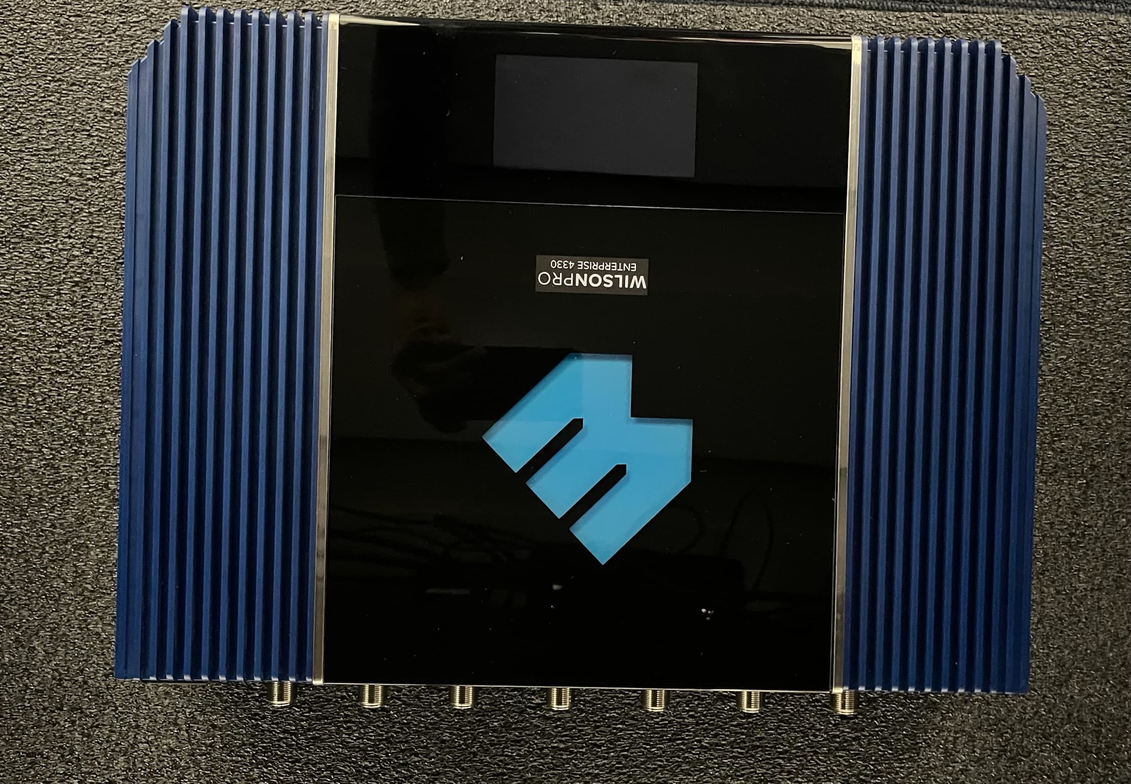
PWO075
Jan 10, 2024Quint Band Signal Booster
Equipment Class
B2W - Part 20 Wideband Consumer Booster (CMRS)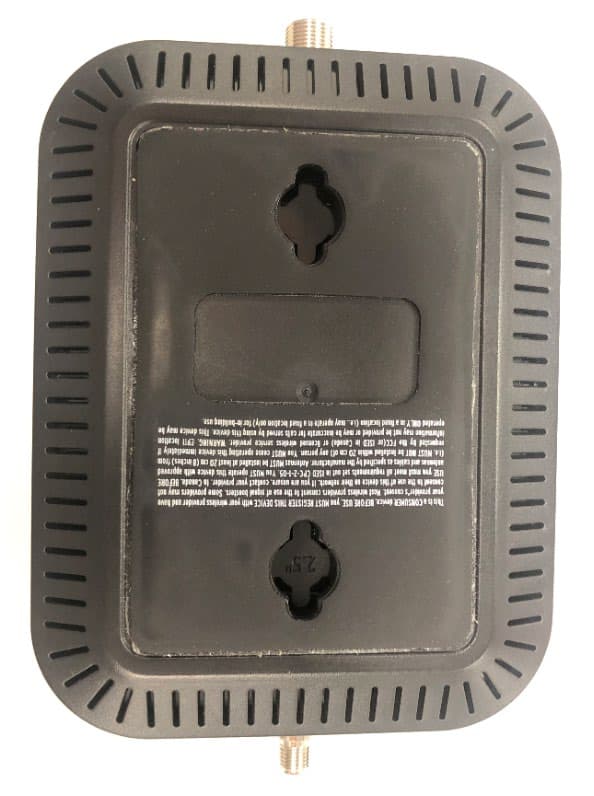
PWO460065
Nov 04, 2020Dual Band Signal Booster
Equipment Class
B2W - Part 20 Wideband Consumer Booster (CMRS)
PWO460061
Sep 22, 2020Quint Band Signal Booster
Equipment Class
B2W - Part 20 Wideband Consumer Booster (CMRS)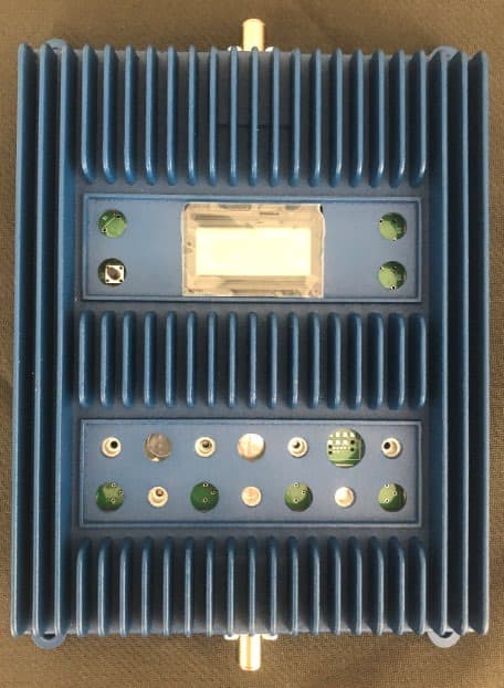
PWO460062
Aug 13, 2020Quint Band Signal Booster
Equipment Class
B2W - Part 20 Wideband Consumer Booster (CMRS)